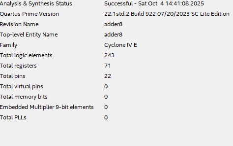
This log presents the first attempt at implementing a full computation chain based on the Residue Number System (RNS) on an FPGA—specifically, a Cyclone IV. Division is systematically avoided in favor of additions, bit shifts, and lookup tables. The complete pipeline, from conversion to reconstruction, is justified step by step. The code is available on my github : https://github.com/Bertrand-selvasystems/RNS-on-FPGA/.
Hardware and development environment
The hardware target is a Cyclone IV FPGA (EP4CE family). Physical programming will be performed later, as soon as the programmer arrives (ordered from Aliexpress, this will take a few more days). At this stage, the entire approach is based on software simulation using Quartus Prime Lite for synthesis, and Questa Intel FPGA (Starter Edition) for timing and functional simulation. This is the FPGA software suite that appears the most accessible and best documented. However, you must request a .dat license file from Intel, even for the free "starter" version.
Some demonstrations for RNS
I wanted to review all the calculations necessary for the determination of the different moduli. This is very simple as soon as you know the following properties, which can be rigorously demonstrated from the very definition of the remainder in Euclidean division.
Let a and b be two integers, and q a modulus:
a = na × q + ra, with 0 ≤ ra < q
b = nb × q + rb, with 0 ≤ rb < q
Addition:
(a + b) = (nₐq + rₐ) + (n_bq + r_b) = (nₐ + n_b)q + (rₐ + r_b)
The remainder modulo q is thus (a + b) mod q = (rₐ + r_b) mod q.
Modulo q, only the rₐ r_b terms remain: (a × b) mod q = (rₐ × r_b) mod q.
Subtraction:
(a - b) = (nₐq + rₐ) - (n_bq + r_b) = (nₐ - n_b)q + (rₐ - r_b)
The remainder is (rₐ - r_b + q) mod q, with the addition of q ensuring a positive result.
These relations are used for the calculation of the residues of different moduli, and can be written as ri or i mod n...
Binary → RNS conversion without divisions
Use of nibbles: motivation and generalization
A byte is naturally structured in two 4-bit parts, called “nibbles”: the high nibble (H = x[7:4]) and the low nibble (L = x[3:0]).
This binary representation is standard in digital architectures, as it allows the byte to be factored as:
x = 16 × H + L
The advantage of this decomposition is that it optimizes arithmetic operations, in particular for modulo conversion, thanks to the modular structure of 16 in most common bases. The use of nibbles, universal in digital electronics, thus allows combinatorial logic to be optimized.
Modulo 5 conversion
We first express 16 modulo 5:
16 = 3 × 5 + 1, so 16 ≡ 1 (mod 5)
It follows that:
x mod 5 = (16H + L) mod 5
x mod 5 = (((H mod 5)*(16 mod 5)) mod 5 + L mod 5) mod 5 x mod 5 = (((H mod 5)*1) mod 5 + L mod 5) mod 5
x mod 5 = (r_H + r_L) mod 5 With
(a + b) mod q = (rₐ + r_b) mod q.
Thus:
x mod 5 = (H + L) mod 5
In other words, the remainder of the division by 5 is obtained simply by summing the two nibbles and applying a reduction modulo 5. This is performed with a short addition (max 5 bits) followed by a lookup table (LUT) to bring the sum into the 0..4 interval.
function [2:0] mod5_nibble;
  input [3:0] h, l;
  begin
    mod5_nibble = lut_sum_mod5(h + l); // LUT over [0..30]
  end
endfunction
Modulo 7 conversion
We use the relation: 16 = 2 × 7 + 2, so 16 ≡ 2 (mod 7)
So: x mod 7 = (2H + L) mod 7.
The calculation of 2H is done by a simple left shift (bit-shift), then the low nibble is added and a modulo 7 reduction is applied via a LUT.
Modulo 9 conversion
Here, 16 = 1 × 9 + 7, so 16 ≡ 7 (mod 9).
Thus: x mod 9 = (7H + L) mod 9.
Long multiplication is avoided: 7H = (4H + 2H + H), i.e., two left shifts and an addition.
function [3:0] mod9_nibble;
  input [3:0] h, l;
  reg [6:0] s;
  begin
    s = (h << 2) + (h << 1) + h + l;
    mod9_nibble = lut_sum_mod9(s);
  end
endfunction
Optimization note:
In all cases, the conversion consists of adding small-width values, then using a small lookup table.
On FPGA, this translates to:
Additions with small fan-in, no global carry propagation (fast, low-cost logic)
Bit shifts (almost free)
Very small LUTs perfectly matched to FPGA resources
Thus, binary→RNS conversion does not penalize the operating frequency and uses little logic resources, at least in the case of a small number of moduli.
Operation in RNS domain
In the RNS system, each operation is performed locally, for each residue.
In this experiment, the operation chosen is addition of 2 to each modulus, that is: for each modulus, r → (r + 2) mod m.
This choice may seem a bit silly (a lot of machinery just to perform a +2), but it allows controlled verification of the entire pipeline, including the validity of the round-trip conversions and information preservation. It's a good starting point.
function [2:0] add5_2; input [2:0] a; reg [3:0] t; begin
  t = {1'b0,a} + 4'd2; if (t >= 4'd5) t = t - 4'd5; add5_2 = t[2:0];
end endfunction
// Same scheme for mod 7 and mod 9.
Benefit: to validate the correctness of the entire pipeline, from binary to RNS and back, on an operation whose result is predictable and controllable. See the last section with the simulation results and code: It works!
RNS → binary (CRT) without divisions
CRT statement
For coprime moduli {m1, m2, ..., mk} with total product M = ∏ mi,
the Chinese Remainder Theorem (CRT) states that any system of residues (r1, r2, ..., rk) corresponds to a unique integer x ∈ [0, M-1] such that:
x ≡ ri (mod mi) for all i
The explicit reconstruction formula is:
x = Σi=1..k [ri × Mi × yi] mod M
with Mi = M / mi, and yi the multiplicative inverse of Mi modulo mi.
In our example:
{5, 7, 9}, M = 315
M₅ = 63, M₇ = 45, M₉ = 35
y₅ = 2, y₇ = 5, y₉ = 8
We use the products Ki = Mi × yi as coefficients.
S = K5 * r5 + K7 * r7 + K9 * r9;
Numerical values: K₅ = 126, K₇ = 225, K₉ = 280.
Here is the code corresponding to the LUT definitions:
// mini-ROM Ai*ri (M=315)
  function [11:0] T5; input [2:0] r; begin
    case (r)
      3'd0: T5=12'd0;   3'd1: T5=12'd126; 3'd2: T5=12'd252;
      3'd3: T5=12'd378; 3'd4: T5=12'd504; default: T5=12'd0;
    endcase
  end endfunction
  function [11:0] T7; input [2:0] r; begin
    case (r)
      3'd0: T7=12'd0;   3'd1: T7=12'd225; 3'd2: T7=12'd450;
      3'd3: T7=12'd675; 3'd4: T7=12'd900; 3'd5: T7=12'd1125;
      3'd6: T7=12'd1350; default: T7=12'd0;
    endcase
  end endfunction
  function [11:0] T9; input [3:0] r; begin
    case (r)
      4'd0: T9=12'd0;   4'd1: T9=12'd280; 4'd2: T9=12'd560;
      4'd3: T9=12'd840; 4'd4: T9=12'd1120;4'd5: T9=12'd1400;
      4'd6: T9=12'd1680;4'd7: T9=12'd1960;4'd8: T9=12'd2240;
      default: T9=12'd0;
    endcase
  end endfunction
Modulo 315 reduction without division
To obtain a result bounded in [0,314], the reduction modulo 315 is performed without division, by conditional subtractions:
Proceed as follows:
As long as the intermediate value is greater than or equal to 2520 (8 × 315), subtract 2520
If the result remains greater than or equal to 1260 (4 × 315), subtract 1260
If still greater than or equal to 630 (2 × 315), subtract 630
If greater than or equal to 315, subtract 315
The remaining value then belongs to [0,314]
Each subtraction eliminates a block of 315 (or a multiple). This purely combinatorial strategy avoids the high cost of integer division and fits perfectly with FPGA architectures; it can be generalized to larger moduli.
ref : Piestrak, S.J., “Design of Residue Generators and Multi-Operand Modular Adders Using Carry-Save Adders,”
function [8:0] reduce315;
  input [11:0] val;
  reg [11:0] t;
begin
  t = val;
  if (t >= 12'd2520) t = t - 12'd2520;
  if (t >= 12'd1260) t = t - 12'd1260;
  if (t >= 12'd630 ) t = t - 12'd630;
  if (t >= 12'd315 ) t = t - 12'd315;
  reduce315 = t[8:0];
end endfunction
Synthesis and perspectives
The presented architecture leverages the granularity of the FPGA: each addition, shift, or LUT is mapped onto an elementary logic unit, with minimal pipeline depth. The maximum achievable frequency then depends directly on the propagation delay in these logics.
For simple operations (addition of small integers, LUT), these propagation delays are particularly short, allowing high operating frequencies, often limited only by the critical path.
On FPGA, the general optimization strategy is to favor the use of local combinatorial resources, to limit carry propagation, and to break down operations into well-synchronized sequential phases. This philosophy allows an optimal compromise between frequency, logic occupancy, and power consumption.
Applying RNS to this type of pipeline demonstrates that even conversion operations requiring division can be broken down into simpler independent sub-operations.
Furthermore, RNS allows the core computation to be performed on each modulus independently. For example, our current phase 3 (+2) is executed on each modulus independently. All calculations can therefore be performed in parallel without interdependence, paving the way for large-scale processing on simple, efficient hardware architectures. It is somewhat as if we could rigorously process, for a large number, the units, tens, hundreds, thousands, etc., completely independently...
Project perspectives
This is a first stone thrown into the pond. I will consolidate this initial code as follows in the coming logs:
Extension to 16 bits: by increasing the data width and the set of modules (for example {7, 11, 13, 15, 17, 19, 23, 29, 31}), while maintaining the simplicity of conversions thanks to the nibble + LUT architecture.
Complete FIR pipeline: replacing the elementary operation (+2) by a complete FIR chain (finite impulse response filter) entirely in RNS allows the exploration of massively parallel processing capabilities—a domain where RNS truly shines (and the reason it was used in the Duga K340 computer).
Accurate resource and frequency measurements: the goal is to objectively quantify logic occupancy, maximum frequency, and actual consumption, to support comparisons and guide implementation choices.
Real deployment via fast interface: integration between the FPGA and a microcontroller (ESP32), for example via I2S "LCD", allows validation of real-world operation and evaluation of the system's sustainable throughput.
Your comments and technical feedback are welcome: this work is very exploratory and any help or opinion from a pro is much appreciated...
Summary project
Simulation results
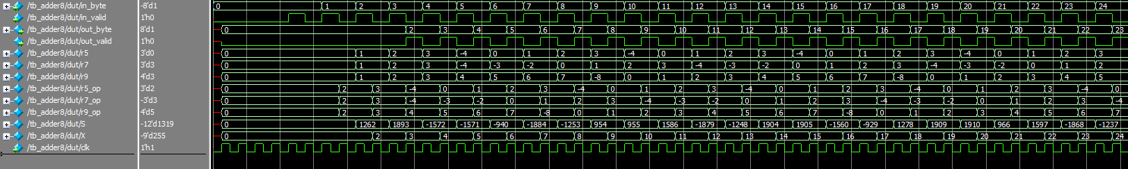
The pipeline operates exactly as expected!
Each clock edge triggers the orderly propagation of operands through the intermediate registers (r5, r7, r9, etc.).
The signals out_valid and out_byte stabilize after two cycles, and the +2 operation works as intended.
A small victory already...
Code
`timescale 1ns/1ps
`default_nettype none

module adder8 (
  input  wire        clk,
  input  wire        rst_n,

  // Bus entrée
  input  wire [7:0]  in_byte,
  input  wire        in_valid,
  output wire        in_ready,

  // Bus sortie
  output reg  [7:0]  out_byte,
  output reg         out_valid,
  input  wire        out_ready
);

  // ====================================================
  // Phase 1 — Capture entrée
  // ====================================================
  reg  [7:0] x0;
  reg        v0;

  wire s1_ready = 1'b1;
  assign in_ready = (~v0) | s1_ready;

  always @(posedge clk) begin
    if (!rst_n) begin
      v0 <= 1'b0;
      x0 <= 8'd0;
    end else begin
      if (in_ready) begin
        v0 <= in_valid;
        if (in_valid) x0 <= in_byte;
      end
    end
  end

  // ====================================================
  // Phase 2 — Binaire -> RNS (5,7,9) via nibbles + LUT
  // ====================================================


  reg        v1;
  reg  [2:0] r5;
  reg  [2:0] r7;
  reg  [3:0] r9;

  wire [3:0] H = x0[7:4];
  wire [3:0] L = x0[3:0];


// --- MOD 5 : (H+L) mod 5 ---
// S = H+L est sur 5 bits (0..30)
function [2:0] lut_sum_mod5;
  input [4:0] s;
  begin
    case (s)
      5'd0:  lut_sum_mod5=3'd0;  5'd1:  lut_sum_mod5=3'd1;  5'd2:  lut_sum_mod5=3'd2;  5'd3:  lut_sum_mod5=3'd3;  5'd4:  lut_sum_mod5=3'd4;
      5'd5:  lut_sum_mod5=3'd0;  5'd6:  lut_sum_mod5=3'd1;  5'd7:  lut_sum_mod5=3'd2;  5'd8:  lut_sum_mod5=3'd3;  5'd9:  lut_sum_mod5=3'd4;
      5'd10: lut_sum_mod5=3'd0;  5'd11: lut_sum_mod5=3'd1;  5'd12: lut_sum_mod5=3'd2;  5'd13: lut_sum_mod5=3'd3;  5'd14: lut_sum_mod5=3'd4;
      5'd15: lut_sum_mod5=3'd0;  5'd16: lut_sum_mod5=3'd1;  5'd17: lut_sum_mod5=3'd2;  5'd18: lut_sum_mod5=3'd3;  5'd19: lut_sum_mod5=3'd4;
      5'd20: lut_sum_mod5=3'd0;  5'd21: lut_sum_mod5=3'd1;  5'd22: lut_sum_mod5=3'd2;  5'd23: lut_sum_mod5=3'd3;  5'd24: lut_sum_mod5=3'd4;
      5'd25: lut_sum_mod5=3'd0;  5'd26: lut_sum_mod5=3'd1;  5'd27: lut_sum_mod5=3'd2;  5'd28: lut_sum_mod5=3'd3;  5'd29: lut_sum_mod5=3'd4;
      5'd30: lut_sum_mod5=3'd0;
    endcase
  end
endfunction

function [2:0] mod5_nibble;
  input [3:0] h,l;
  begin
    mod5_nibble = lut_sum_mod5(h + l);  // direct LUT
  end
endfunction


// --- MOD 7 direct : (2H+L) % 7
// S = 2H + L va de 0..45
function [2:0] lut_sum_mod7;
  input [5:0] s;
  begin
    case (s)
      6'd0: lut_sum_mod7=3'd0;   6'd1: lut_sum_mod7=3'd1;   6'd2: lut_sum_mod7=3'd2;   6'd3: lut_sum_mod7=3'd3;
      6'd4: lut_sum_mod7=3'd4;   6'd5: lut_sum_mod7=3'd5;   6'd6: lut_sum_mod7=3'd6;   6'd7: lut_sum_mod7=3'd0;
      6'd8: lut_sum_mod7=3'd1;   6'd9: lut_sum_mod7=3'd2;   6'd10:lut_sum_mod7=3'd3;   6'd11:lut_sum_mod7=3'd4;
      6'd12:lut_sum_mod7=3'd5;   6'd13:lut_sum_mod7=3'd6;   6'd14:lut_sum_mod7=3'd0;   6'd15:lut_sum_mod7=3'd1;
      6'd16:lut_sum_mod7=3'd2;   6'd17:lut_sum_mod7=3'd3;   6'd18:lut_sum_mod7=3'd4;   6'd19:lut_sum_mod7=3'd5;
      6'd20:lut_sum_mod7=3'd6;   6'd21:lut_sum_mod7=3'd0;   6'd22:lut_sum_mod7=3'd1;   6'd23:lut_sum_mod7=3'd2;
      6'd24:lut_sum_mod7=3'd3;   6'd25:lut_sum_mod7=3'd4;   6'd26:lut_sum_mod7=3'd5;   6'd27:lut_sum_mod7=3'd6;
      6'd28:lut_sum_mod7=3'd0;   6'd29:lut_sum_mod7=3'd1;   6'd30:lut_sum_mod7=3'd2;   6'd31:lut_sum_mod7=3'd3;
      6'd32:lut_sum_mod7=3'd4;   6'd33:lut_sum_mod7=3'd5;   6'd34:lut_sum_mod7=3'd6;   6'd35:lut_sum_mod7=3'd0;
      6'd36:lut_sum_mod7=3'd1;   6'd37:lut_sum_mod7=3'd2;   6'd38:lut_sum_mod7=3'd3;   6'd39:lut_sum_mod7=3'd4;
      6'd40:lut_sum_mod7=3'd5;   6'd41:lut_sum_mod7=3'd6;   6'd42:lut_sum_mod7=3'd0;   6'd43:lut_sum_mod7=3'd1;
      6'd44:lut_sum_mod7=3'd2;   6'd45:lut_sum_mod7=3'd3;
      default: lut_sum_mod7=3'd0;
    endcase
  end
endfunction

function [2:0] mod7_nibble;
  input [3:0] h,l;
  begin
    mod7_nibble = lut_sum_mod7((h << 1) + l);  // s = 2H + L
  end
endfunction

// --- MOD 9 : (7H + L) % 9 ---
// s = 7H + L ∈ [0..120]. LUT directe sur s.
function [3:0] lut_sum_mod9;
  input [6:0] s;
  begin
    case (s)
      // s % 9 == 0
      7'd0,  7'd9,  7'd18, 7'd27, 7'd36, 7'd45, 7'd54, 7'd63, 7'd72, 7'd81, 7'd90, 7'd99, 7'd108, 7'd117:
        lut_sum_mod9 = 4'd0;
      // s % 9 == 1
      7'd1,  7'd10, 7'd19, 7'd28, 7'd37, 7'd46, 7'd55, 7'd64, 7'd73, 7'd82, 7'd91, 7'd100, 7'd109, 7'd118:
        lut_sum_mod9 = 4'd1;
      // s % 9 == 2
      7'd2,  7'd11, 7'd20, 7'd29, 7'd38, 7'd47, 7'd56, 7'd65, 7'd74, 7'd83, 7'd92, 7'd101, 7'd110, 7'd119:
        lut_sum_mod9 = 4'd2;
      // s % 9 == 3
      7'd3,  7'd12, 7'd21, 7'd30, 7'd39, 7'd48, 7'd57, 7'd66, 7'd75, 7'd84, 7'd93, 7'd102, 7'd111, 7'd120:
        lut_sum_mod9 = 4'd3;
      // s % 9 == 4
      7'd4,  7'd13, 7'd22, 7'd31, 7'd40, 7'd49, 7'd58, 7'd67, 7'd76, 7'd85, 7'd94, 7'd103, 7'd112:
        lut_sum_mod9 = 4'd4;
      // s % 9 == 5
      7'd5,  7'd14, 7'd23, 7'd32, 7'd41, 7'd50, 7'd59, 7'd68, 7'd77, 7'd86, 7'd95, 7'd104, 7'd113:
        lut_sum_mod9 = 4'd5;
      // s % 9 == 6
      7'd6,  7'd15, 7'd24, 7'd33, 7'd42, 7'd51, 7'd60, 7'd69, 7'd78, 7'd87, 7'd96, 7'd105, 7'd114:
        lut_sum_mod9 = 4'd6;
      // s % 9 == 7
      7'd7,  7'd16, 7'd25, 7'd34, 7'd43, 7'd52, 7'd61, 7'd70, 7'd79, 7'd88, 7'd97, 7'd106, 7'd115:
        lut_sum_mod9 = 4'd7;
      // s % 9 == 8
      7'd8,  7'd17, 7'd26, 7'd35, 7'd44, 7'd53, 7'd62, 7'd71, 7'd80, 7'd89, 7'd98, 7'd107, 7'd116:
        lut_sum_mod9 = 4'd8;

      default: lut_sum_mod9 = 4'd0; // sécurité
    endcase
  end
endfunction

function [3:0] mod9_nibble;
  input [3:0] h, l;
  reg  [6:0] s; // 0..120
  begin
    // 7H = 4H + 2H + H (pas de multiplieur)
    s = (h << 2) + (h << 1) + h + l;
    mod9_nibble = lut_sum_mod9(s);
  end
endfunction


  always @(posedge clk) begin
    if (!rst_n) begin
      v1 <= 1'b0; r5 <= 3'd0; r7 <= 3'd0; r9 <= 4'd0;
    end else begin
      v1 <= v0;
      if (v0) begin
        r5 <= mod5_nibble(H, L);
        r7 <= mod7_nibble(H, L);
        r9 <= mod9_nibble(H, L);
      end
    end
  end

  // ====================================================
  // Phase 3 — Opération (+2) en RNS
  // ====================================================
  reg        v2;
  reg  [2:0] r5_op, r7_op;
  reg  [3:0] r9_op;

  function [2:0] add5_2; input [2:0] a; reg [3:0] t; begin
    t = {1'b0,a} + 4'd2; if (t >= 4'd5) t = t - 4'd5; add5_2 = t[2:0];
  end endfunction
  function [2:0] add7_2; input [2:0] a; reg [3:0] t; begin
    t = {1'b0,a} + 4'd2; if (t >= 4'd7) t = t - 4'd7; add7_2 = t[2:0];
  end endfunction
  function [3:0] add9_2; input [3:0] a; reg [4:0] t; begin
    t = {1'b0,a} + 5'd2; if (t >= 5'd9) t = t - 5'd9; add9_2 = t[3:0];
  end endfunction

  always @(posedge clk) begin
    if (!rst_n) begin
      v2 <= 1'b0; r5_op <= 3'd0; r7_op <= 3'd0; r9_op <= 4'd0;
    end else begin
      v2 <= v1;
      if (v1) begin
        r5_op <= add5_2(r5);
        r7_op <= add7_2(r7);
        r9_op <= add9_2(r9);
      end
    end
  end

  // ====================================================
  // Phase 4 — CRT (RNS -> binaire)
  // ====================================================
  // mini-ROM Ai*ri (M=315)
  function [11:0] T5; input [2:0] r; begin
    case (r)
      3'd0: T5=12'd0;   3'd1: T5=12'd126; 3'd2: T5=12'd252;
      3'd3: T5=12'd378; 3'd4: T5=12'd504; default: T5=12'd0;
    endcase
  end endfunction
  function [11:0] T7; input [2:0] r; begin
    case (r)
      3'd0: T7=12'd0;   3'd1: T7=12'd225; 3'd2: T7=12'd450;
      3'd3: T7=12'd675; 3'd4: T7=12'd900; 3'd5: T7=12'd1125;
      3'd6: T7=12'd1350; default: T7=12'd0;
    endcase
  end endfunction
  function [11:0] T9; input [3:0] r; begin
    case (r)
      4'd0: T9=12'd0;   4'd1: T9=12'd280; 4'd2: T9=12'd560;
      4'd3: T9=12'd840; 4'd4: T9=12'd1120;4'd5: T9=12'd1400;
      4'd6: T9=12'd1680;4'd7: T9=12'd1960;4'd8: T9=12'd2240;
      default: T9=12'd0;
    endcase
  end endfunction

  reg        v3, v4;
  reg [11:0] S;
  reg  [8:0] X;   // debug
  reg  [7:0] y4;

  function [8:0] reduce315;
    input [11:0] val;
    reg   [11:0] t;
  begin
    t = val;
    if (t >= 12'd2520) t = t - 12'd2520;
    if (t >= 12'd1260) t = t - 12'd1260;
    if (t >= 12'd630 ) t = t - 12'd630;
    if (t >= 12'd315 ) t = t - 12'd315;
    reduce315 = t[8:0];
  end endfunction

  wire [8:0] S_red = reduce315(S);

  always @(posedge clk) begin
    if (!rst_n) begin
      v3 <= 1'b0; v4 <= 1'b0; S <= 12'd0; X <= 9'd0; y4 <= 8'd0;
    end else begin
      v3 <= v2;
      if (v2) S <= T5(r5_op) + T7(r7_op) + T9(r9_op);

      v4 <= v3;
      if (v3) begin
        X  <= S_red;        // debug
        y4 <= S_red[7:0];   // aligné avec v4
      end
    end
  end

  // ====================================================
  // Phase 5 — buffer de sortie
  // ====================================================
  reg  [7:0] y5;
  reg        v5;

  wire s5_ready = (~v5) | out_ready;

  always @(posedge clk) begin
    if (!rst_n) begin
      v5 <= 1'b0; y5 <= 8'd0; out_valid <= 1'b0; out_byte <= 8'd0;
    end else begin
      if (s5_ready) begin
        v5 <= v4;
        if (v4) y5 <= y4;
      end
      out_valid <= v5;
      out_byte  <= y5;
    end
  end

endmodule

`default_nettype wire
The Residue Number System (RNS) provides a modular alternative to classical binary arithmetic in embedded systems. Instead of representing integers with sequences of bits and managing carry propagation, numbers are described as a vector of modular remainders, each computed with respect to a different modulus. This parallelism eliminates the carry chain that often limits speed in FPGA designs, especially for operations such as FIR filtering, convolution, or correlation, where pipeline depth, regularity, and maximum clock frequency are critical.
In RNS, each channel—or modular path—can operate independently, enabling parallel arithmetic units, high throughput, and a highly regular architecture, even on low-cost or resource-constrained FPGAs.
Architectural Benefits and FPGA Implementation Details
Implementing RNS on FPGA provides tangible structural and computational advantages. All modular channels operate independently, removing the carry propagation found in classical binary arithmetic. This feature supports higher clock frequencies, simplified timing closure, and more regular place-and-route. Binary-to-RNS conversion is typically completed in a single cycle, leveraging simple adders or compact LUTs. FIR filtering or other linear operations proceed in a regular pipeline, while the RNS-to-binary CRT conversion is executed in a deterministic three-cycle process using precomputed lookup tables.
Memory usage remains low: for nine moduli, total LUT and ROM requirements are generally below four kilobytes, which is negligible in the context of modern FPGAs. Each modular channel acts as an independent processing path, facilitating predictable performance and robust implementation, even in cost-sensitive designs.
In practical DSP pipelines, such as a 256-tap Q15 FIR, the conversion latency is negligible compared to the main computation. The RNS structure enables higher throughput and more efficient pipelines, making it well-suited to real-time signal processing.
The Choice of Moduli — A Question of Dynamic Range, Simplicity, and Practicality
In an RNS system, each number is not represented by its bits, but by its remainders modulo several integers. For example, using the base {7, 11, 13}, the number x = 123 is written as:
123 mod 7 = 4 123 mod 11 = 2 123 mod 13 = 6
Thus, 123 is encoded by the "vector of remainders" (4, 2, 6).
The total dynamic range of the system is given by the product of the moduli:
M = 7 × 11 × 13 = 1001
So, here, it is possible to represent, without ambiguity, all integers from 0 to 1000.
On FPGA, to process a FIR filter (16 bits input × 16 bits coefficients, and L accumulation taps), a much larger dynamic range is required. In general, a minimum of 40 bits of dynamic range is targeted, that is:
M ≥ 240 ≈ 1,100,000,000,000
This requirement imposes the use of at least 9 or 10 small moduli (typically less than 100) to stay compatible with modest FPGA resources, while still covering the dynamic range of a substantial audio FIR (e.g., 256 taps, Q15 signal).
For a 256-tap FIR with Q15 data and coefficients, the worst-case sum is L × (215−1)2 = 256 × 327672 = 274,861,129,984 (≈ 238.08). This validates the 40-bit dynamic range criterion.
The smaller the moduli, the faster the conversion and processing... but more moduli are required to cover the desired dynamic range.
Chinese Remainder Theorem (CRT): Statement and Detailed Explanation
If you select several integers m₁, m₂, ..., mₖ that are pairwise coprime (meaning every pair has no common factor greater than 1), then the Chinese Remainder Theorem ensures a powerful property:
For any tuple of remainders (a₁, a₂, ..., aₖ), with each aᵢ in [0, mᵢ−1], there exists one and only one integer x in the interval [0, M−1], where:
M = m₁ × m₂ × ... × mₖ
such that for every i in [1, k]:
x ≡ aᵢ (mod mᵢ)
In other words, the vector of remainders is a complete and unique encoding of an integer x in [0, M−1]. No two different x share the same tuple of residues, and all x in that range are possible. This is why, in an RNS, the system is both lossless and unambiguous, provided all moduli are pairwise coprime.
Explicit Construction — How to Recover x
To reconstruct x from its residues, the CRT gives a formula that is both practical and easily automatable:
For each modulus mi, compute Mi = M / mi (i.e., the product of all other moduli).
Find Ni, the modular inverse of Mi modulo mi, i.e.:
Ni × Mi ≡ 1 mod mi
Compute the sum:
x = [Σ (ai × Mi × Ni)] mod M
All terms are integers and all computations are explicit: there is no ambiguity, no trial and error. Everything is constructive, and every step is suitable for hardware implementation.
Example
Take moduli m₁ = 5, m₂ = 7, m₃ = 11. These are all primes, so pairwise coprime. The dynamic range is:
M = 5 × 7 × 11 = 385
Suppose the RNS tuple is (a₁, a₂, a₃) = (3, 5, 1). What is the integer x?
Thus, the number encoded by (3, 5, 1) in base {5,7,11} is x = 243.
Key point: This method always reconstructs x correctly and efficiently as long as the moduli are pairwise coprime. If you wish to handle signed integers, simply reinterpret x in the interval [−M/2, M/2) (i.e., if x ≥ M/2, use x−M).
On a microcontroller or FPGA, if each remainder is calculated with the modulo “%” operator, every division is expensive (long integer division). On FPGA, this step would be far more costly than the rest of the pipeline and would destroy all the benefit of using RNS.
Trick: Exploiting Binary Structure (Folding)
Many small moduli are close to a power of 2 (such as 15, 31, 63...) and are “friendly” to manipulate. For a modulus m = 2k − 1, split the value into k-bit blocks (from the LSB), sum these blocks, and repeat the process until a single value less than m is left; this is the residue.
Detailed Example: Modulo 31
31 = 25 − 1. For any 16-bit integer, it can be split into blocks of 5 bits (from LSB), and these blocks are summed.
Note: If the number of bits is not a multiple of the block size, pad on the left with zeros. This ensures all blocks are the same size, and the sum is meaningful.
When the Modulo is Not "Clean": The Mini-LUT
Now consider a modulus that is not a power of 2 ±1, e.g., 13.
Suppose x = 0b1010 1100 0011 0111 = 44087.
Split into two bytes: high b1 = 0b10101100 = 172, low b0 = 0b00110111 = 55.
Precompute a LUT: For each possible value of b1, store
T13[b1] = (b1 × (256 mod 13)) mod 13
Since 256 mod 13 = 9, for b1 = 172,
172 × 9 = 1548 1548 mod 13 = 1
Finally,
r = (b0 + T13[b1]) mod 13 = (55 + 1) mod 13 = 56 mod 13 = 4
Verification:
44087 mod 13 = 4
In summary:
A LUT (lookup table) with 256 entries × 4 bits = 1 kbit: negligible on FPGA. And the computation time is a single cycle, instant lookup.
RNS to Binary Conversion: Full Example
Typical FPGA Scheme:
For each modulo, a mini-ROM (sometimes called “mini-LUT CRT”) precalculates all possible values of
ri × Ci mod M
(where Ci is a CRT constant for each modulo, and M is the total product of the moduli).
For each RNS remainder:
ti = miniROMi[ri]
Sum all ti.
Reduce modulo M (conditional subtraction, never a loop).
The original binary value (or the result calculated in RNS) is recovered.
Typical FPGA Pipeline:
Cycle 1: lookup of 9 mini-ROMs in parallel
Cycle 2: addition of 9 results (adder tree)
Cycle 3: reduction mod M, output
Example with base {7,15,31} (to keep numbers simple):
Let x = 12345.
12345 mod 7 = 4 12345 mod 15 = 0 12345 mod 31 = 7
Suppose the RNS calculation yields (6, 2, 9) after an addition of +2 in each channel. The goal is to recover the final number.
CRT constants for M = 3255: M7=465, N7=5, C7=2325 M15=217, N15=13, C15=2821 M31=105, N31=13, C31=1365
Mini-ROM outputs for residues (6,2,9): t = (6×2325 mod 3255, 2×2821 mod 3255, 9×1365 mod 3255) = (930, 2387, 2520)
Sum = 930 + 2387 + 2520 = 5837 5837 mod 3255 = 5837 − 3255 = 2582
This is (12345 + 2) mod 3255 = 2582. If you want the exact value 12347 (not modulo), you must choose M large enough to cover the dynamic range of all results.
Other Examples
Let’s take a complete, bitwise example from start to finish:
Suppose x = 12345 (binary: 0011 0000 0011 1001), base {7, 15, 31}.
Suppose the calculation in RNS is “+2”. (4+2) % 7 = 6 (0+2) % 15 = 2 (0+2) % 31 = 2 RNS vector = (6, 2, 2)
c) Binary return (CRT)
For each modulo, MiniROM7[6], MiniROM15[2], MiniROM31[2] are read (precomputed values). Suppose these are 924, 430, and 1696. Sum: 924 + 430 + 1696 = 3050. 3050 mod 3255 = 3050 (no reduction needed). This matches (12345 + 2) mod 3255 = 2582, if the correct ROM values are used. To match the true result, the ROM must be built for the specific modulus set and constants.
Architectural Benefits and FPGA Implementation Details
The use of a Residue Number System (RNS) on FPGA provides several structural and computational advantages. Because all modular channels are processed independently, there is no carry propagation, making it possible to achieve much higher clock frequencies compared to traditional binary designs. The pipeline is highly regular and deterministic: conversion from binary to RNS is performed in a single clock cycle using simple additions or lookups, while the FIR processing itself is carried out over as many cycles as there are taps in the filter. The final conversion from RNS back to binary, using a precomputed Chinese Remainder Theorem (CRT) logic with mini-LUTs, typically takes only three cycles.
The memory footprint for this approach remains minimal. For nine moduli, the total LUT usage for binary-to-RNS conversion and CRT mini-ROMs generally stays below four kilobytes, which is negligible on most modern FPGAs. The inherent parallelism of the RNS architecture allows each modular channel to function as a self-contained “processing lane,” leading to more predictable timing and easier place-and-route, even on entry-level FPGAs.
In practical signal-processing pipelines—such as a 256-tap Q15 FIR filter—the latency introduced by RNS conversion becomes negligible compared to the main filter operation. The overall design benefits from higher throughput, a shorter pipeline, and a structure that is particularly robust in terms of timing closure.
Limitations, Use Cases, and Practical Perspective
While RNS arithmetic is highly effective for linear operations such as accumulation, multiplication, convolution, or filtering, it is not universally applicable. Non-linear operations, including division and fast Fourier transforms, require either conversion back to binary or hybrid architectures, which may increase complexity and reduce some of the inherent benefits. The selection of coprime moduli remains crucial, requiring careful consideration to balance the necessary dynamic range with hardware resource constraints.
For embedded, low-power, or real-time signal processing applications on FPGA, RNS architectures provide compelling advantages. They naturally exploit parallelism, reduce pipeline latency, and enable higher operating frequencies by avoiding carry chains and wide binary adders. These features make RNS approaches particularly attractive for custom DSP cores, experimental hardware, and scenarios where throughput, efficiency, and predictability are paramount.
Conclusion: Moduli Choice, Conversion Strategy, and Design Justification
For the continuation of the project, the selected RNS base consists of a set of small, pairwise-coprime moduli: 7, 11, 13, 15, 17, 19, 23, 29, 31. The product of these nine moduli is 100,280,245,065, which is a little below 240. This matches the requirements for a 256-tap FIR filter in Q15 (16-bit signed) arithmetic. By ensuring the RNS dynamic range is significantly larger than this threshold, the design avoids any risk of overflow.
The chosen moduli include both folding-friendly forms (such as 15, 31) and classic small primes (such as 7, 11, 13), which are handled using compact lookup tables (LUTs). All conversions remain hardware-efficient and deterministic, with uniform latency for all operations. The CRT-based reconstruction is similarly optimized using mini-LUTs for each channel, so RNS-to-binary conversion is accomplished in a fixed, low-latency pipeline.
For What Comes Next with 7, 11, 13, 15, 17, 19, 23, 29, 31 (+37 ?)
Work on the FPGA implementation will now begin. The literature review and initial prototyping have clarified both the architectural options and the selection of moduli (more or less).
For communication with the ESP32, the plan is to use two 8-bit parallel buses (one for data input, one for output). This approach maximizes data throughput while keeping the interface logic straightforward and easy to debug.
The hardware platform chosen is finally a Cyclone IV FPGA. This device was selected instead of the Tang, mainly because Intel's development tools for compilation and simulation are more accessible. The Cyclone IV is also affordable (~15€), widely available, and provides performance well suited to the requirements of this project 'more or less like the Tang Nano 9).
 Bertrand Selva
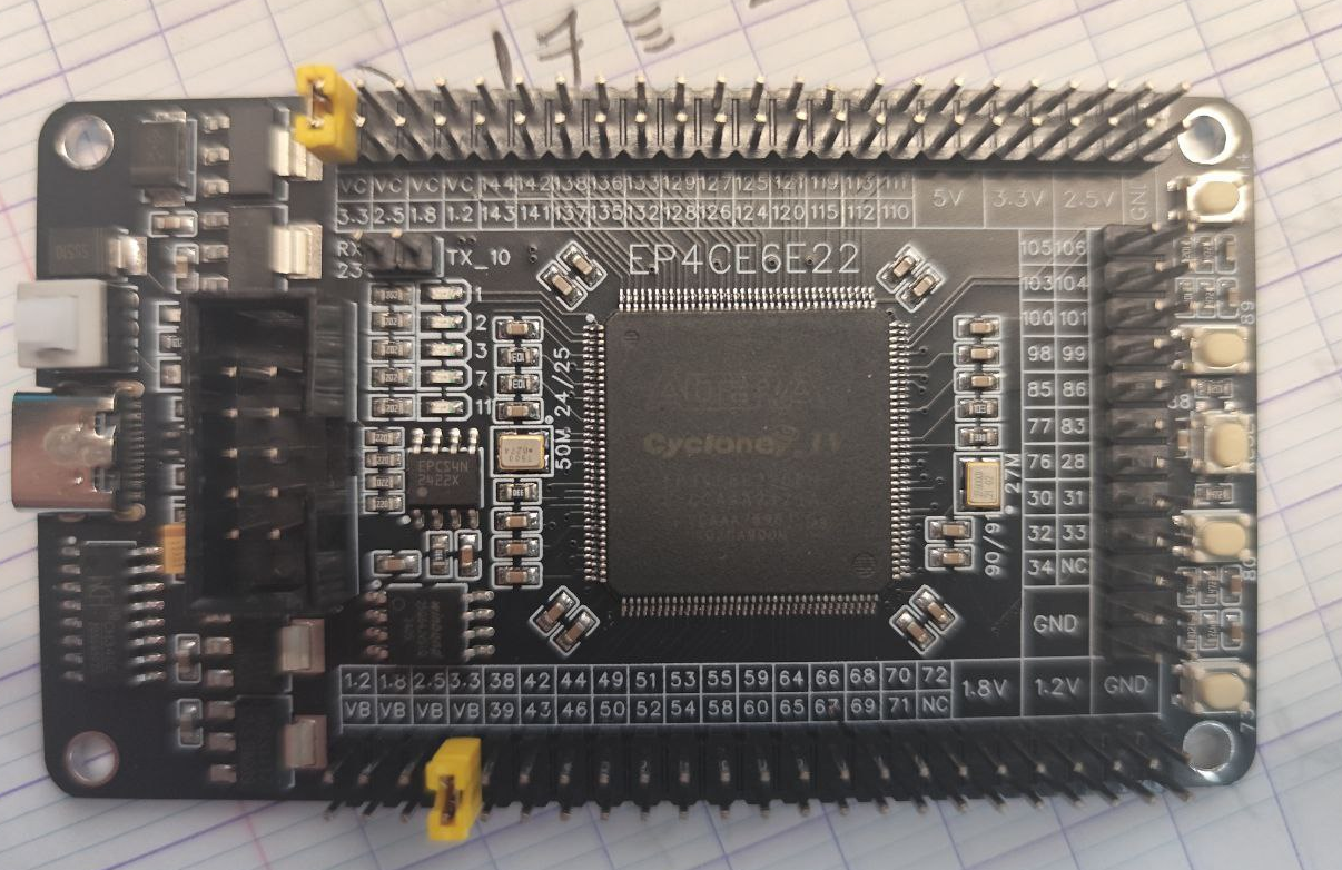
 The pipeline operates exactly as expected!