Close
0%
0%

Winter, FPGAs, and Forgotten Arithmetic

RNS on FPGA: Revisiting an Unusual Number System for Modern Signal Processing

Similar projects worth following
Winter is coming.
No more tinkering outdoors, no more demanding builds in the cold workshop.
Like marmots and bears — if only they had PCs — I’ll be hibernating behind my screen.
So I needed a project that fits this new pace.
I’ve been meaning to get into FPGA development for quite a while. But the usual “educational” examples always turned me off: blinking a LED or writing a counter never really excited me.
This time, I’ve found a much more inspiring thread to follow: implementing RNS-based FIR filtering on FPGA (cold war inspiration).
Meanwhile, my "LoRaTube" project is currently on hold — I’m waiting for the hardware.

The Inspiration: Duga and the mysterious K340A

I recently stumbled upon some urban exploration photos from the Duga radar site near Chernobyl and an excellent documentary video : (www.youtube.com/watch?v=kHiCHRB-RlA&t=605s).
This gigantic over-the-horizon radar, made of hundreds of antennas, is famous for its distinctive shortwave noise — the “Russian Woodpecker” — that annoyed ham radio operators in the ‘70s and ‘80s.

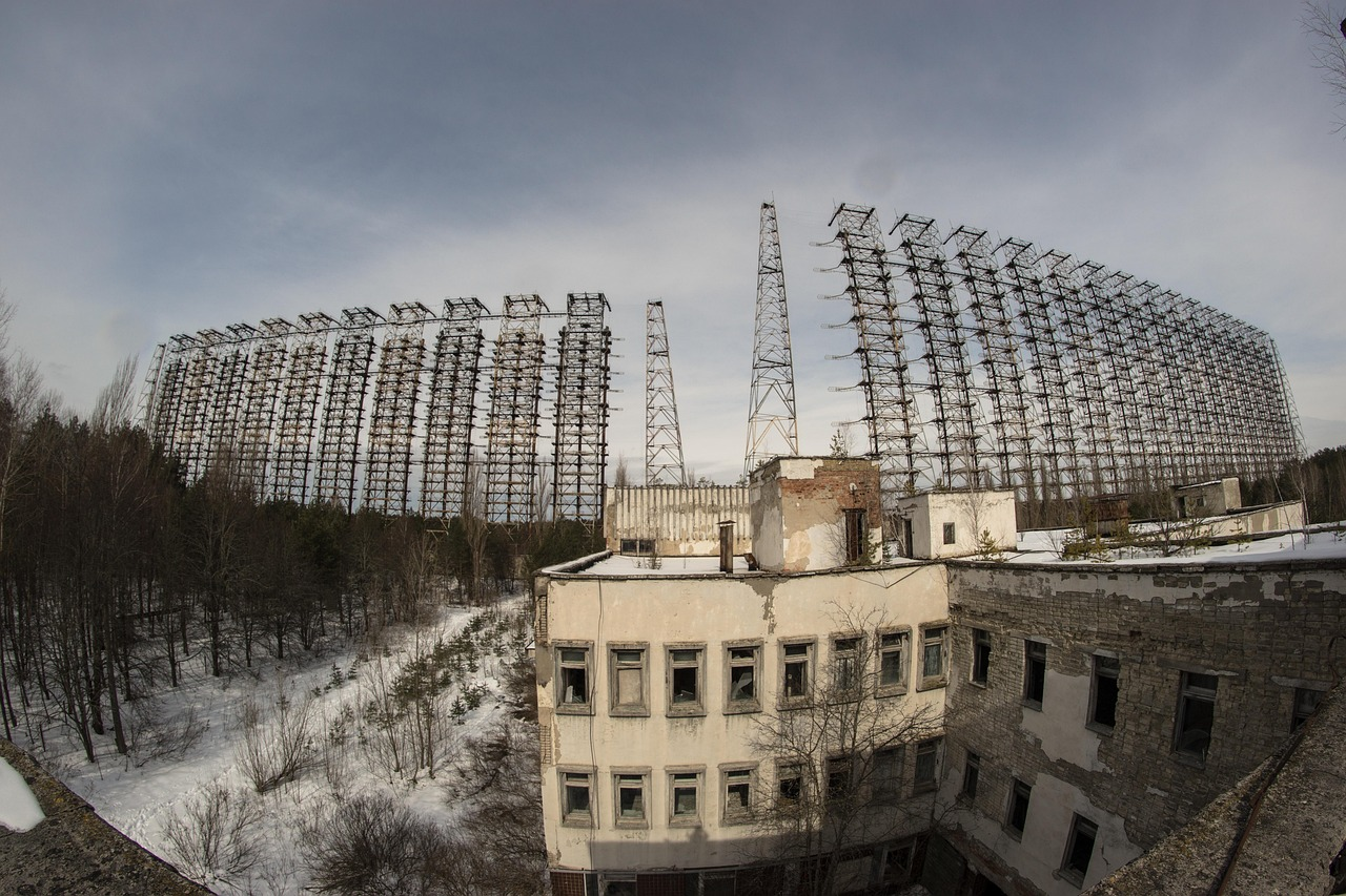
Among the pictures, one can still spot a massive computer left inside the abandoned building: the K340A.
Not your average 1970s computer.

Back then, the USSR was lagging behind in microelectronics. To process the data streams from such a large radar, engineers had to invent clever architectures. The K340A used a very peculiar number system: the Residue Number System (RNS).

A Brief Mathematical Detour: What is RNS?

The idea is surprisingly old (Chinese Remainder Theorem, ~3rd century):

  • Instead of representing numbers in binary, you use their remainders modulo several pairwise coprime bases.

  • For example, using moduli (3, 5, 7), the number 23 becomes (2, 3, 2).

  • You can add or multiply component-wise, independently — no carry, no dependencies.

It’s parallel by design. That’s what made it such a good fit for hardware with limited logic.

At the time, this offered a massive gain in logic simplicity and parallelism. Very clever engineering…

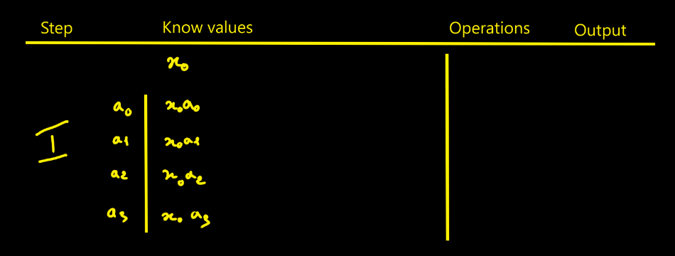
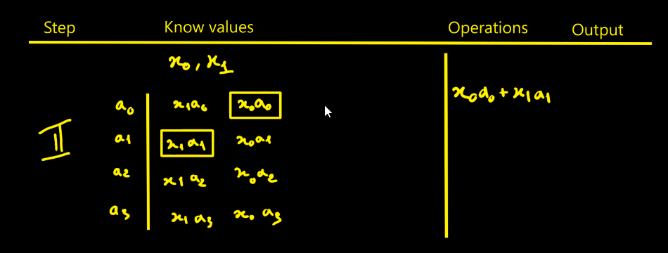
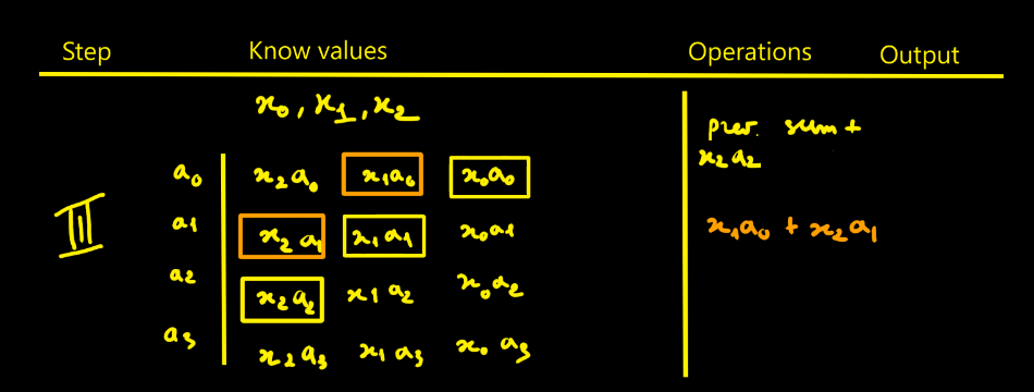
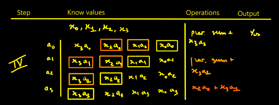
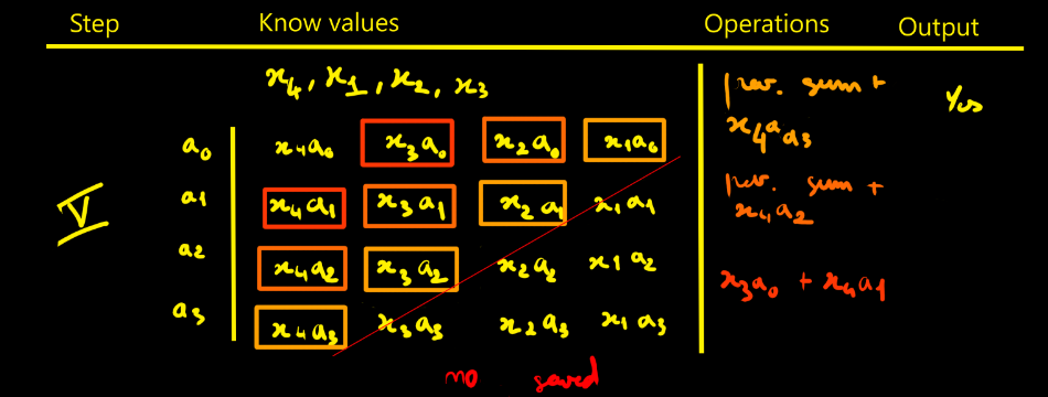
To convert back to a standard value, you apply the Chinese Remainder Theorem (CRT):

N = ∑ rᵢ ⋅ Mᵢ ⋅ yᵢ mod M

Where M is the product of all moduli, Mᵢ = M / mᵢ, and yᵢ is the modular inverse of Mᵢ.

In practice, this back-conversion is costly — that’s why systems like the K340A only used CRT when strictly necessary, e.g., to display human-readable output.
All radar processing (correlation, FIR, FFT) stayed entirely in RNS.

Why is RNS interesting today?

In the Cold War era, RNS offered a way to perform fast and parallel calculations with minimal hardware.

Nowadays, we live in a very different context. FPGA chips are binary-optimized, with built-in DSP slices and accumulators. So… why go back to RNS?

Well, first of all — because it’s cool. There’s something fascinating about rediscovering the strange and beautiful architectures of the Cold War. But there’s more to it than that.

RNS fits surprisingly well with the constraints of modern embedded systems: low-power, compact, robust, and predictable architectures.

Let’s take a closer look.

With RNS:

  • There’s no carry chain — additions don’t ripple. Logic is simpler, timing is tighter, and power usage is lower.

  • It scales naturally — instead of increasing bus width, you just add another modulo.

  • It can be fault-tolerant — a failing modulo can often be detected (or even corrected) thanks to redundancy.

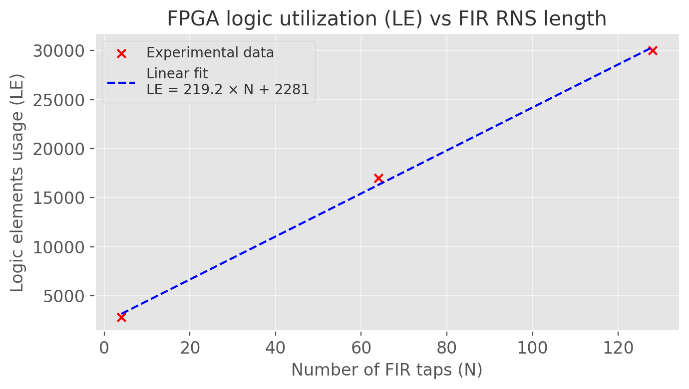
  • It saves energy — instead of deep binary adders, you can build flat parallel modulo lanes that burn fewer LUTs. The architecture is (maybe) more efficient.

  • It’s a fresh perspective — in a binary-dominated world, revisiting RNS is like exploring a parallel timeline in computing.

Could we actually see energy savings in a small demonstrator? That’s one of the questions I want to explore here.

This also resonates with modern applications like:

  • frugal DSP (e.g., filters, radar processing),

  • lightweight cryptography (modular arithmetic, side-channel resistance),

  • embedded AI (where matrix (addition and multiplication) operations dominate and average precision is often enough).

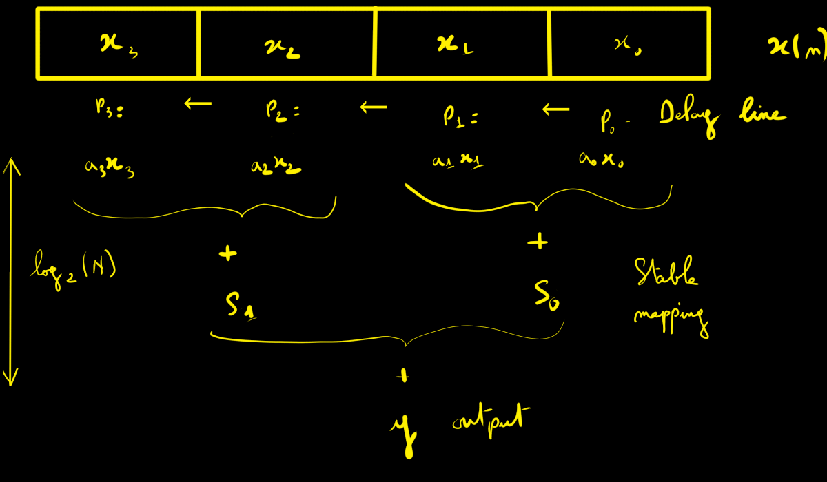
The Project: A Modern RNS DSP Filter

I want to reimplement a basic signal processing chain using RNS, on accessible, modern hardware.

Here’s the plan:

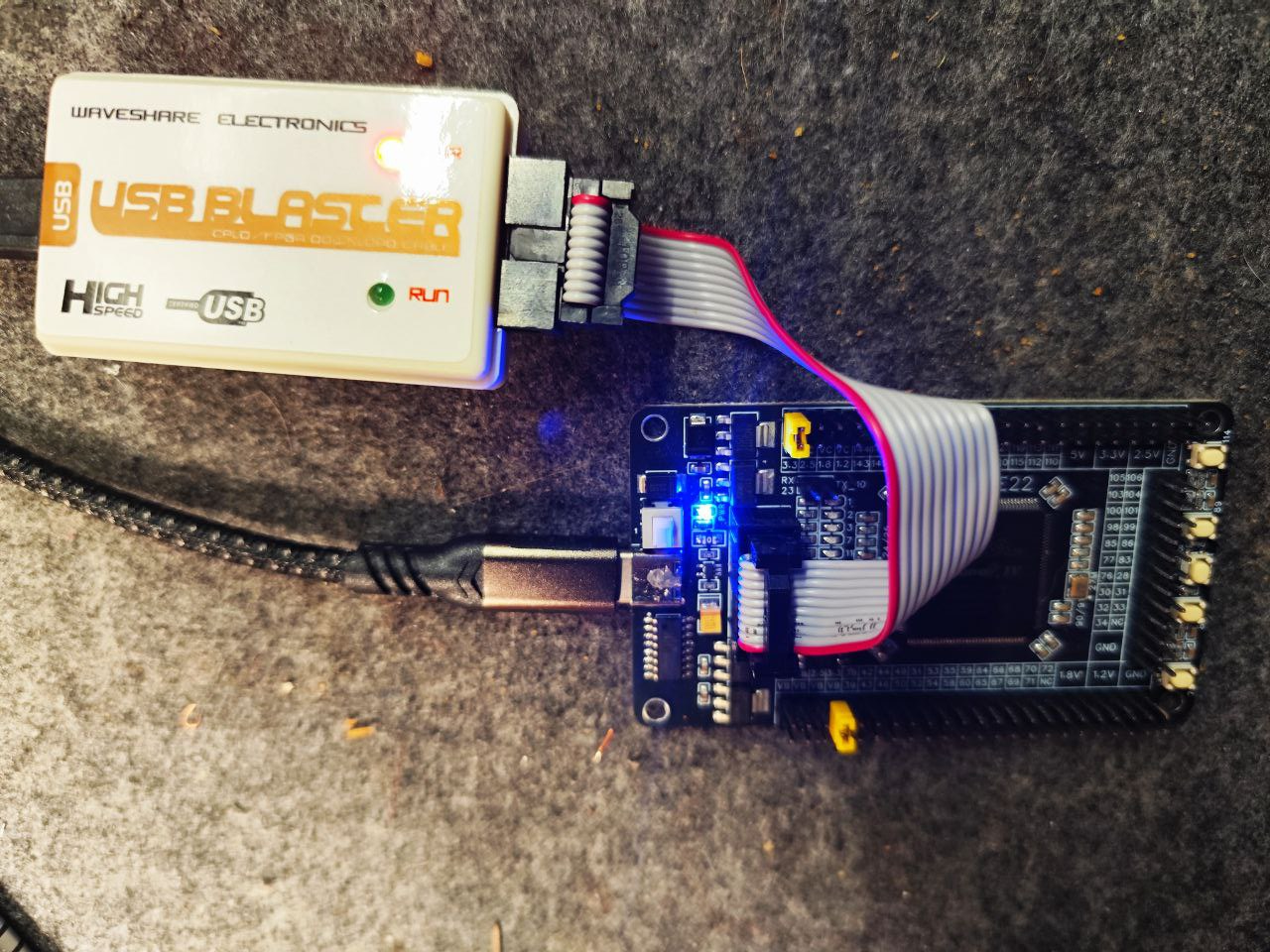
  • I’ll use a Tang Nano 9K (GW1N-9) FPGA to wire up the RNS logic.

  • It will work alongside an ESP32-S3 that handles I/O and orchestration.

Why this setup? Because it's cheap, well-documented, and popular in the maker community. And because I know almost nothing about...

Read more »

PROGRAMME16BITS_FIRCOMPLET64TAPS_BACKPRESSURE.zip

64 TAPS RNS FIR WITH BACKPRESSURE

x-zip-compressed - 31.90 MB - 11/16/2025 at 14:33

Download

PROGRAMME16BITS_FIRCOMPLET64TAPS.zip

64 TAPS RNS FIR

x-zip-compressed - 31.95 MB - 11/10/2025 at 16:06

Download

PROGRAMME16BITS_FIRCOMPLET.zip

4 TAPS RNS FIR

x-zip-compressed - 19.70 MB - 11/09/2025 at 17:38

Download

lut_verilog.v

These functions multi<modulus>_h<tap> encodes the multiplication table (h_int[tap] * r) % modulus

v - 885.81 kB - 10/23/2025 at 19:01

Download

  • BACKPRESSURE

    Bertrand Selva11/16/2025 at 14:31 0 comments

    Implementing Backpressure in a No-RAM Pipeline

    In the latest version of the project (see attached source), I've introduced a simple backpressure mechanism to ensure that each produced data word is truly consumed before a new one is accepted. Here’s how it works:

    The design is 100% synchronous. There is no external RAM, no FIFO. The objectives are twofold:
    – Never overwrite an output that hasn’t yet been read.
    – Never accept a new input until the previous output is consumed.
    For debugging and visualization, the 16 output bits will be connected to a parallel bus, monitored by the logic analyzer.

    Validation Protocol

    The pipeline uses two standard handshake signals:
    out_valid: signals that output data is ready.
    out_ready: external pulse signaling the data has been consumed.
    Control logic is built around:
    wire hold_pipeline = (out_valid && !out_ready);
    wire step_en = !hold_pipeline;
    Pipeline steps forward only if the previous output has been read (out_ready=1). Otherwise, the pipeline is frozen everywhere. The step_en signal then drives all internal enables.
    This logic ensures:
    – No new input if previous output isn’t consumed.
    – No risk of internal overflow, even with zero FIFO.
    – The pipeline remains frozen as long as downstream isn’t ready.
    That’s exactly what’s needed for streaming scenarios controlled by a slow peripheral or manual inspection.

    Signal Legend

    SignalDirectionRole/Meaning
    in_validInputExternal → FPGA: “Input data is present on in_byte”
    in_readyOutputFPGA → External: “I can accept a new input now”
    in_byteInputExternal → FPGA: Data to process (8 bits)
    out_wordOutputFPGA → External: Output word produced (16 bits)
    out_validOutputFPGA → External: “Output data is ready, read me!”
    out_readyInputExternal → FPGA: “The output data has just been read/consumed”

    Typical Timing

    cyclein_validin_readyout_wordout_validout_readyDescription
    001--01 Idle state. FPGA does nothing—no input pending, no output produced. in_ready=1: ready to accept. out_valid=0: nothing to read. The outside can inject a value at any time.
    111X110 Input received. External presents value on in_byte with in_valid=1 (pipeline ready). The pipeline captures input, computes, produces X1, sets out_valid=1. out_ready=0: output not yet consumed.
    200X110 Waiting for consumption. Input transfer done (in_valid=0), output not yet read (out_ready=0). Pipeline blocks: in_ready=0, out_valid=1, output is held stable. Registers frozen, no updates.
    300X111 Output read. External acknowledges output by asserting out_ready=1 for one cycle. The pipeline sees the "green light": data is consumed. X1 is readed by ESP32. On next clock, pipeline will advance and be ready for new input.
    001X101 Return to idle. After data consumption, pipeline returns to idle: in_ready=1, ready to accept a new word. Cycle repeats as above for the next input.
    111X210 New input accepted. External detects in_ready=1 and injects a new value with in_valid=1. The pipeline captures this new input, computes X2, and outputs it. Sequence is analogous to step 1.

    Key Principles

    • Computation (internal register update) happens only on a clock edge where step_en=1, i.e.:
      step_en = !hold_pipeline = !(out_valid && !out_ready)
    • If the output is not consum hold_pipeline and step_en depending on the statesed (out_ready=0), the entire pipeline is frozen: no new input, no state evolution, everything held stable.
    • in_ready=1 only when the pipeline can accept a new input (never if the previous output remains unconsumed).
    • The external system dictates the pace: as long as out_ready isn't asserted, there is no risk of data loss or overflow, as the pipeline remains frozen. The external master sets the tempo.

    hold_pipeline and step_en depending on the states

    In the idle state, the pipeline keeps stepping on every clock edge, because step_en = 1 as long as out_valid = 0.
    But in_fire = in_valid && in_ready stays at 0, since...

    Read more »

  • USB BLASTER V2 OK

    Bertrand Selva11/15/2025 at 19:27 0 comments

    I had bought a USB Blaster on AliExpress for 2€.

    If it had worked, it would have been great…

    I tried it with Quartus 13 and Quartus 22. Nothing worked: it just wouldn’t function.

    So I bought a Waveshare Electronics USB Blaster V2, and this time my FPGA was detected immediately and everything worked on the first try with Quartus 22.

    I paid around thirty euros for this version, but it actually works perfecty !


    The EP4CE6E22 Cyclone IV was detected at the fisrt try....

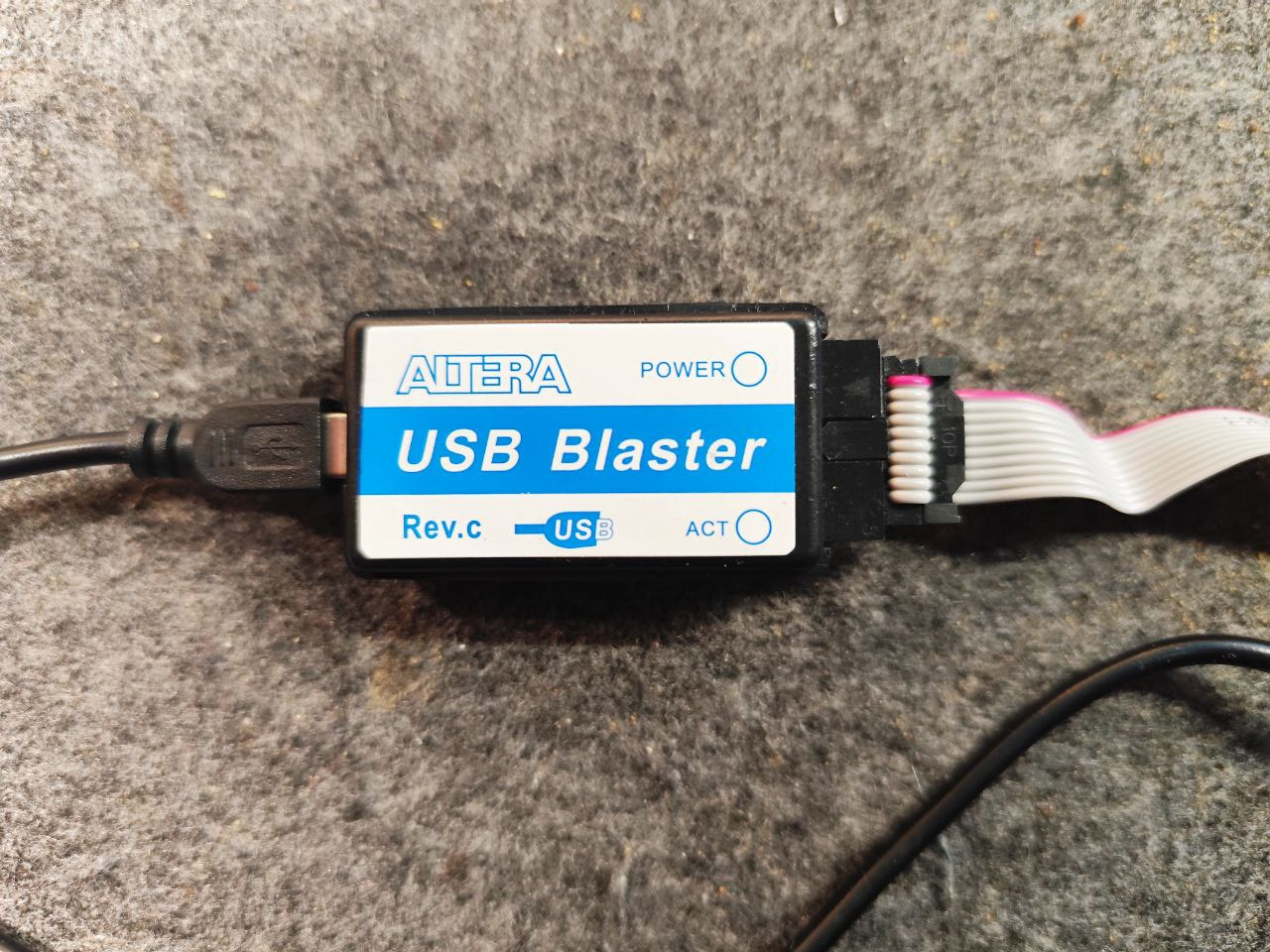
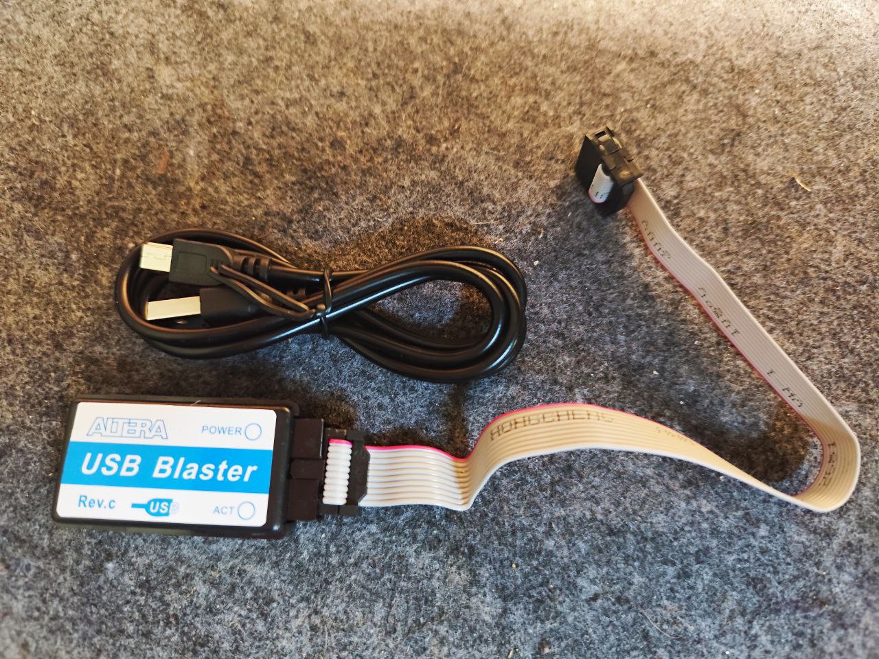
    At the same time, if I’d bought the 10-wire ribbon cable on its own, it would have cost me more than 2€. I don’t have the motivation to open it up and see what’s inside. But it’s definitely better to go for another model…

  • 64 TAPS RNS FIR

    Bertrand Selva11/10/2025 at 16:34 0 comments

    I’ve uploaded the new version of the RNS-based FIR filter, now extended to 64 TAPS (see PROGRAMME16BITS_FIRCOMPLET64TAPS.zip in project files) .
    Everything is OK !


    FIR Coefficients 

    The implemented coefficients are:

    h_int =
    
    Columns 1 through 29
      0   0   0   0   1   1   2   2   3   3   2   1  -1  -3  -6  -9 -11 -13 -14 -13  -9  -4   4  15  27  40  54  68  81
    
    Columns 30 through 58
     91  98 102 102  98  91  81  68  54  40  27  15   4  -4  -9 -13 -14 -13 -11  -9  -6  -3  -1   1   2   3   3   2   2
    
    Columns 59 through 64
      1   1   0   0   0   0

    These coefficients come from a windowed sinc with a normalized cutoff frequency of 0.1.

    They were scaled so that the sum of all taps equals 1024 (2¹⁰), allowing normalization after CRT reconstruction by a simple 10-bit right shift, with no hardware divider required. 

    All multiplication LUTs were completely rewritten to match these coefficients. The updated code is available in lut_verilog_64TAPS.v.

    Implementation results

    Target: Cyclone IV GX EP4CGX22BF14C6
    Tool: Quartus Prime 22.1std.2 (Lite Edition)

    MetricValue
    Logic elements16 007 / 21 280 (75 %)
    Registers7 982
    Embedded multipliers0 / 80 (0 %)
    Memory bits0 / 774 144 (0 %)
    PLLs0 / 3 (0 %)
    Max frequency (Slow 1200 mV 85 °C)96.9 MHz

    This confirms that the 64-tap RNS FIR is entirely built from logic elements only, with no DSP usage : a fully LUT-based architecture.


    Next step — Now that everything works:

    Decouple the input data rate from the FPGA clock so that the 64-tap pipeline can handle inputs slower than clk without any data loss or misalignment, and simulate the full chain to verify correct behavior.

    Then move on to the hardware implementation of the FIR.

  • First Functional RNS FIR

    Bertrand Selva11/09/2025 at 17:36 0 comments

    I continued exploring FIR filtering in RNS on the Cyclone IV, in line with what was presented in the previous log. This log introduces an RNS-based FIR filter that does not rely on the FPGA’s DSP blocks, uses no conventional multipliers, and is implemented entirely with combinational logic and LUTs.

    Sizing and Initial Limits

    I started with a 128-tap FIR, as defined in the previous log.
    In that form, it did not fit in the Cyclone IV E22.

    Compilation reported around 30,000 logic elements when not exploiting coefficient symmetry for a 128-tap FIR. By taking advantage of symmetry (which is generally required for linear-phase FIR filters and is a common configuration), the logic usage drops to around 15,000 logic elements for the same filter length. Even if this does not completely saturate the device, this kind of “full logic” architecture quickly eats into the available budget, especially on a family like Cyclone IV.

    With a symmetric implementation, it should be possible to push a 128-tap FIR with 16-bit input data and an effective dynamic range of about 2³⁷. That would be very close to the practical upper bound on this FPGA.

    Minimal FIR: Validating the Pipeline

    Since I had to abandon the initially targeted filter, and in order to simplify debugging and verification, I implemented a symmetric 4-tap FIR with coefficients (1, 3, 3, 1), without exploiting symmetry internally. The goal was to preserve a general architecture that can be reused for non-symmetric filters if needed.

    In this configuration:

    • Around 2,800 logic elements are used

    • No embedded RAM, no DSP blocks, no conventional multipliers

    Simulation becomes manageable again: each pipeline stage is easier to track, and debugging is more straightforward. This makes it a useful intermediate step before moving back to longer filters. The code is provided in a ZIP file attached to the project files.

    The design works. The maximum achievable frequency is about 100 MHz.
    To validate the behavior, I injected a harmonic input over 8,192 samples, covering the full dynamic range.

    The filter output matches the expected response, confirming that the FIR operates correctly in RNS, using only pure logic (including the full pipeline: the FIR itself plus the two correction stages).

    Scaling Law

    These results show that it is possible to implement an RNS FIR on a standard FPGA with 0 RAM and 0 DSP usage. The following figure shows the (approximately linear) relationship between FIR length and logic element usage.

    From the measured points, the logic usage scales approximately as:

    LE≈220×N+2200 

    (there is likely room for improvement with a more optimized implementation, but this gives the correct order of magnitude).

    For a symmetric FIR, a reasonable target is about:

    LE≈110×N

    What RNS Really Enables on FPGA

    These results help reassess where RNS is relevant in this kind of architecture. RNS is not meant to replace binary arithmetic, but it is a useful tool in the FPGA designer’s toolbox, with clear advantages in specific contexts.

    On an FPGA like the Cyclone IV E22

    Even with hardware multipliers available, a fully parallel FIR quickly runs into constraints related to accumulation, routing, pipelining, and overall logic usage. The limitation does not come only from the number of multipliers, but also from all the surrounding logic: adders, registers, fan-out, and dataflow control.

    For example, the EP4CE22 provides 66 DSP blocks with 18×18 multipliers (suitable for 16-bit inputs). This is enough to parallelize a binary FIR up to about 64 taps; that is roughly the practical upper bound for a fully parallel implementation. Even in that configuration, the logic elements are still used: they are required to build the adder tree that sums all multiplier outputs.

    It is noteworthy that, on the EP4CE22, both approaches, binary with DSPs and RNS with pure logic, end up constrained to FIR filters of about 64 taps,...

    Read more »

  • Low-pass filter design

    Bertrand Selva10/23/2025 at 17:02 0 comments

    Why Compile-Time Fixed Coefficients and "mul-by-const mod m" LUTs?

    My objective is to design the FIR without multipliers, using few wires, only shifts + additions/subtractions and ROM. Just as in the first part of the program, with the binary/RNS conversion.

    In RNS, the multiplication
    (x × h) mod m
    with h a fixed coefficient (filter tap) becomes a simple ROM lookup:

    
    LUT_m[r] = (c * r) mod m
    with c = h_int mod m,   r in [0, m-1]
    

    The first case investigated was with free coefficients (no fixed coefficient).
    With moduli:
    {7, 11, 13, 15, 17, 19, 23, 29, 31},
    and max size m=31, encoding requires 5 bits.

    All possible multiplications require:

    
    Memory = N × Σ m² × 5 bits
          = N × (7² + 11² + 13² + 15² + 17² + 19² + 23² + 29² + 31²) × 5 bits
    

    Numerically:
    Σ m² = 3545

    • N = 128 ⇒ 2,268,800 bits ≈ 246 M9K (Cyclone IV)
    • N = 256 ⇒ 4,537,600 bits ≈ 493 M9K

    So it's way too heavy to be efficient and in any case completely exceeds the resources of a Cyclone IV.
    Moreover, having free filter taps would mean a much more complicated design, with a loader to load the coefficients into the filter. I'm not a fan of this idea, especially since you'd have to load the program into the FPGA before every execution.And it's a try, a prototype. Not a real product...

    The Alternative: Compile-Time Fixed Filter Coefficients

    We store only the actually needed products because the coefficients are fixed. Then:

    
    Memory = N × Σ m × 5 bits
    

    Numerically:
    Σ m = 165

    • N = 128 ⇒ 105,600 bits ≈ 11.5 M9K
    • N = 256 ⇒ 211,200 bits ≈ 22.9 M9K

    And now, this is entirely manageable and consistent with the "multiply without multiplying" approach.
    This is the option that was chosen. 


    Filter Design: Windowed-Sinc FIR, Symmetry, Quantization and Scaling

    The FIR filter implemented here is a windowed-sinc lowpass of length N = 128, using a Hamming window for side-lobe suppression. This is the classic textbook approach for FIR design when you want maximum phase linearity (symetry) and predictable cutoff.

    We start from the ideal lowpass impulse response (the sinc), center it around n_c = (N-1)/2, and apply a symmetric window.

    h_ideal[n] = 2·fc_norm · sinc(2·fc_norm·(n - n_c)) 
    h[n] = h_ideal[n] · w[n] 
    h[n] = h[n] / sum(h[n]) // DC gain normalization 

    With N even, symmetry is perfect: h[n] = h[N-1-n]. This ensures a strictly linear phase and a constant group delay of (N-1)/2 samples.

    Quantization and scaling: The entire filter is scaled by a quantization factor Q (here, Q = 1024) and all taps are rounded to integer values:

     h_int[n] = round(Q · h[n]) 

    Every result is just "off by a factor Q". This scale is recovered by dividing by Q at the output if needed.

    The following figure show the filter elements.

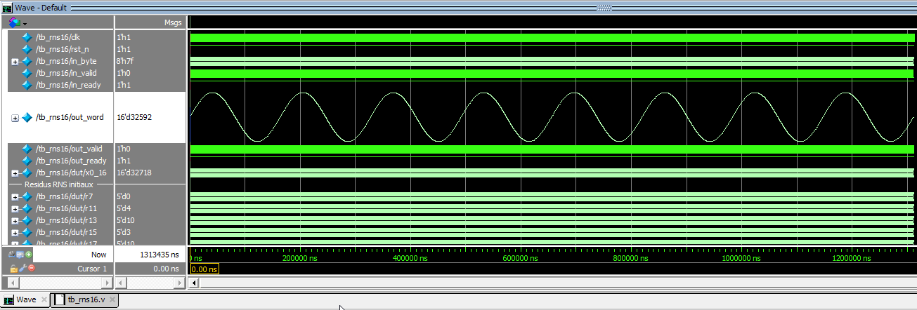
    The list of filter elements values :

      Columns 1 through 29

         0     0     0     0     0     0    -1    -1     0     0     1     1     1     0     0    -1    -1    -1    -1     1     2     2     2     1    -1    -3    -4    -3    -1

      Columns 30 through 58

         1     4     5     5     2    -2    -6    -8    -7    -3     3     8    11     9     4    -4   -12   -16   -14    -6     6 ...

    Read more »

  • Received the 16-channel logic analyzer

    Bertrand Selva10/23/2025 at 13:57 0 comments

    Another small step forward in the project: I’ve (quickly) received my 16-channel logic analyzer! The package and the box look nice.

    It will allow me to observe the behavior at the FPGA pipeline output and check the signal synchronization.

    No more hardware excuses for not moving forward…


  • Reflections on FIR Filter Architecture

    Bertrand Selva10/18/2025 at 14:53 0 comments

    I thought designing the FIR filter would be simpler -  in fact it isn’t that straightforward. To picture how data flows through the filter, I drew tables showing successive cycles with the propagation of values and the operations done at each step. The filter parameters are noted ai. The data to process are xi. Here we choose N = 4 for illustration.

    I started with a direct approach, the way you’d do it on an MCU. You’ll see it’s probably not the right method here.

    Per modulus mi, the FIR is:
    yi[n] = ( Σk=0…N−1 hi[k] · xi[n−k] ) mod mi, for all i in [1, p]

    Reconstruction by CRT:
    y[n] = CRT( y1[n], y2[n], …, yp[n] )

    To escape purely sequential thinking, it helps to reason in terms of a production line: separate “lines” manipulate data items, cycle after cycle, as in a factory.

    Moreover I count the operations and accumulations involved in an FIR with N taps and it easier to do with the following tables:

    • N−1 additions
    • N multiplications
    • N cycles of latency (here one “cycle” means the time to ingest one full sample into the FPGA. The input sample is 16-bit, the input bus is 8-bit, so it takes 2 clocks to advance one cycle.)
    • Looking at the step-5 table, we need to realize N + (N−1) + (N−2) + … + 1 = N(N+1)/2 intermediate products to fill the pipeline.
    • We need to keep N products
    • We also need to keep N−1 partial sums (accumulators)

    Step-by-step

    FIR step 1 diagram
    Figure 1. With x0 ingested, compute the four products tied to the filter {a0, a1, a2, a3}.
    FIR step 2 diagram
    Figure 2. When x1 arrives, compute its four products and start summing: x0a0 + x1a1.
    FIR step 3 diagram
    Figure 3. Ingest x2, add the new term x2a2 into the highlighted box. Start a new accumulator with x2a1 + x1a0. One more addition is still missing to complete a full convolution cycle.
    FIR step 4 diagram
    Figure 4. First full cycle completed: we can extract the first valid output.
    FIR step 5 diagram
    Figure 5. Continue the process. Values like x1a1, x1a2, x1a3, x2a2, etc., are not kept. A red boundary in the step-5 table marks what must be stored vs. what can be discarded.

    This is the direct approach. Of course, you must replicate that whole pipeline for each modulus. With k moduli, you duplicate it k times — that’s exactly where RNS parallelism comes from.

    From the direct form to parallel and transposed architectures

    While analyzing the cycle-by-cycle behavior of the direct form through these tables, a structural issue appears: for an FIR of N taps, the pipeline must effectively include N differentiated phases. At each cycle, every coefficient must be paired with its corresponding delayed sample — which requires a time-varying addressing scheme within the delay line.

    As a result, the pipeline is not stationary: its internal data paths evolve from one cycle to the next (with a global sequence of N cycles). This makes programmation and sequencing heavier.

    In addition to this non-stationary addressing, the addition chain itself must be broken into multiple intermediate stages to meet timing constraints. Together, these factors make the pipeline hard to program and tune.

    Hence the natural question: isn’t there a more regular structure, where each pipeline stage would perform exactly the same operation at every instant?

    Parallel direct form (fully parallel direct FIR)

    If one wants a “hard” (stationary) pipeline, the solution is to let the samples slide through a delay line:
    X₃ ← X₂ ← X₁ ← X₀ ← x[n].

    The multipliers always see the correct positions (x[n], x[n−1], x[n−2], …): no more dynamic addressing.

    That’s much better — but there’s still a hard point:

    • the reduction of N products (modular addition tree) must itself be pipelined;
    • otherwise, the final addition becomes heavy and limits fmax.

    Pipelining this reduction introduces a few extra cycles of latency. In practice, if one addition combines two values, the reduction tree has log₂(N) stages. ...

    Read more »

  • From 8-bit Demo to Full RNS Pipeline: +2 Across 2^37 Dynamic Range

    Bertrand Selva10/17/2025 at 09:42 0 comments

    This marks one of the key milestones towards the final objective: a design that performs +2, but this time using all 9 moduli, allowing for a dynamic range of 237.

    Input data arrives via an 8-bit bus, in two cycles per word, while output data is mapped to 16 pins.
    You can find the program on my github : https://github.com/Bertrand-selvasystems/rns-pipeline-16bit

    Program Details (What Changed)

    Data Capture, Phase 1

    Input data enters the FPGA over an 8-bit bus. On each cycle, we alternately load the low and high bytes: the first byte received (LSB) is stored temporarily, then the next one (MSB) completes the 16-bit word. As soon as the word is complete, a one-cycle validity pulse (v0) is issued to signal "word ready" for the next pipeline phase.
    This simple handshake (in_fire = in_valid & in_ready, with in_ready = rst_n) ensures the input is always ready (except during reset), simplifying both testbenches and real use.

    // Phase 1 — Capture 16b from 8b bus (LSB then MSB)
    reg  [7:0]  x_lo;
    reg         have_lo;     // 1 = LSB already captured
    reg         v0;          // 1-cycle pulse: 16b word ready
    reg  [15:0] x0_16;
    
    wire in_fire = in_valid & in_ready;
    assign in_ready = rst_n;
    
    always @(posedge clk) begin
      if (!rst_n) begin
        have_lo <= 1'b0;
        v0      <= 1'b0;
        x_lo    <= 8'd0;
        x0_16   <= 16'd0;
      end else begin
        v0 <= 1'b0; // default: no pulse
        if (in_fire) begin
          if (!have_lo) begin
            // First byte: LSB
            x_lo    <= in_byte;
            have_lo <= 1'b1;
          end else begin
            // Second byte: MSB -> complete word + v0 pulse
            x0_16   <= {in_byte, x_lo};
            have_lo <= 1'b0;
            v0      <= 1'b1; // **1-cycle pulse**
          end
        end
      end
    end
    

    On each cycle when in_fire is true:

    • If have_lo is 0, we capture the LSB.
    • If have_lo is 1, we capture the MSB, assemble the 16-bit word, and issue v0.

    This mechanism guarantees no data is lost, and every incoming byte is processed at the rate dictated by the bus and module availability.

    If you later want to handle discontinuous or asynchronous sources, simply make in_ready dependent on an actual FIFO or on the real buffering capacity of the module.

    In short: two input bytes come in, one 16-bit word goes out, marked by v0 for pipeline synchronization.

    Variable roles:
    x_lo: temporary register for the first received byte (LSB).
    have_lo: flag (1 bit) indicating whether the LSB has already been captured, controlling alternation between LSB storage and word assembly.
    x0_16: register assembling the complete 16-bit word from the newly received MSB and the stored LSB.
    v0: 1-cycle validity pulse; signals that x0_16 now holds a valid word ready for downstream processing.
    in_fire: combinational signal that indicates a data transfer is happening this cycle (in_valid & in_ready).
    in_ready: input availability signal; here, always 1 (except during reset), meaning the module never stalls the input—this is ideal for bench testing.

    Principle: On each in_fire, if no LSB is present, we store the LSB in x_lo and set have_lo to 1.
    On the next in_fire, the MSB is received, we assemble the 16-bit word into x0_16, reset have_lo to 0, and v0 emits a one-cycle pulse to signal "word ready".
    This ensures lossless, overlap-free reconstruction, and maintains correct synchronization with the downstream pipeline.

    RNS to Binary Conversion, Phase 4

    Here, we work with 9 coprime moduli (7, 11, 13, 15, 17, 19, 23, 29, 31), yielding a 37-bit dynamic range (M = 100,280,245,065). Reconstruction using the Chinese Remainder Theorem (CRT) is performed through weighted accumulation: each residue (ri) is assigned a value read from a precomputed ROM table (T), and these terms are summed in multiple pipeline stages, each with a reduction modulo M.

    // Phase 4 — Pipelined CRT "mod M" at each addition stage
    localparam [36:0] M = 37'd100280245065;
    
    // Modular addition: returns (a+b) mod M
    function [36:0] add_modM;
      input [36:0] a, b;
      reg   [37:0] s;   // 0..(2*M-2) < 2^38
    begin
      s = {1'b0,a} + {1'b0,b};
      if (s >= {1'b0,M}) s = s - {1'b0,M};
      add_modM = s[36:0];
    end
    endfunction
    ...
    Read more »

  • Automatic Generation of RNS LUTs in MATLAB

    Bertrand Selva10/16/2025 at 09:02 0 comments

    This MATLAB/Octave script automatically computes look-up tables (LUTs) for a Residue Number System (RNS) with a given set of moduli. It generates:

    • The total product M = m1 * m2 * ... * mn
    • The reconstruction coefficients Ai
    • An example table Tj for a modulus mj
    • Verilog-style outputs (case / endcase) ready to integrate into your FPGA design

    Method

    The reconstruction follows the classical Chinese Remainder Theorem (CRT):

    M  = product of all moduli
    Mi = M / mi
    Ai = (Mi * inverse(Mi mod mi, mi)) mod M
    Tm(r) = (Ai * r) mod M   for r = 0 .. mi-1
    

    Each Tm table stores precomputed modular residues, allowing fast RNS operations on FPGA without any division or modulo logic.

    MATLAB/OCTAVE Script

    close all;
    clear all;
    clc;
    format long g;
    
    %% RNS LUT generation
    
    %% Moduli list
    moduli = [7 11 13 15 17 19 23 29 31];
    
    %% Compute M
    M = 1;
    for i = 1:length(moduli)
        M = M * moduli(i);
    end
    disp(M);   % 100280245065
    
    %% Coefficients Ai
    Ai = zeros(1, numel(moduli));   % preallocation
    for i = 1:numel(moduli)
        m  = moduli(i);
        Mi = M / m;                 % M_i
        t  = mod(Mi, m);            % (M_i mod m)
        [g, x, ~] = gcd(t, m);      % t*x + m*y = g
        if g ~= 1
            error('No modular inverse for m=%d (gcd=%d).', m, g);
        end
        inv_t = mod(x, m);          % inverse of t modulo m
        Ai(i) = mod(inv_t * Mi, M); % A_i = (M_i * inv_t) mod M
    end
    
    %% Example LUT Tj (e.g., j=9 -> m = 31)
    j  = 9;                         % choose index in 'moduli'
    mj = moduli(j);
    Tj = zeros(1, mj);              % Tj(r+1) = (Ai(j)*r) mod M
    
    for r = 0 : mj-1
        Tj(r+1) = mod(Ai(j) * r, M);
    end
    
    % Display
    disp('Ai ='); disp(Ai);
    disp(['T' num2str(mj) '(r) for r=0..' num2str(mj-1) ':']);
    disp(Tj);
    
    %% Verilog-like table generator
    for j = 1:numel(moduli)
        m = moduli(j);
        fprintf('function [36:0] T%d;\n', m);
        fprintf('  input [4:0] r;\n  begin\n    case (r)\n');
        for r = 0:m-1
            fprintf('      5''d%-2d : T%d = 37''d%u;\n', r, m, mod(Ai(j)*r,M));
        end
        fprintf('      default: T%d = 37''d0;\n    endcase\n  end\nendfunction\n\n', m);
    end
    

    Notes

    • Chosen moduli: [7, 11, 13, 15, 17, 19, 23, 29, 31]
    • Total product: M = 100,280,245,065
    • Because 2^37 = 137,438,953,472 > M, 37-bit wide signals are sufficient.
    • Each input r fits in 5 bits (max modulus = 31).
    • In this configuration, M is large enough to prevent overflow when using Q15 coefficients in an RNS-based FIR filter (the goal project).

    Conclusion

    This log automates the generation of RNS LUTs and Verilog snippets. Run the script, copy the output, and integrate it directly into your FPGA design without manual editing. Because Typing 300 Constants by Hand Is for Humans...

    Results

    function [36:0] T7;
      input [4:0] r;
      begin
        case (r)
          5'd0  : T7 = 37'd0;
          5'd1  : T7 = 37'd28651498590;
          5'd2  : T7 = 37'd57302997180;
          5'd3  : T7 = 37'd85954495770;
          5'd4  : T7 = 37'd14325749295;
          5'd5  : T7 = 37'd42977247885;
          5'd6  : T7 = 37'd71628746475;
          default: T7 = 37'd0;
        endcase
      end
    endfunction

    function [36:0] T11;
      input [4:0] r;
      begin
        case (r)
          5'd0  : T11 = 37'd0;
          5'd1  : T11 = 37'd91163859150;
          5'd2  : T11 = 37'd82047473235;
          5'd3  : T11 = 37'd72931087320;
          5'd4  : T11 = 37'd63814701405;
          5'd5  : T11 = 37'd54698315490;
          5'd6  : T11 = 37'd45581929575;
          5'd7  : T11 = 37'd36465543660;
          5'd8  : T11 = 37'd27349157745;
          5'd9  : T11 = 37'd18232771830;
          5'd10 : T11 = 37'd9116385915;
          default: T11 = 37'd0;
        endcase
      end
    endfunction

    function [36:0] T13;
      input [4:0] r;
      begin
        case (r)
          5'd0  : T13 = 37'd0;
          5'd1  : T13 = 37'd53997055035;
       ...

    Read more »

  • Receiving the USB Blaster

    Bertrand Selva10/14/2025 at 14:17 0 comments

    I just received the Altera USB Blaster, used to program the Cyclone IV FPGA.

    What it’s for:

    • JTAG interface between the PC and Intel/Altera FPGA or CPLD (Cyclone, MAX, etc.)

    • Programming of configuration files (.sof, .pof, .jic) via Quartus

    • Hardware debugging access (SignalTap, JTAG UART, boundary-scan)

    • Low-level memory read/write and diagnostic operations

    The real tests will begin soon. I’ll post a log once the first successful programming sequence is done.

View all 12 project logs

Enjoy this project?

Share

Discussions

Bertrand Selva wrote 12/06/2025 at 10:01 point

The video is excellent (the kind of professor one wishes they had).
I hadn’t seen that lecture before starting my own RNS project, and it would clearly have helped me structure things much earlier.

I’ve just commented on his video in the hope of opening a small technical discussion.
Thank you again for sharing these materials.

  Are you sure? yes | no

Pascal wrote 12/05/2025 at 08:55 point

I found some interesting resources regarding RNS, which you might enjoy as well. There is a book on Computer Arithmetic which has a whole chapter dedicated to RNS: https://web.ece.ucsb.edu/~parhami/text_comp_arit.htm 

Buying the book is a little bit costly but a bit of google-foo solves this nicely. The same professor also has his presentation online on Youtube regarding this chapter: https://www.youtube.com/watch?v=aPagJWEeDMc

  Are you sure? yes | no

Does this project spark your interest?

Become a member to follow this project and never miss any updates