Ken Yap
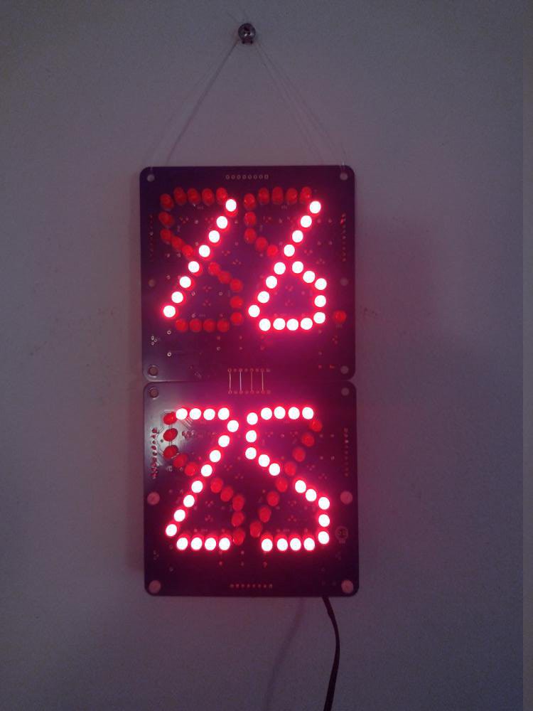
Vertical display
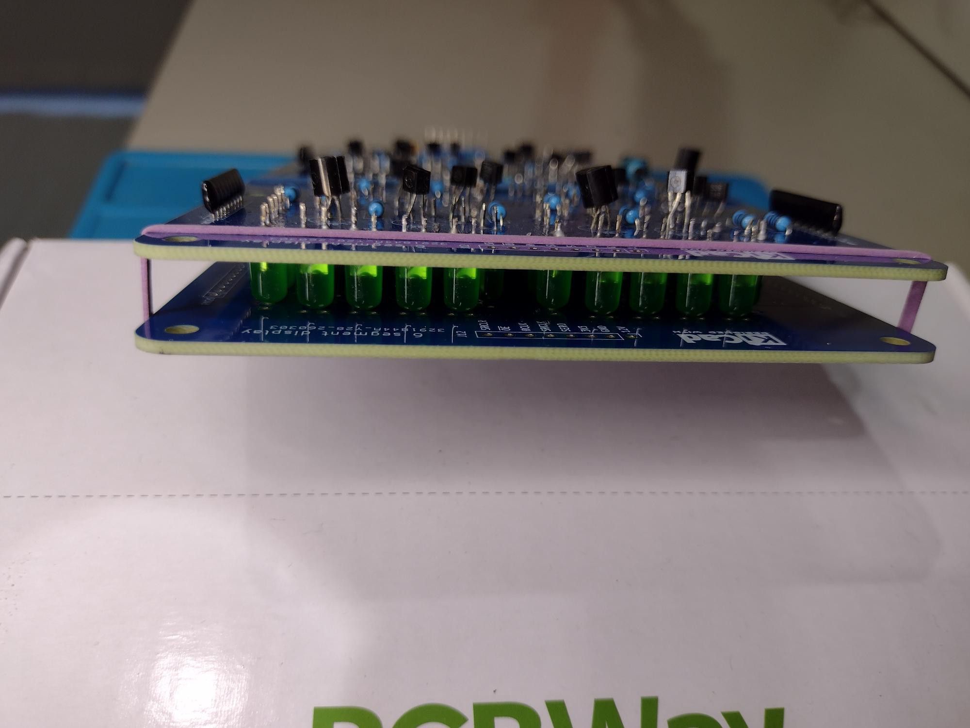
This is the latest iteration of displays that use discrete domed LEDs to form segments developed for #6 segments suffice and implemented in #6 segment 2 digit LED display board and #7 segment 2 digit LED display board as well as other side projects such as #Ancient PMOS technology clock and #Ancient 12 hour display. But the time has come to declare a new project as several design decisions have been made for this series of displays.
- Vertical stacking versus horizontal stacking. Horizontal stacking seems natural to make multiples of 2 digits. However while looking in a shop window in Llanes, I saw a consumer LED clock where the digits were stacked vertically. I also realised that the clock on my smartphone lock screen also stacks vertically. Several advantages accrue:
No separator between hours and minutes (and seconds, if present) is needed. The traditional blinking colon can be changed to a less prominent flashing dot.
Portrait format instead of landscape which makes it easier to hang on walls. The MCU board can be attached to the bottom board providing some weight to keep the stack orthogonal.
The display could be used to display say temperature and humidity without confusion from horizontal stacking.
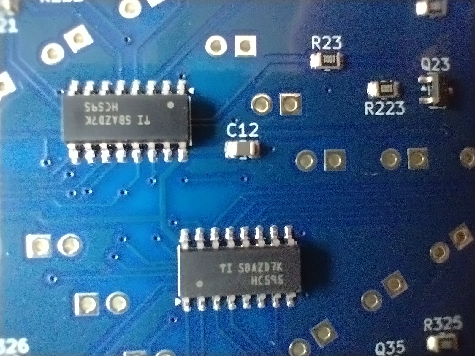
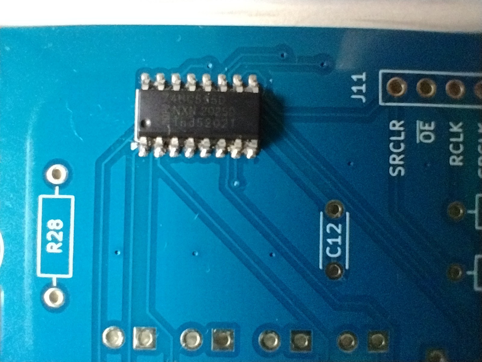
Chained shift registers with static drive for each segment versus segment-digit multiplexed display. The latter requires less components: a set of segment drivers and a set of digit drivers, whereas the former requires more drivers, one for each segment. Also a multiplexed scheme requires more MCU output pins and firmware support whereas a shift register chain only requires 3 lines minimum and 1 more if PWM dimming is implemented. Static drive also allows increasing the height of the stack with no change in lines, only chaining. If I use LED filaments later multiplexing becomes harder as the current per segment is around 30 mA so a fully lit digit would draw 210 mA divided by the per digit duty cycle, requiring more care with board tracks.
Constant current LED drive. The 6 segment font has 4 or 5 LEDs per segment in the same display whereas it's fixed at 3 or 4 for all segments in the 7 segment font. This either requires different limiting resistors for the segments, which introduces a dependency on the supply voltage and the voltage drop of the LEDs which depends on the colour (junction type). This becomes even more important for LED filaments which I hope to use as segments in a future design. For this reason I have chosen to implement constant current drive. In a previous iteration I used the TL431 to generate a bias rail for the drivers. Then it occurred to me that there already is a reference rail, the 3.3 V supply for the MCU. (This is also a good opportunity to transition to 3.3 V MCUs as the 5 V MCUs are getting fewer.) Granted this is bit high and results in wasting about 2.5V across the limiting resistor. But I have elected to use boost converters to provide the LED power which provide flexibility.
Surface mount versus through hole technology. More transistors and resistors in the static drive method push the design towards SMT where the parts are cheaper and more can be packed on the board. It also allows automated assembly for those who want to avoid soldering lots of small parts.
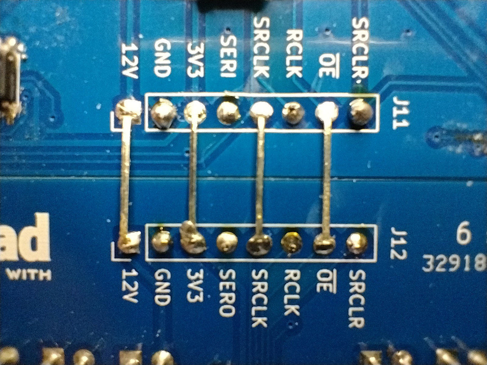
Eliminate flying wires. The connector on the display board is designed to plug into an 8 pin Dupont pin socket on the MCU drive board, no other connections are required.
Use a boost converter to provide the LED power. I used to worry about the voltage provided by wall warts, usually 5V or 12V and this was reflected in the design that resulted. Now a wide range of wall wart voltages is accepted as the LED supply voltage can be adjusted by trimpot, and a small SMD LDO regulator provides a calm 3.3 V rail for the MCU, which does not need much current.
First prototype
I made a prototype with the vertical design and it looked like this. Straight away I realised that the proportion was wrong, the digit...
Read more »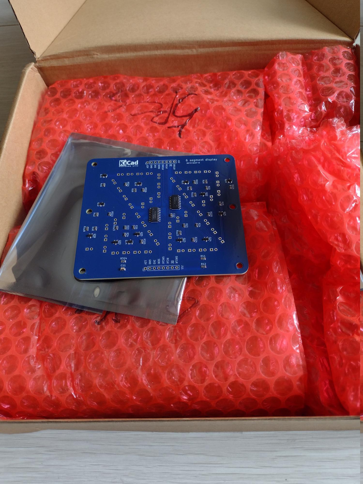

 Yann Guidon / YGDES
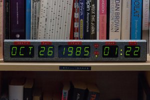
 Stephen Holdaway