Ken Yap
-
An assessment of the assembled boards
5 hours ago • 0 comments![]()
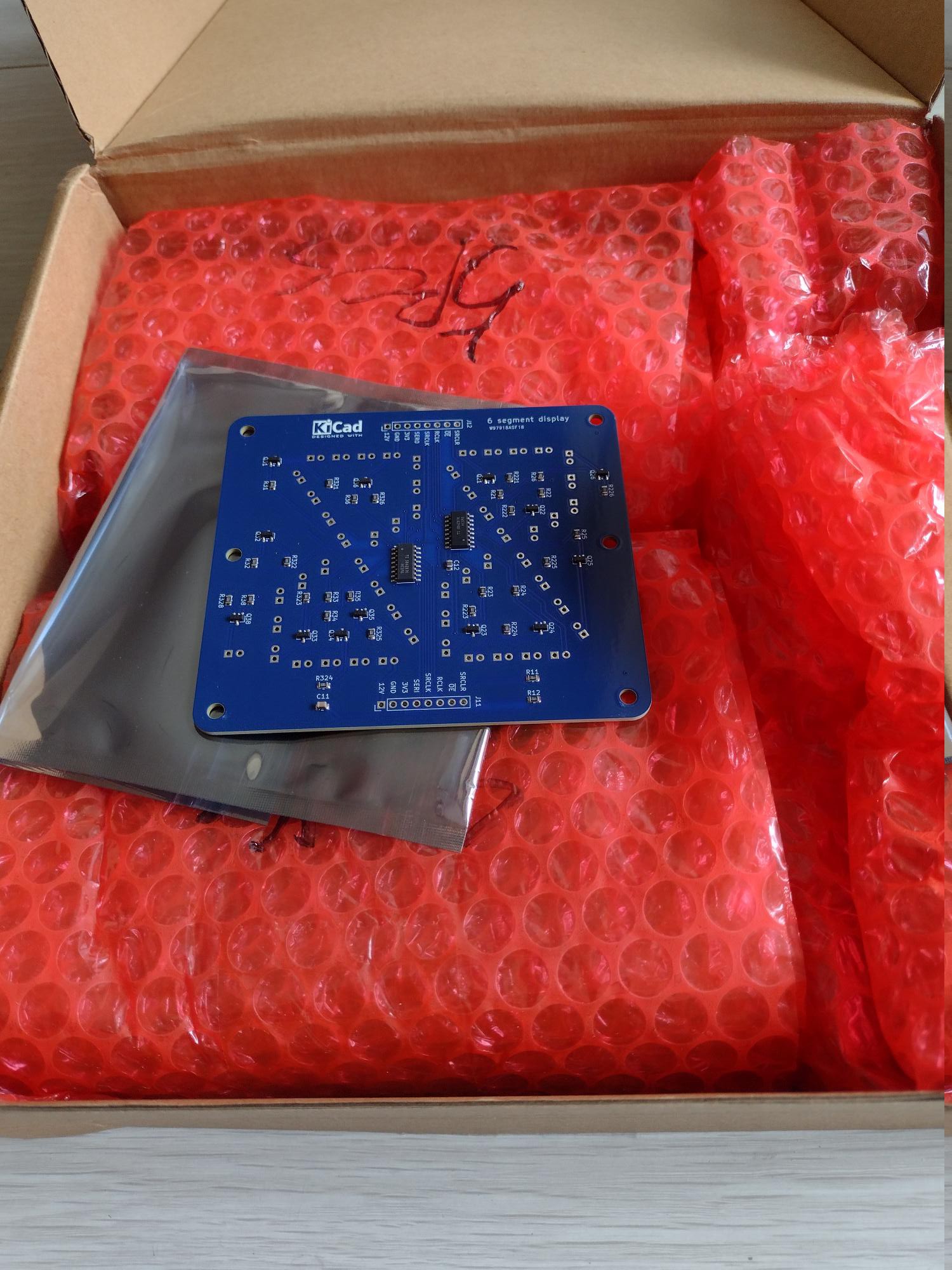
The assembled boards have arrived from PCBWay, wrapped extremely well in plastic bubble and each board in a reusable anti-static bag. I was half expecting a stack of boards, but of course that's wrong as the boards have SMD components mounted.
![]()
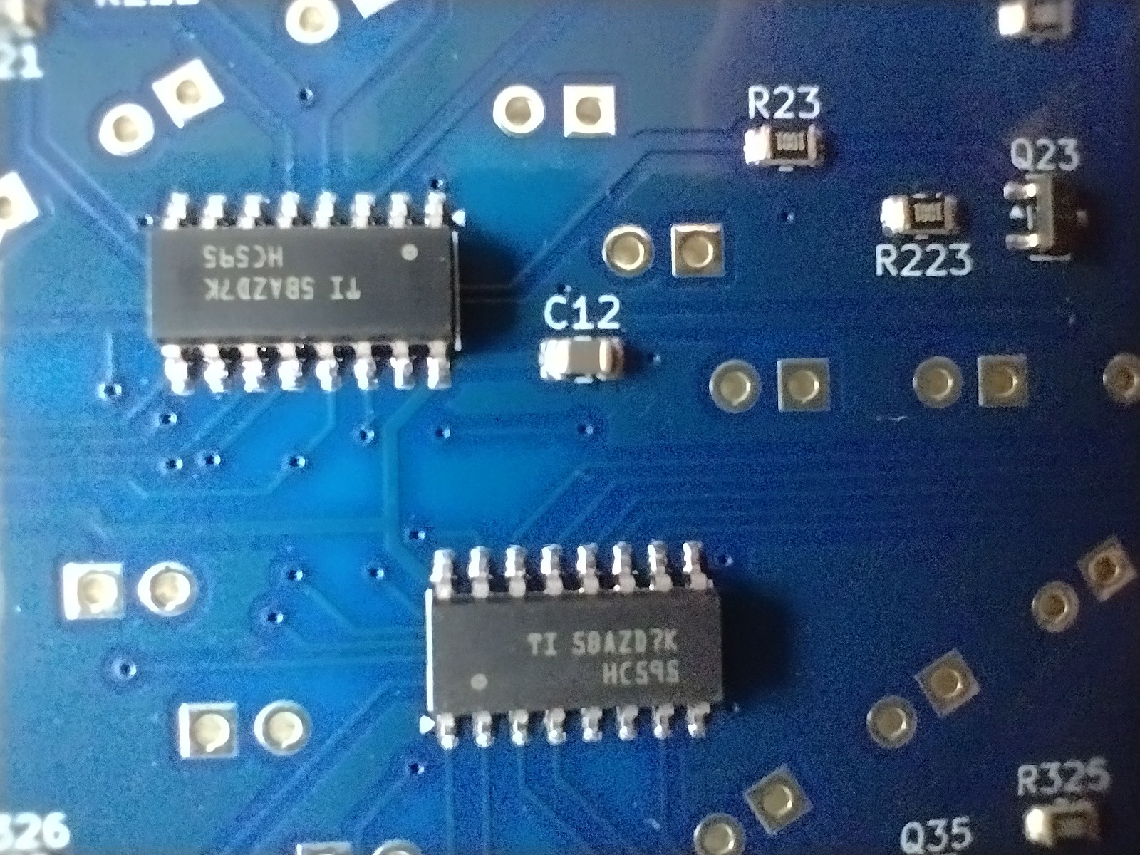
The quality as you can see is impeccable. They sent me a picture of the first board to confirm that the placement of the parts was correct. It was a photo of a real board because the SS8050 SMD transistors had the marking Y1, the short code for this part.
![]()
Naturally my manual but adequate soldering shown above is no match for reflow soldering. The pictures also show that I'm not really set up to take good macro photos, there is reflection from the shiny solder. Maybe I need one of those digital microscopes.
So what were the durations and costs? Bear in mind that this will vary widely with project.
- Day 0: The order was placed and PCB fabrication started on May 19.
- Day 3: The boards were completed on May 22.
- Day 9: The required parts were collected by May 28.
- Day 15: Board assembly boards was completed and they were shipped on June 3. Interesting that the estimated build time was 25-30 days, perhaps for leeway for complex boards or hard to source parts. This project only requires 2 copper layers and widely available parts.
- Day 23: I had opted for cheap Global Express shipping so the boards arrived June 11. Note that the local handling (customs, last km courier) took a few days, so it's not just transport time from China.
As for the costs, the boards are under 100x100 mm so each of 10 boards is $0.50. Parts were $0.71 and assembly was $2.90 resulting in $4.11 per board. Naturally this is highly dependent on the parts and the complexity of the board. You have to decide if it's worth paying for professional assembly. A factor is whether you are a hobbyist or a commercial firm. If you are in a hurry because it's a commercial project, then the cost shoots up for rush jobs. If there are several iterations then the cost multiplies. Then again, manual assembly is more prone to errors, and you have to clean off soldering residue.
So now to populate the boards with 5 mm LEDs, stitch two together and get a display working. By the way if you are building displays out of discrete LEDs like me, eschew 3 mm LEDs and go for 5 mm LEDs. Not only do they look more attractive, like glowing domes rather than points of light, but they are also more robust. The 3 mm LED leads break off easily if soldered more than once, after all the pin spacing is 2.54 mm. Naturally go for diffused bodies rather than clear bodies.
-
Generating PCB production files with kicad-cli
05/17/2026 at 23:31 • 2 commentsFor a couple of versions now, KiCad has had a command line tool for generating production outputs. How does this improve the workflow? For one thing, instead of specifying outputs and options, and generating files from the GUI, you do it from the command line. This allows you to use scripts which gives reproducible results, free from having to ensure that all the right boxes have been filled in or ticked in the GUI. For this project i have used a Makefile. Here it is:
PROJECT=6segment
VERSION=7
SCHFILE=$(PROJECT).kicad_sch
PCBFILE=$(PROJECT).kicad_pcb
LAYERS=F.Cu,B.Cu,F.Mask,B.Mask,F.Silkscreen,B.Silkscreen,Edge.Cuts
OUTPUTDIR=output
BOMFIELDS=$${QUANTITY},Reference,Value,Footprint,Description,Type,Manufacturer,MPN
BOMLABELS=Quantity,Designator,Value,Package,Description,Type,Manufacturer,MPN
BOMFILE=$(OUTPUTDIR)/$(PROJECT)-bom.csv
POSFILE=$(OUTPUTDIR)/$(PROJECT)-pos.csv
ZIPDIR=/var/tmp/Tmp
ZIP=$(ZIPDIR)/$(PROJECT)-v$(VERSION).zip

all:    gerbers bom pos zip

$(OUTPUTDIR):
        mkdir -p $(OUTPUTDIR)

gerbers:        $(PCBFILE) $(OUTPUTDIR)
        mkdir -p $(OUTPUTDIR)
        kicad-cli pcb export gerbers -o $(OUTPUTDIR) --no-protel-ext -l $(LAYERS) $<
        kicad-cli pcb export drill -o $(OUTPUTDIR) --excellon-separate-th $<
        kicad-cli pcb export ipcd356 -o $(OUTPUTDIR)/$(PROJECT)-netlist.ipc $<

bom:    $(SCHFILE) $(OUTPUTDIR)
        kicad-cli sch export bom -o $(BOMFILE) --fields '$(BOMFIELDS)' --labels '$(BOMLABELS)' --group-by Value --ref-range-delimiter '' $<

pos:    $(PCBFILE) $(OUTPUTDIR)
        kicad-cli pcb export pos -o $(POSFILE) --format csv --units mm --side back --use-drill-file-origin --smd-only $<
        sed -i -e '1s/Ref,Val,Package,PosX,PosY,Rot,Side/Designator,Value,Footprint,Mid X,Mid Y,Rotation,TB/' -e 's/bottom/B/' $(POSFILE)

zip:    gerbers
        rm -f $(ZIP)
        zip -jo $(ZIP) $(OUTPUTDIR)/*.{gbr,drl,ipc}
For the gerbers rule we generate the layers specified, then generate the two drill files, and finally a IPC-D-356 netlist to help the fabricator test the boards. A zip rule combines them into a file ready to upload.
The other two rules generate the Bill of Materials (BOM) and Component Placement List (CPL, also called POS) files containing assembly information. I looked at PCBWay's instructions for BOM and POS file format, and tried to follow it as close as possible.
For the BOM, the order of the labels and content of the columns is specified with the --labels and --fields arguments to the kicad-cli sch export bom command. ${QUANTITY} is a meta-field, it will be replaced with the number of items in that row. The $$ is to get a single $ past Makefile escaping rules. Here's what the BOM contains:
"Quantity","Designator","Value","Package","Description","Type","Manufacturer","MPN"
"1","C11","10u","Capacitor_SMD:C_0805_2012Metric","Unpolarized capacitor, small symbol","SMD","",""
"1","C12","100n","Capacitor_SMD:C_0805_2012Metric","Unpolarized capacitor, small symbol","SMD","",""
"13","Q21,Q22,Q23,Q24,Q25,Q26,Q31,Q32,Q33,Q34,Q35,Q36,Q38","SS8050","Package_TO_SOT_SMD:SOT-23","General Purpose NPN Transistor, 1.5A Ic, 25V Vce, SOT-23","SMD","",""
"2","R11,R12","47k","Resistor_SMD:R_0805_2012Metric","Resistor, small symbol","SMD","",""
"26","R21,R22,R23,R24,R25,R26,R31,R32,R33,R34,R35,R36,R38,R221,R222,R223,R224,R225,R226,R321,R322,R323,R324,R325,R326,R328","1k","Resistor_SMD:R_0805_2012Metric","Resistor, small symbol","SMD","",""
"2","U1,U2","74HC595D","Package_SO:SOIC-16_3.9x9.9mm_P1.27mm","8-bit serial in/out Shift Register 3-State Outputs","SMD","",""
The Type field is an additional attribute that was added to each symbol to be assembled and is always SMD, as the assembly of the THT LEDs and the Dupont pin header will be done by me. The Manufacturer and MPN fields were left blank (actually kicad-cli will generate blank content for non-existent attributes) so that PCBWay can do the sourcing of the parts. Like nearly all other PCBA companies in China, PCBWay is not a stockist and will look on the market for the parts you specified. A couple of the tickboxes in the order form asks if you are willing to use equivalent or made in China parts. I have absolutely no issues with equivalent parts or made in China parts, as this project uses commodity parts, and they are probably made in China anyway.
I worried a bit about the order of the columns and tried to follow the PCBWay guidelines. In the end it wasn't a problem, as they understood what I wanted and anyway the confirmation CSV came back in a different order. The only queries were whether I accepted the manufacturer of the SS8050 jelly-bean transistors, and changing the 74HC595D to 74HC595DR because SOIC by itself is not sufficiently specific and you must specify the correct package for the appropriate dimensions and pin pitch.
(Here I want to put in a plug for the SS8050 which seems to have originated with Fairchild decades ago in the TO-92 package. I think it's a superior jelly-bean transistor to the commonly used MMBT3904 as it has excellent gain characteristics across the range of current and high current capacity. One drawback is the relatively low Vceo of 25V.)
Now the POS file specifies the positions of the centroid of the SMD parts for the pick and place machine. Unfortunately kicad-cli doesn't allow a custom order for the columns. However I had a sed command to change the labels on the columns to close to the PCBWay example and also change the assembly side of "bottom" to B.
Designator,Value,Footprint,Mid X,Mid Y,Rotation,TB
"C11","10u","C_0805_2012Metric",71.120000,15.240000,0.000000,B
"C12","100n","C_0805_2012Metric",43.180000,50.800000,-90.000000,B
"Q21","SS8050","SOT-23",33.020000,76.200000,90.000000,B
"Q22","SS8050","SOT-23",22.860000,66.040000,-90.000000,B
"Q23","SS8050","SOT-23",38.100000,33.020000,-90.000000,B
"Q24","SS8050","SOT-23",22.860000,33.020000,-90.000000,B
"Q25","SS8050","SOT-23",12.700000,50.800000,-90.000000,B
"Q26","SS8050","SOT-23",5.080000,76.200000,90.000000,B
"Q31","SS8050","SOT-23",86.360000,83.820000,90.000000,B
"Q32","SS8050","SOT-23",86.360000,60.960000,90.000000,B
"Q33","SS8050","SOT-23",76.200000,33.020000,-90.000000,B
"Q34","SS8050","SOT-23",67.630000,33.020000,90.000000,B
"Q35","SS8050","SOT-23",63.500000,38.100000,-90.000000,B
"Q36","SS8050","SOT-23",63.500000,76.200000,90.000000,B
"Q38","SS8050","SOT-23",91.440000,38.100000,-90.000000,B
"R11","47k","R_0805_2012Metric",25.400000,20.320000,180.000000,B
"R12","47k","R_0805_2012Metric",25.400000,15.240000,180.000000,B
"R21","1k","R_0805_2012Metric",30.480000,71.120000,90.000000,B
"R22","1k","R_0805_2012Metric",20.320000,71.120000,-90.000000,B
"R23","1k","R_0805_2012Metric",35.560000,43.180000,-90.000000,B
"R24","1k","R_0805_2012Metric",27.940000,43.180000,-90.000000,B
"R25","1k","R_0805_2012Metric",12.700000,58.420000,-90.000000,B
"R26","1k","R_0805_2012Metric",20.320000,76.200000,90.000000,B
"R31","1k","R_0805_2012Metric",86.360000,76.200000,90.000000,B
"R32","1k","R_0805_2012Metric",88.900000,53.340000,90.000000,B
"R33","1k","R_0805_2012Metric",71.120000,43.180000,-90.000000,B
"R34","1k","R_0805_2012Metric",71.120000,38.100000,-90.000000,B
"R35","1k","R_0805_2012Metric",66.040000,43.180000,-90.000000,B
"R36","1k","R_0805_2012Metric",66.040000,71.120000,90.000000,B
"R38","1k","R_0805_2012Metric",88.900000,43.180000,90.000000,B
"R221","1k","R_0805_2012Metric",27.940000,76.200000,-90.000000,B
"R222","1k","R_0805_2012Metric",27.940000,66.040000,90.000000,B
"R223","1k","R_0805_2012Metric",38.100000,38.100000,90.000000,B
"R224","1k","R_0805_2012Metric",30.480000,33.020000,-90.000000,B
"R225","1k","R_0805_2012Metric",20.320000,50.800000,-90.000000,B
"R226","1k","R_0805_2012Metric",5.080000,71.120000,-90.000000,B
"R321","1k","R_0805_2012Metric",72.390000,76.200000,-90.000000,B
"R322","1k","R_0805_2012Metric",81.280000,53.340000,-90.000000,B
"R323","1k","R_0805_2012Metric",76.200000,43.180000,90.000000,B
"R324","1k","R_0805_2012Metric",71.120000,20.320000,0.000000,B
"R325","1k","R_0805_2012Metric",60.960000,33.020000,-90.000000,B
"R326","1k","R_0805_2012Metric",60.960000,71.120000,-90.000000,B
"R328","1k","R_0805_2012Metric",93.980000,43.180000,90.000000,B
"U1","74HC595D","SOIC-16_3.9x9.9mm_P1.27mm",40.640000,60.325000,0.000000,B
"U2","74HC595D","SOIC-16_3.9x9.9mm_P1.27mm",53.340000,51.435000,180.000000,B
Again PCBWay had no problems understanding what I wanted. So now to say yes to the two changes and get approval for the sponsorship.