 Luis Mestre

This is a fairly complex project as it stands specially from the embedded system point of view. I would like to break this down for now into 3 main components: the tip, the custom PCB and the stage.
- The tip is currently a commercial AFM tip I was able to get for free from my lab to test things out. But I am working on an etching jig to make my own tips out of watch tuning forks and electro etched tungsten wire similar to the Mad City Labs AFM https://www.youtube.com/watch?v=K_k5UsHlwN4
- The custom PCB was fully designed by me and is aggressively cost optimised and will be further cost optimised again to reduce the cost further. The fully assembled price per PCB stands at something like 70ish bucks from JLCPCB. It's still a working progress as there are some things to optimise but as it stands it works fine. Software is really the magic here. I implemented a digital lock-in amplifier with its own DDS signal generator as well as PID for amplitude modulated (AM) and PLL frequency modulated (FM) AFM. Additionally, there is also Q control to dampen the tuning fork if someone wants to operate in AM mode in vacuum. The lock-in is implemented using the STM's own included peripheral ADC and DAC making this extremely cheap since the uC chip costs like 7 bucks. I actually have more than one lock-in channel as I might add closed loop control to the stage for ultimate precision.
-The stage is a fun one. For the testing stage in the pictures, I have a 3D printed flexure stage. There are 2 linear 3D printed flexure stages stacked on top of each other forming the x and y axis. The z axis is a piezo buzzer. The flexure stage is based on the work of Eric Clot who realised hepatic feedback piezos are great cheap precision actuators! His project is linked here https://hackaday.io/project/202424-haptic-piezo-for-high-precision-actuation I want to design a flexure stage and have this CNC machined by JLCPCB (Wire EDM is very expensive...). There are currently some piezo hysteresis issues I am trying to sort out (lines outside the calibration grid squares in the images) but I am looking into this so this can be close to a commercial educational system for <1/20th of the price tag.
I will try my best to document the project in detail but I am also currently doing a Physics PhD so it might take some time to get updates on here.
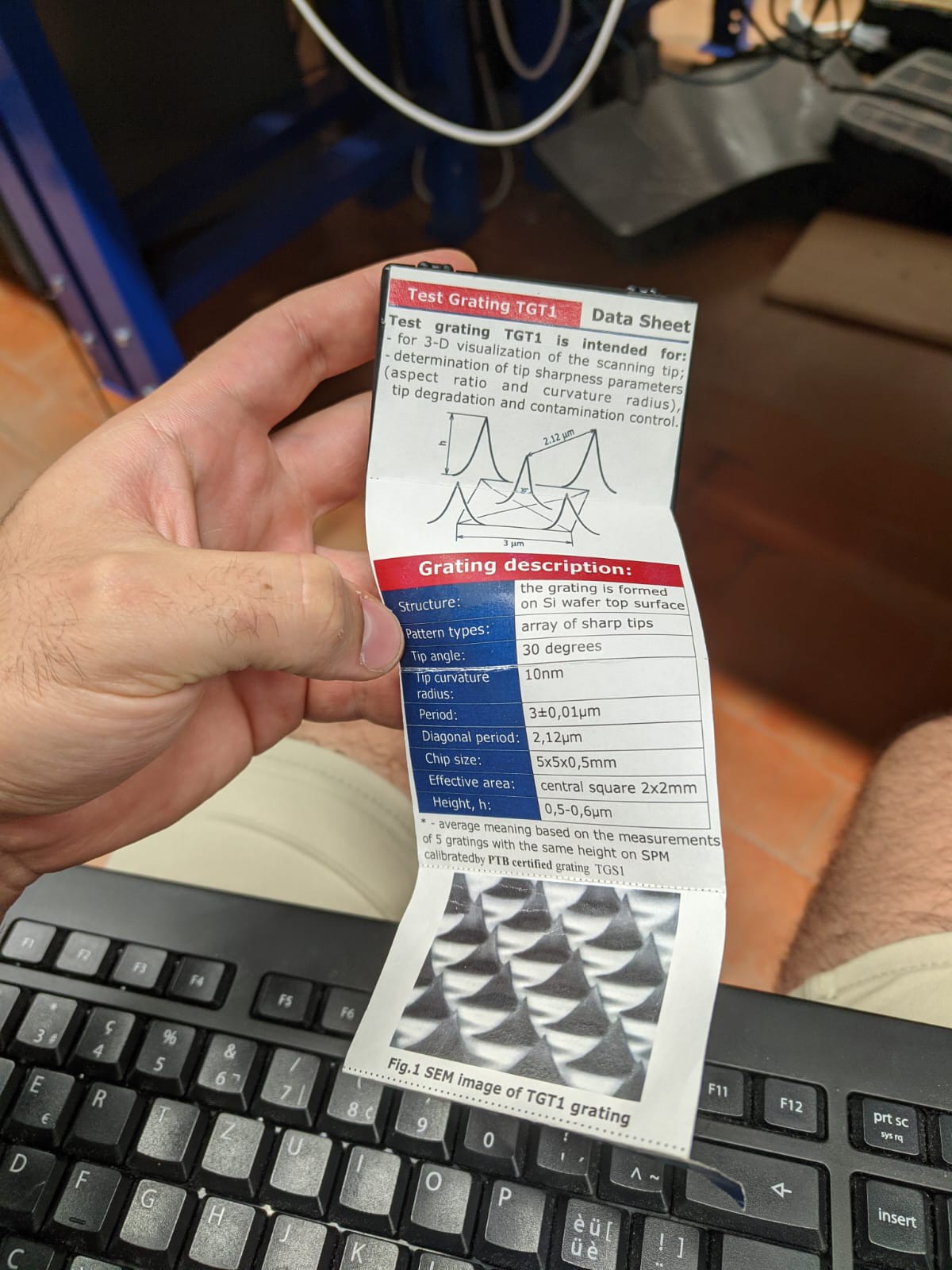
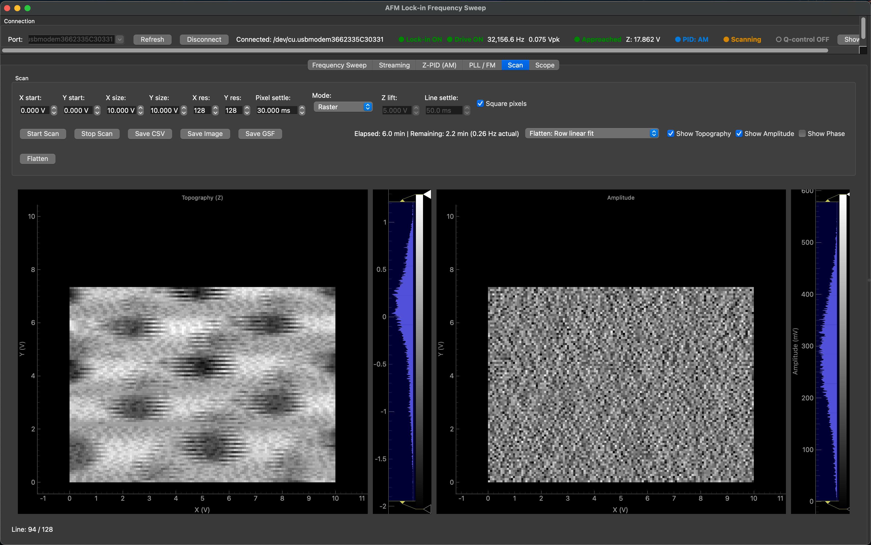
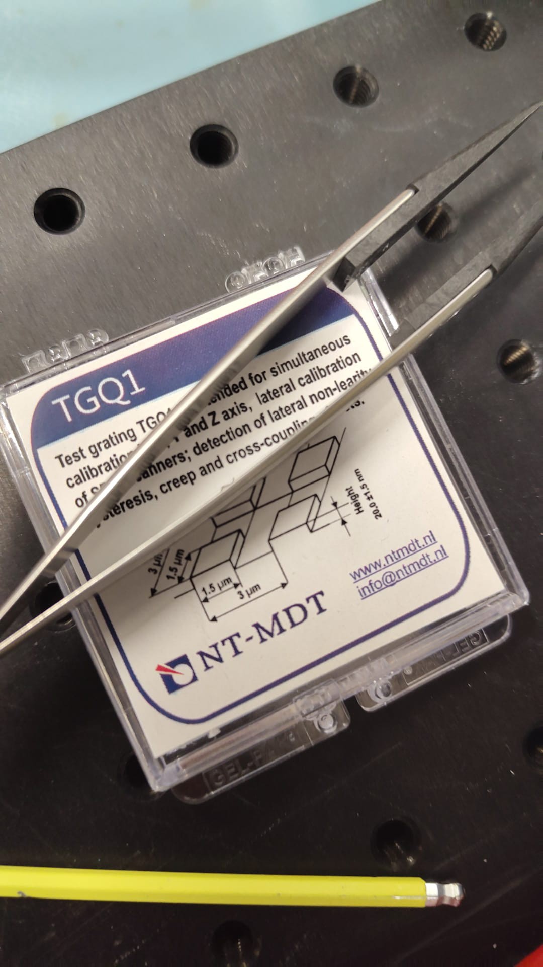 Here is an example of the 20nm step with improved noise. The previous steps looked like this:
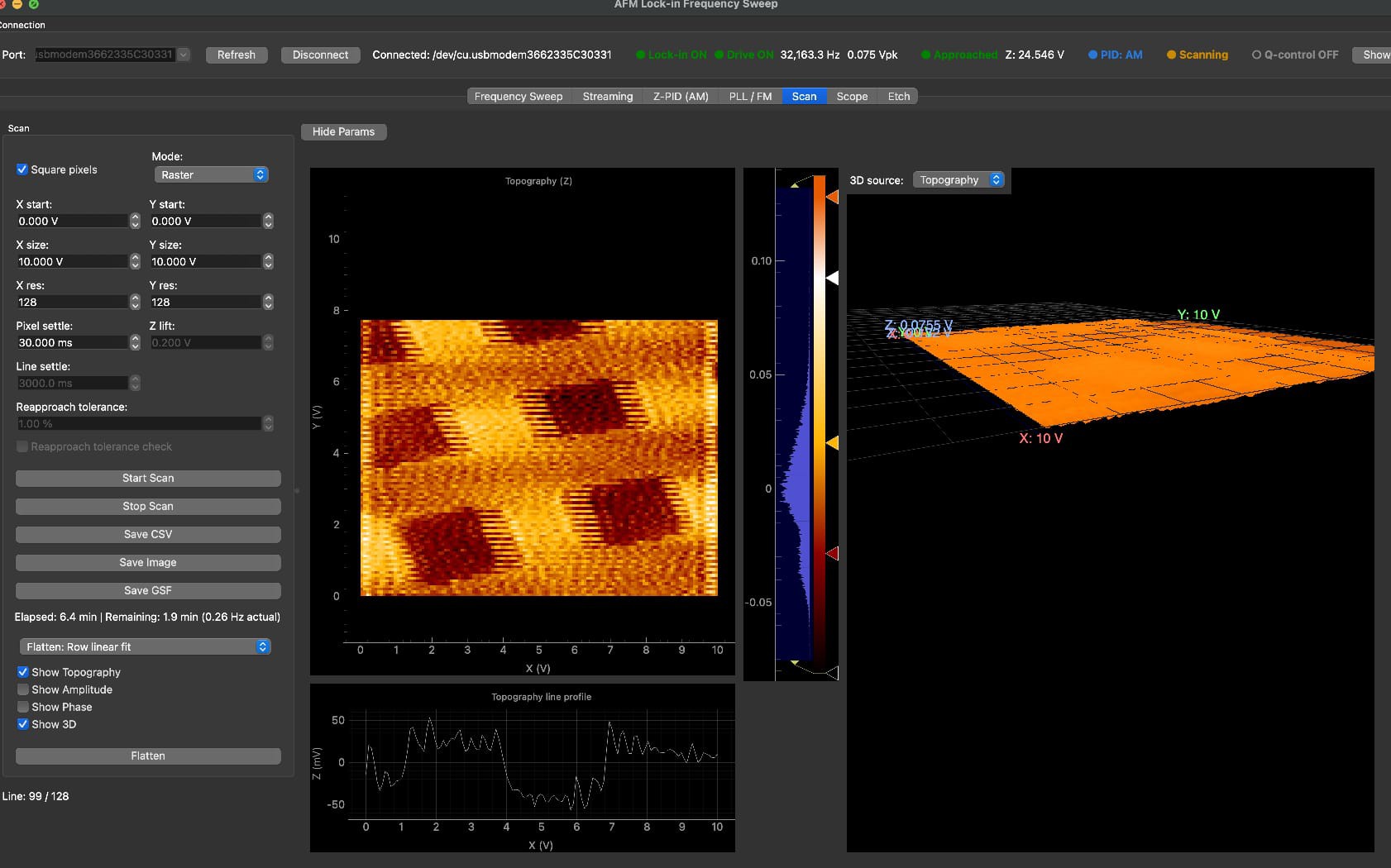 With the improved shielding on the tuning fork wires to the TIA the same 20nm step is much cleaner. I believe now I am limited by environmental vibrations due to my damping being a bike inner tube, to see atomic layers, I likely need and enclosure and the setup suspended by springs with eddy current damping from magnets similar to Dan Berard's STM. but I would say this is pretty good already for most applications like looking at cells or DNA.
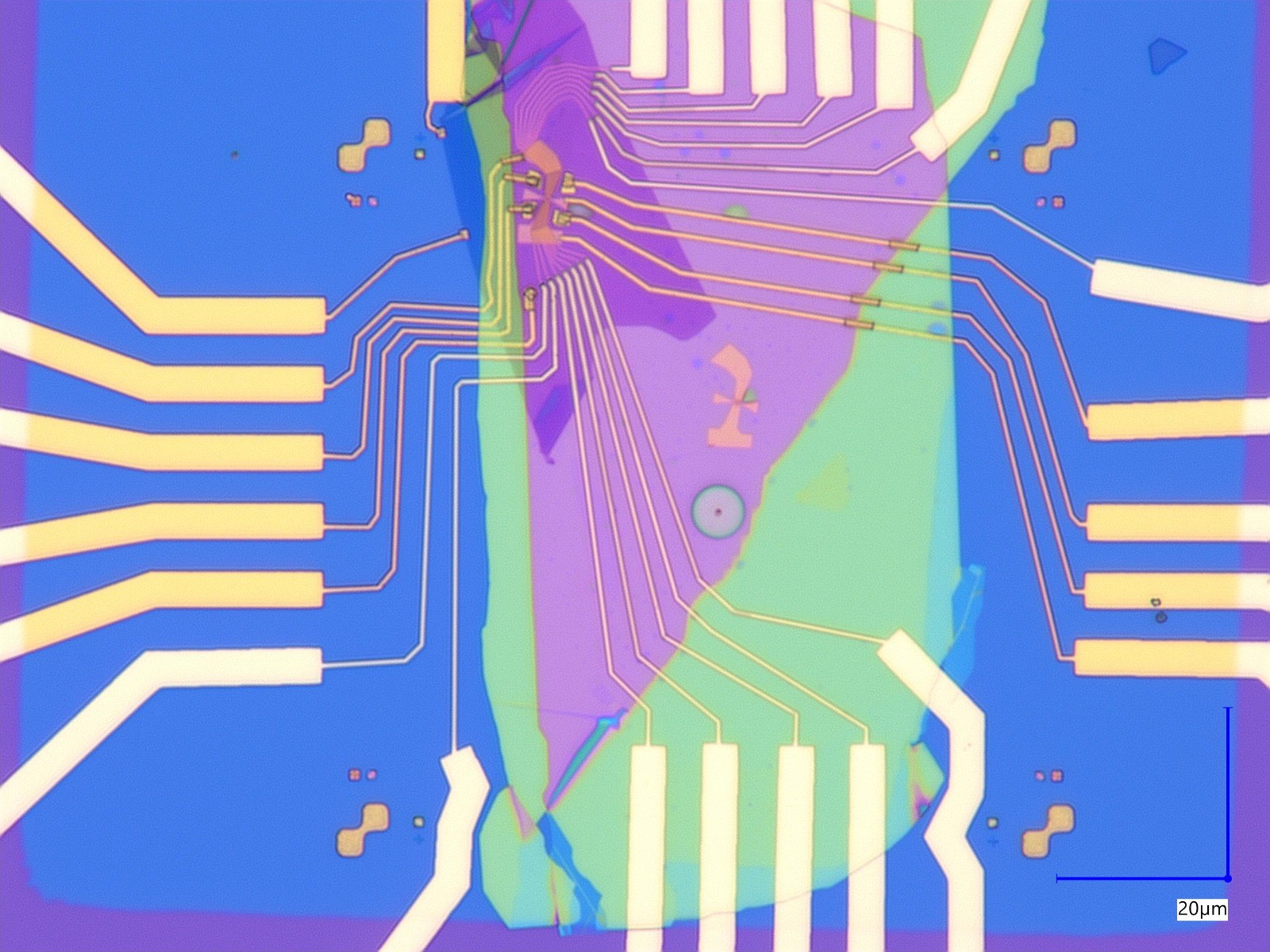
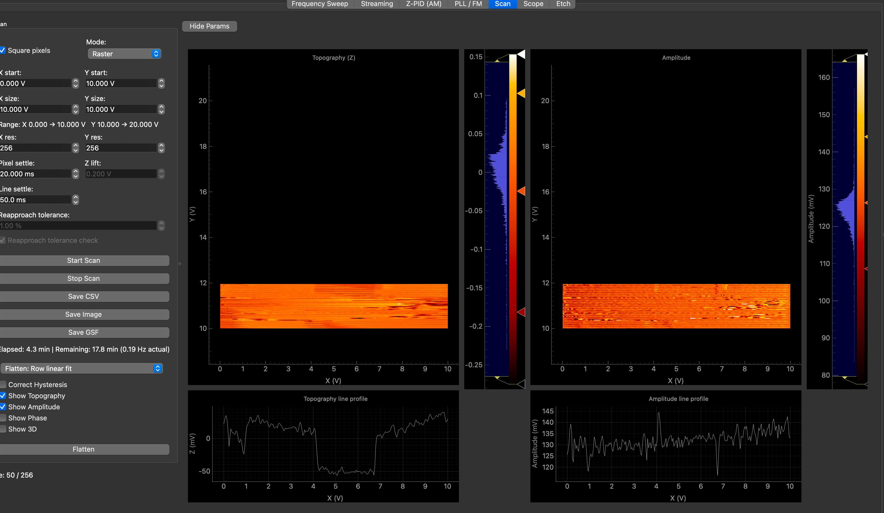 I also imaged the connections wires to a graphene device kindly given to me by a friend where you can see 10s of nm high wires, It's a little hard to see in the topography image without better processing in gwyddion but you can see the e-beam evaporated gold wires coming out from the graphene flake in the amplitude scan quite well.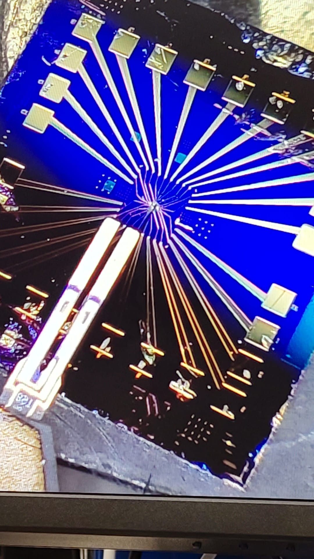
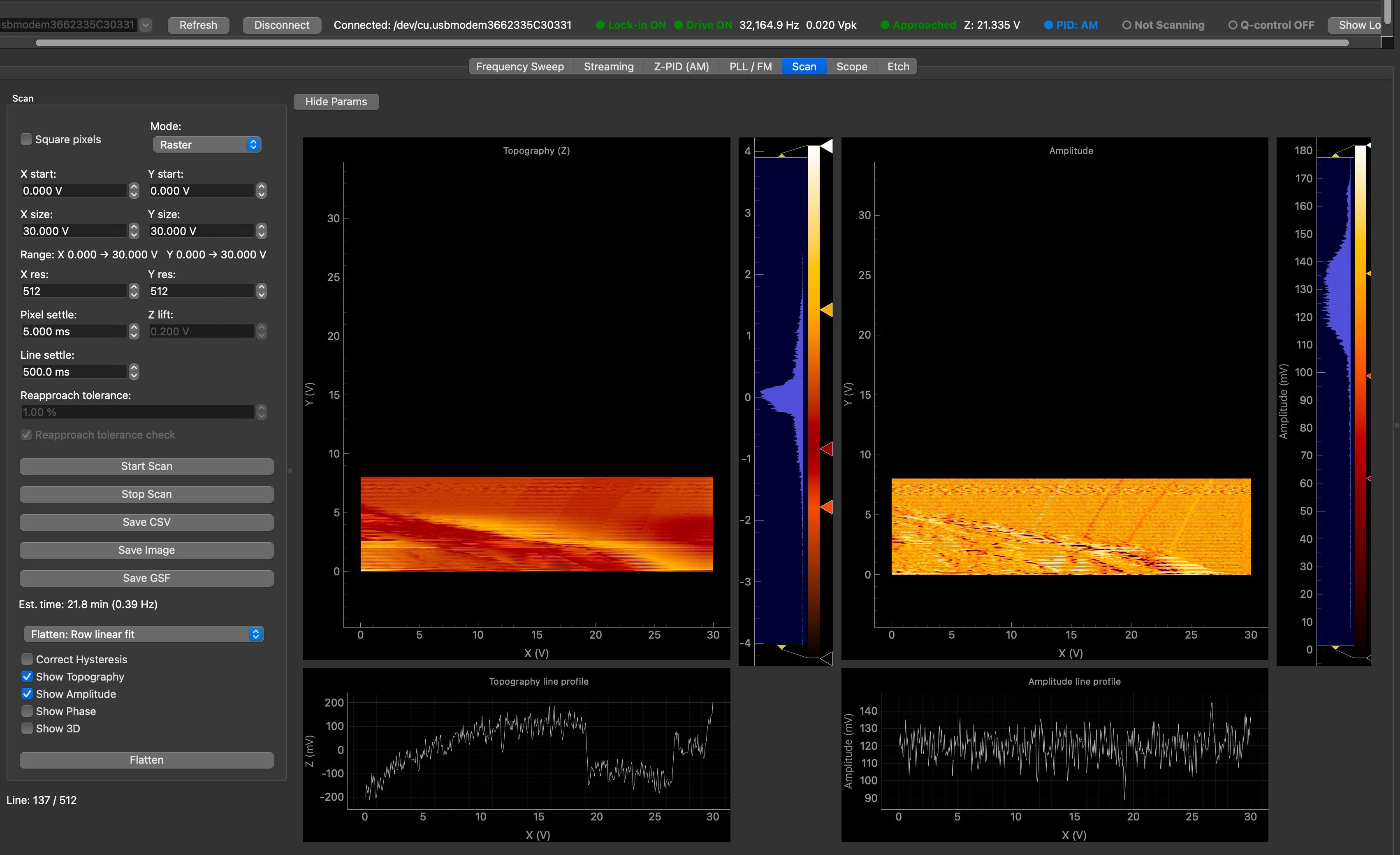 These are all half images because I was trying quite a few things out and I am limited by the bandwidth of my loaded Z piezo buzzer. This means I have to scan quite slowly and the images with high resolution can take quite a bit of time compared to a standard cantilever AFM that will take like 3 min. I actually compared my images to the system we have in the building costing...
 jean
jean
 Abomination named Alex

 Anderson Antunes
 Matt Bradshaw