-
Decoding addresses with MUXes
07/03/2017 at 15:25 • 0 commentstossed out all my wired logic. So the next step was how to replace it with TTL logic. I have one circuit which is particularly irritating. I want to decode the SRC/DST register to know if I need to put that onto the SRC/DST bus, or the POINTER ADDRESS instead. In VHDL, it's very easy:
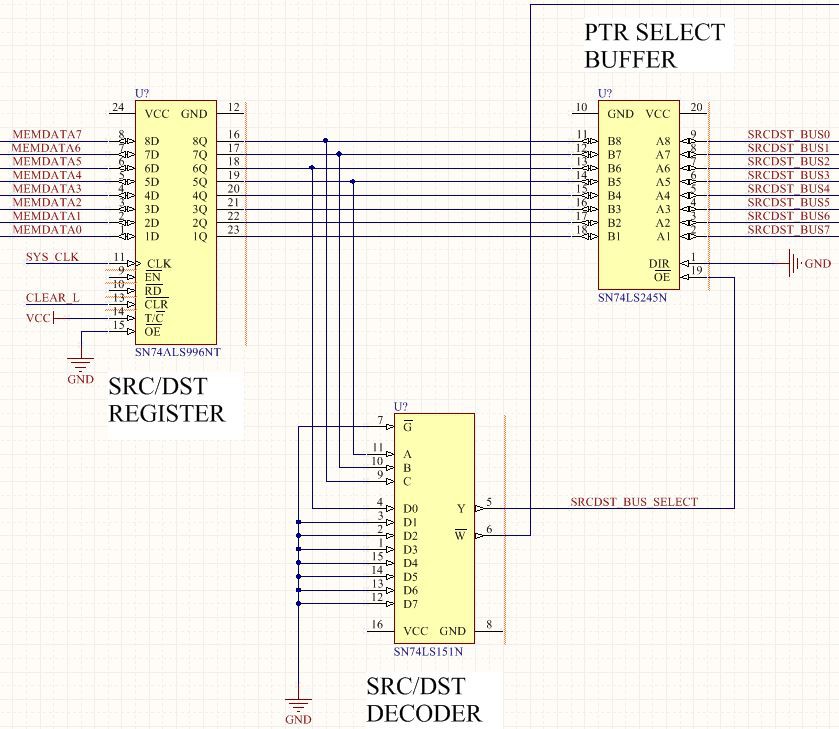
dstAddr <= ptrReg when dstR=PTRDAT else dstR;But I need to do the dstR=PTRDAT logic with chips. I want to do this in only one chip. This proved tricky. My address is x08 or 0x00001000. But I couldn't get the logic down to only one chip (NOR or NAND). There's just too many inputs. So I went with a different approach.I have a lot of free register space, so I decided to use this to make my logic simpler. I'm going to use the address space 0x20-0x2F to be my new pointer data address. This really means my address is 0b0010XXXX. This means I only need to look at the upper 4 bits. This still didn't simplify it enough to put it in one NAND/NOR chip. So I decided to use the MUX method of logic. I chose a 74LS151 8:1 multiplexer chip. Three of my inputs drive the select lines and the fourth is wired to one input. All other inputs are tied low. And there's a bonus inverted output, so one output goes the select the SRC/DST register and the other goes to select the POINTER ADDRESS register (off screen).
![]()
This should be significantly faster than the wired-OR version with transistor inverters (haven't done the math on that yet). And it'll look better and be more true to the TTL goal. If I needed to decode a single address within the 0x20-0x2F space, I could put a second mux in and chain the enable input.
-
Sacrificing good design
06/27/2017 at 12:41 • 0 commentsI had thought I would save some gates by using wired-AND connections in some places. However, they are really slow (relatively). The TTL chips can go pretty fast, and if I add wired-ANDs or wired-ORs, it's going to lower the maximum frequency the device can operate. And I feel like it's not good design. I thought I would try to maintain good design practices and not put hacks in there.
I had another idea to use the '374 chips instead of the '996. Those are 8-bit registers with an output enable, but no clock or load enable. So I was thinking I could just AND the clock with the clock enable. While this is logically possible, it's also poor design. One primary rule to digital design is DONT GATE THE CLOCK, and here I'm thinking of violating that rule. I don't think I can do that.
So I'm reversing some of my bad decisions. I'm going to have to reevaluate my design based on this. I may keep the clock system for now since it's only temporary, and I'm only using that for low-speed operation anyway.
-
One too many?
06/19/2017 at 20:10 • 1 commentI've been going over the optimization steps of my design, and I'm wondering if I have the right approach with a one-instruction set computer. Ultimately, is there much difference between having multiple instructions and multiple source/destination addresses? Decoding my addresses is very similar to decoding an instruction. I technically do have microcode, but it does the same thing every instruction. I still need multiple clock cycles to do memory fetching and execution.
I'm wondering if maybe I could optimize my design by going to a no-instruction set computer. In this case, I would do no instruction decoding at all. The bits of the control path are stored directly as the instruction. So the instructions are then very wide. But if I make my datapath simple enough, maybe it wouldn't be that big. Given that I could have a very large memory, perhaps this is a more optimized path. However, this violates the very root of my project - a one instruction computer driven by data transfers with a memory map. I'll have to think on which direction I want to go. I really want a minimal architecture which can be done with couple dozen TTL chips, but still powerful and flexible.
-
Shoot the engineer
06/19/2017 at 17:43 • 1 commentThere's an old saying that goes "In every project there comes a time to shoot the engineers and start production". Well, ya that's kinda true. We always see improvements and want to make changes. I'm thinking of making a significant change to the project to reduce my chip count and complexity. Right now I have a register for the source address and one for the destination address. And they have their own separate busses and will need their own decoding. These two sections are essentially redundant, so I'm thinking of combining these circuits into one.
The new control flow would go like this:
- Read the source address from RAM/ROM into the src/dst address register.
- Copy the source data into a temporary holding register
- Read the destination address from RAM/ROM into the src/dst address register.
- Copy the temporary holding register into the destination.
Now instead of three clocks per instruction, it will go to four. However, again this could be reduced if the RAM/ROM is not the source or destination. So it could still be as little as two, but requires a little more logic. But it would save at least 6 chips even if I'm adding the temporary holding register. There'd now only be one src/dst address to decode. I want to reduce my chip count as much as is reasonable while maintaining an 8-bit databus. I'll have to archive my project in case it doesn't work out.
![]()
-
Clock improvement
06/16/2017 at 17:28 • 0 commentshe problem with the clock is the switching mechanism. If you change the clock source when the clock has just gone high, some registers may see a rising clock edge and trigger and some may not. This will cause your system to go into an unknown state which is bad. So I changed my switch mechanism to only change when the oscillator is low. I used the two free OR gates to gate my bistable LM555 inputs with the astable LM555 oscillator. I think my clock circuit is finished for now. I'll upload the full schematic as a PDF.
![]()
Improved circuit:
![]()
-
Clock circuit working
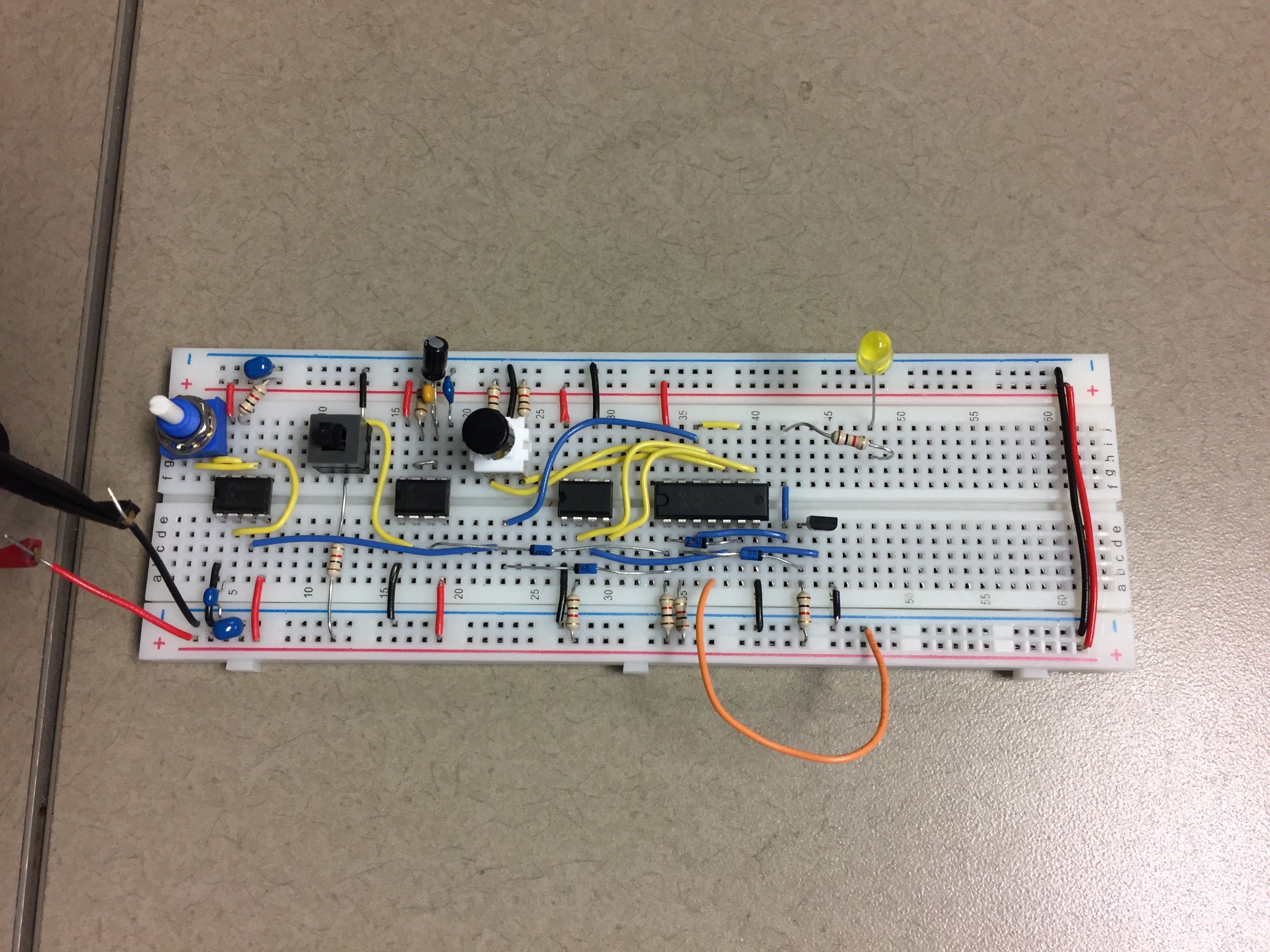
06/16/2017 at 12:36 • 0 commentsFinally got my clock circuit up and running. I'm using a wire for the break signal to check it out. When the break is enabled, it overrides the Select button and selects the Step function. Pushing the step button will then step past the break instruction and then return control back to the oscillator. I'm still not totally happy with how it handles the transition between clock domains, so I may end up pulling all this out and starting over. But not yet - I have way too much else to do.
![]()
-
Revised program counter
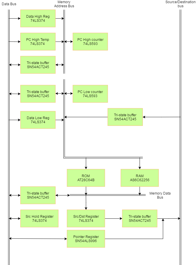
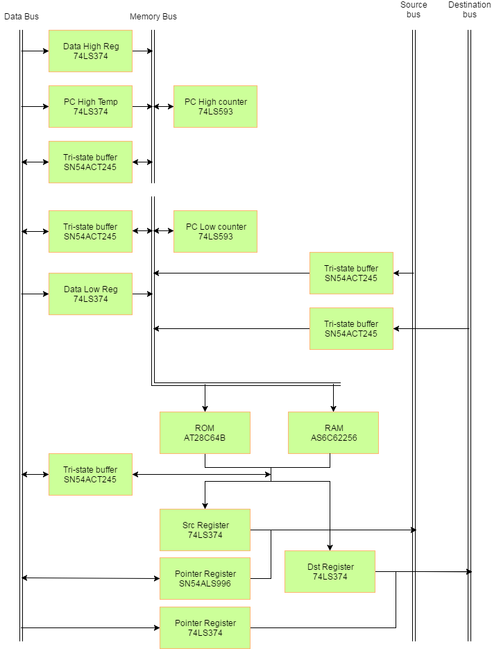
06/14/2017 at 16:13 • 0 commentsI've made some changes to my program counter to incorporate a different counter chip. I found the 74LS593 counter. It's basically the same except it has a single bi-directional bus. This is handy because now I can tri-state my counter output when I want to do data memory access. I ended up completely reworking my block diagram to incorporate it. I needed to add a couple more chips too, but now I believe all of non-control chips are in place. The control logic might be a bit of a bear, but the datapath is nice and clean. I'm also putting together a real schematic, so this is my guide for that.
![]()
-
Clock circuit
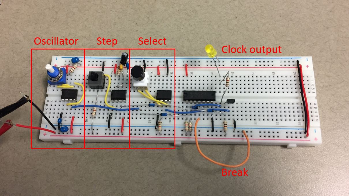
06/13/2017 at 14:23 • 0 commentsI've started assembling the first part of my clock circuit. I decided to partly follow the steps of Ben Eater.
I'll have a variable clock using a LM555, then a push button to step one instruction debounced with an LM555, and then a push button to select between the two debounced with an LM555.
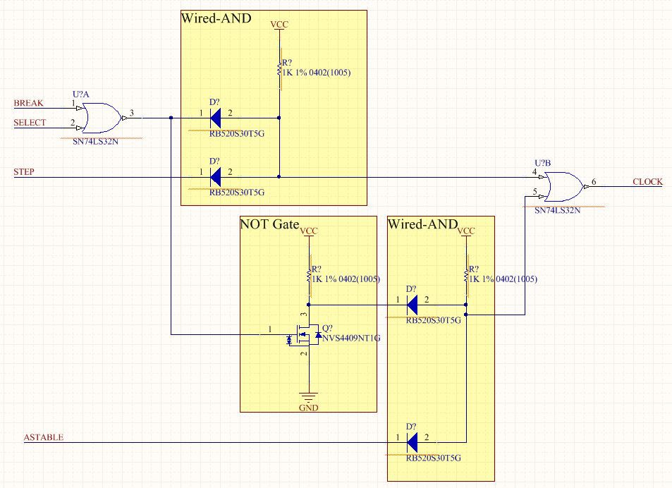
However, I'm departing a bit after that. He has a HALT command to stop the clock until a reset is performed. I think it's more useful to have a BREAK command to stop the clock. The clock can still be manually stepped if the BREAK line is high. This allows you to step past the BREAK command and continue operation. So this can be used as a debug function instead of just stopping the processor until reset. I worked out the digital logic and it looks something like this:
I decided to use two TTL OR gates, and then a wired-AND and a transistor inverter. I chose the OR gate chip because the clock is going to have a large fan-out, so I want a good driver. I could have done the same thing with another chip or two, but this should be more compact. The pull-up style logic will be slower than a TTL gate, but I'll have to check to see how slowly. Eventually I may tap into the UART chip's crystal to provide my clock, at which point I'll want to replace the wired-AND with a real TTL chip. I may be able to pull it off with a single NAND or NOR.![]()
I wanted to add one more thing: this is a bad way to design a clock circuit. There can still be glitches when switching between clock domains. If the clock pulses high, then the select line immediately switches to the step mode, there can be a timing violation in the flip-flops (clock too-short). So some flip-flops will switch state and some will not. I haven't fixed it, but I may later.
-
Bit register chips chosen
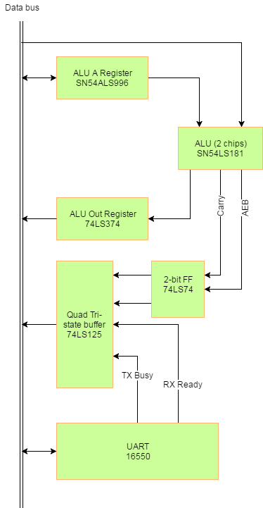
06/09/2017 at 20:00 • 0 commentsI put a little more time into rounding out my chip selection. I needed to include the bit functions (Carry, AEB, UART Tx Busy, UART Rx Ready). I needed flip-flop for the ALU bits, and I needed a tri-state buffer which can turn each channel on or off independently. I put it all into my block diagram so I won't lose track of it. And I hadn't included my UART chip, so I put that in this slide as well. It would be very handy if I had the inverse of all four of these bits, but that would require another buffer chip. I can get by without it in software, so I think I'll save myself the extra chip for now. I don't want this getting bigger than needed.
![]()
-
Assembler problems (and solutions!)
06/09/2017 at 15:53 • 0 commentsI've been putting a lot of time into coding. I've learned some things about writing an assembler:
Problem: If I put a label in a macro and call it multiple times, the same label will appear multiple times. On the second pass, it won't know which is the correct label to jump to.
Solution: Each time I call the macro add a unique number to the label. So I have a static variable in each macro which increments each time it's called. This number gets appended to every label in the macro.
Problem: My macros can overwrite labels. If I put a label right before a macro call, and the first thing the macro does is create a new label, it will overwrite the existing label.
Solution: Error checking in label creation. In my label function, if there's already a label then exit with an error.
Solution: Error checking in second pass. If a label isn't found, then exit with an error.
Problem: No right shift in the 74181.
Solution: Create a left rotate macro. There's a left shift, so I grab the carry-out bit and add it back. Then left rotate 7 times. This is like a right rotate by one. Then to get to right shift, I can do a logical AND with binary 0111 1111. This is the great thing about macros - I now have left rotate, right rotate, and right shift instructions. As I add to my function library, I only get faster and more efficient at programming.
Problem: Need 16-bit increment and decrement operations.
Solution: Macros! I've started writing simple functions for 16-bit operations. Specifically, this is for the stack. I'm working toward push and pop commands, but I need elegant 16-bit operations on the address pointer. But I found another problem along the way...
Problem: Memory access is messy. Especially for 16-bit numbers.
Solution: Standardize memory access with macros. I wrote three macros to access the memory - reading from a destination, writing to a destination, and writing a constant. I've extended this access to 16-bit numbers. I always need 16-bit numbers to be in the same order, so I decided LSB is in the lower address, and MSB is in the higher address. I also arbitrarily change the data ram hardware pointer before every access to ensure even if this is not efficient. I'll make it more efficient later.
Problem: Debug capabilities need to improve.
Solution: Add a macro which converts a byte to two ASCII characters. So I can send bytes out to the terminal to see if the computer is calculating things correctly. I make liberal use of printf to debug, so this is my simple way of doing that. I also want to add this functionality to the bootloader to do the READ memory function.
Problem: Software is not flashy. I don't have interesting pictures on my blog.
Solution: Seriously get started on my TTL hardware. This was a big goal of the project, so I really need to get away from the FPGA. It's just so easy to stick with an FPGA and I can simulate to help debug. But I've reached the point where I can load program easily to RAM and even create a ROM program easily to create test code for the TTL computer. And I have a good hardware and software simulation of it, so I can check my test programs too. I guess it's time to pull the trigger.
One-instruction TTL Computer
A breadboard-able computer which uses only a single instruction - MOVE