-
Covered Photomultiplier
02/01/2019 at 18:16 • 0 commentsIt is a long time ago, since my last log entry. The main reason for this, is that I moved from the US back to Germany. Therefor I was busy to find a new apartment and I had to wait for the container with all the stuff in it. Further I had to find a makerspace in my neighborhood with a laser cutter. I found one in Wiesbaden ( Makerspace).

The image above shows the principle approach how I want to detect secondary electrons. My previously design I wasn't able to detect anything. I had to much stray light and everything was a little bit shaky.
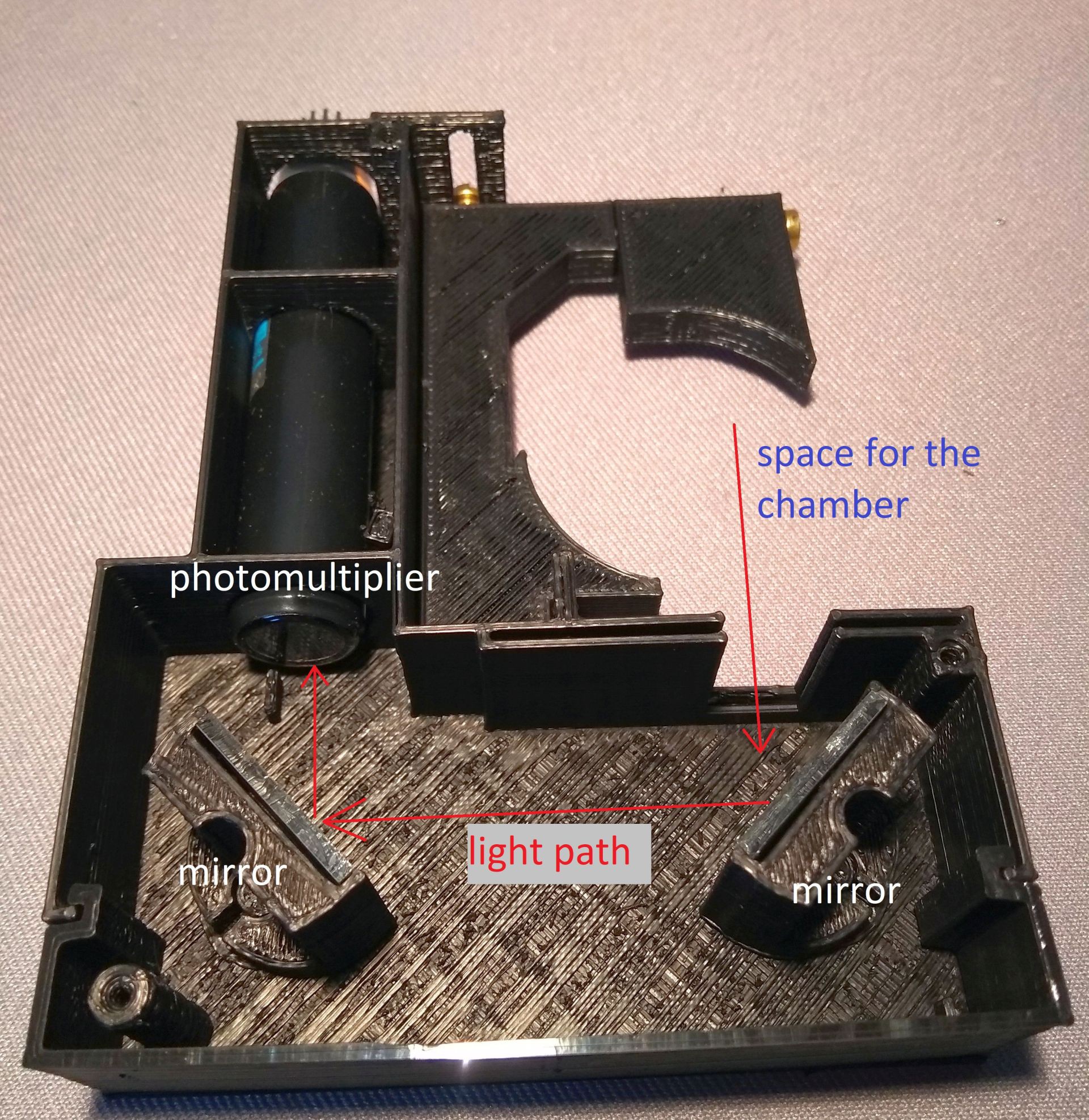
Therefore I updated the design which is shown in the image above. In the right top corner is the space for the chamber with the sample in it. The light from the detector screen go straight to the first mirror and then to second mirror which guide the light to the photomultiplier.

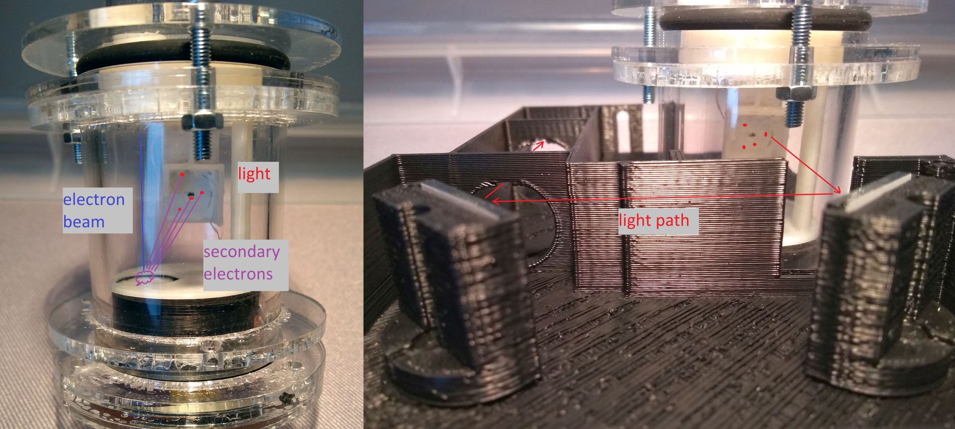
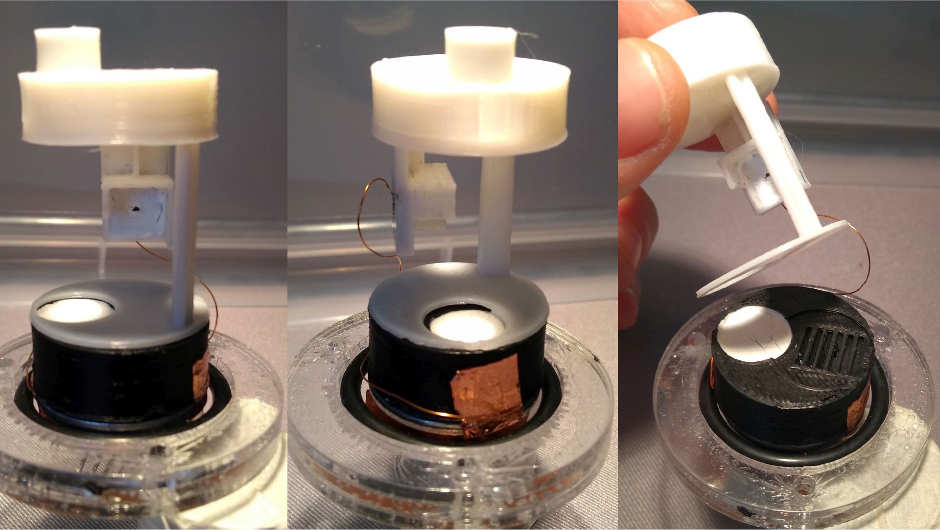
In the image above on the left side is the chamber shown and on the right side the chamber assembled in the detector arrangement. The electron beam come from the top of the chamber and hit the round area where the sample is. Secondary electrons are created symbolized by the purple cloud. The secondary electrons are attracted from the black spot which is conductive plastic. Hopefully, some electrons will hit the detector screen and create a reddish light. This red light follow the light path guided from the mirrors.

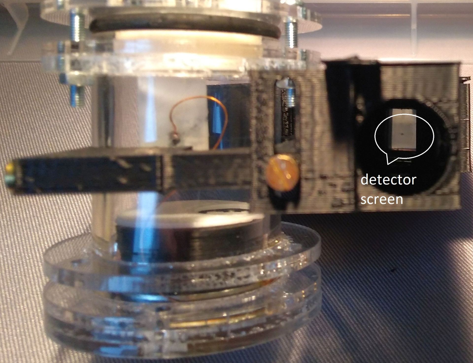
In the image above is the view from the photomultiplier shown. In the right part is the detector screen through the mirrors visible.

In the image above are the parts in the chamber shown. On the left side is the front view. The detector screen with the black spot is visible. In the middle is the side view. It can be seen that the detector screen is covered from the top and side. Just the bottom side is open to increase the likelihood that only secondary electrons for the sample are attached. On the right side is the sample holder shown. The with round are is a detector screen to visualize the electron beam and on the right side is a test patter.
-
Detector Photomultiplier
07/30/2018 at 14:36 • 0 comments
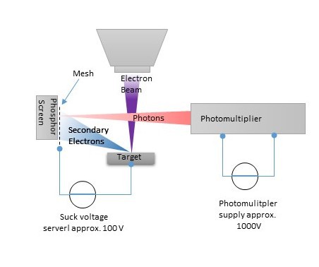
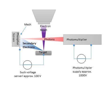
The image above show the new design which shall me enable to get a image out of my DIY SEM. The idea is that a voltage is applied between the target and a mesh in front of a phosphor screen. The secondary electrons are accelerated in the direction of the mesh. Some electrons hit the mesh and some other will hit the phosphor screen. Actually it is a screen made of a zinc sulfide. When the electron hit the screen photons are created. This photons will fly to the photomultiplier which convert the photons to electrons and multiplies these by 1.000.000.
The image above show how it looks in the reality. The black long tube on the left is the photomultiplier. The withe piece behind the wire is the phosphor screen.

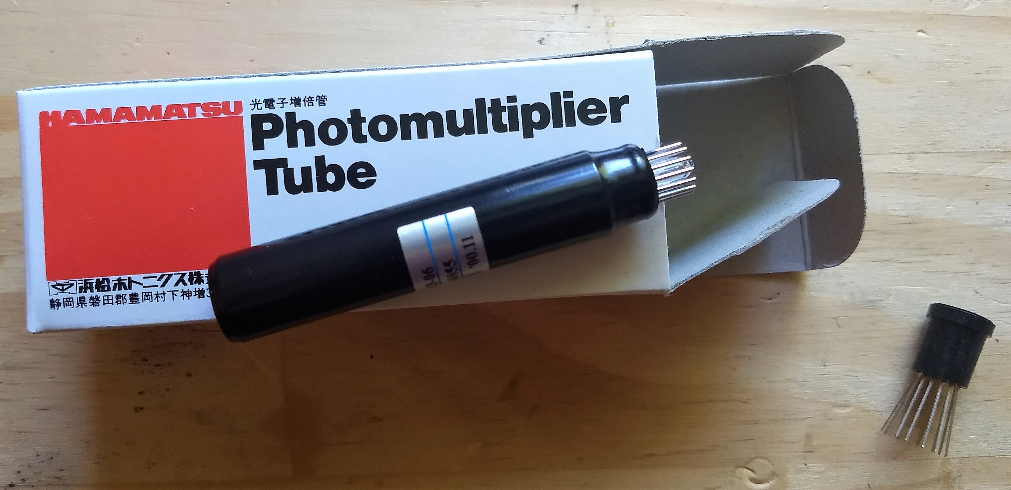
I found my photomultiplier above (HAMAMATSU R1463-06) on ebay.

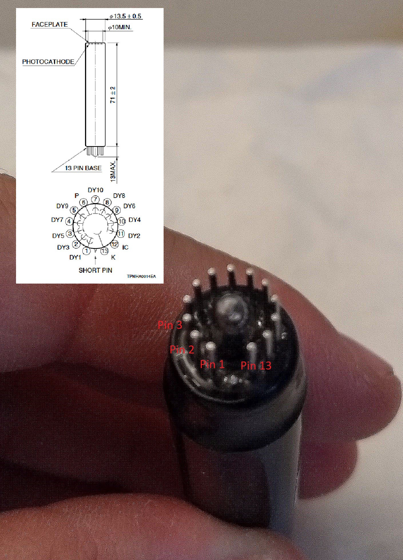
The image above shows the photo multiplier pinning.
Further I found I nice video from 1959 what explains how a photomultiplier works.

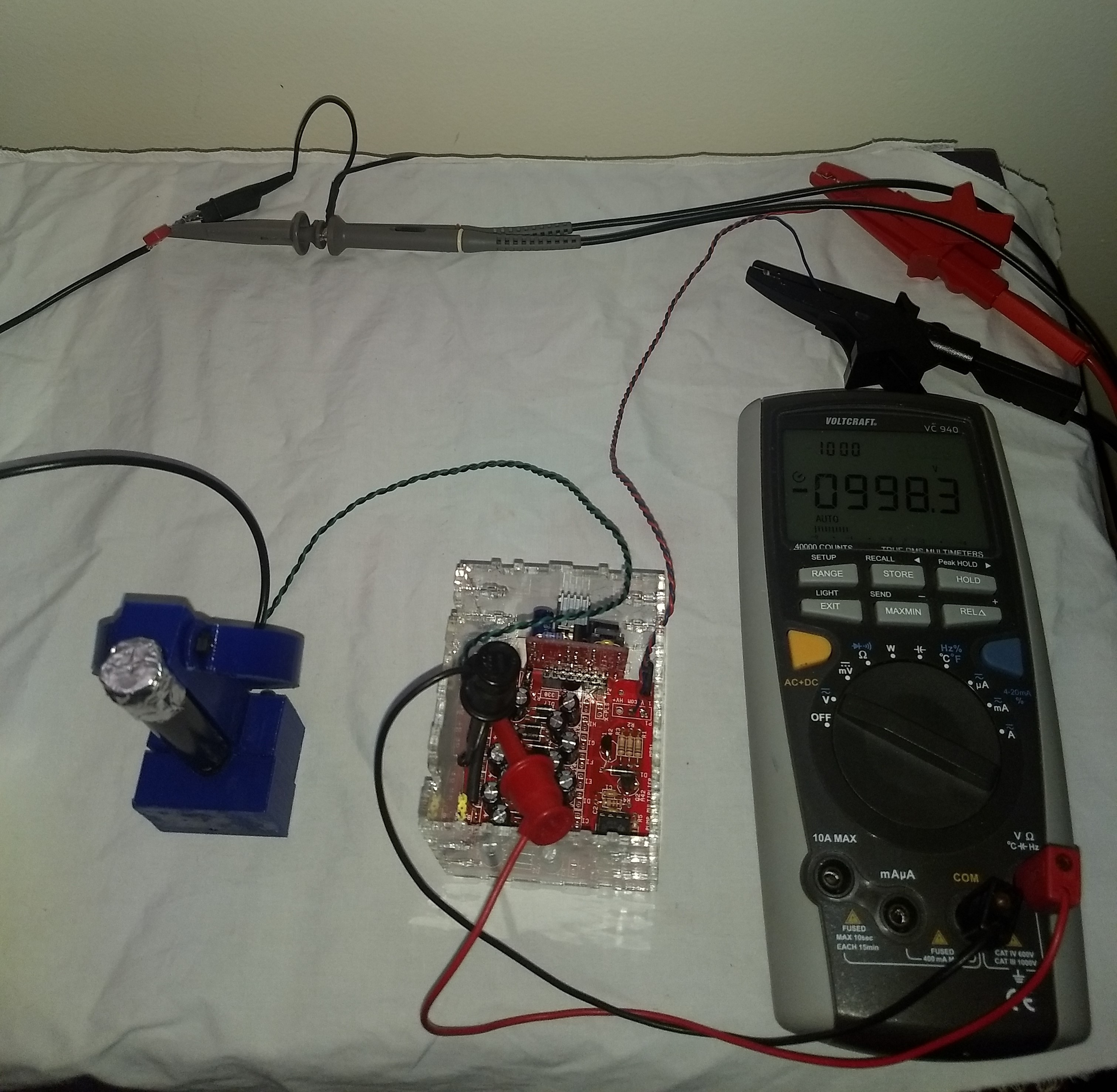
The image show the supply voltage of the photomultiplier .The red PCB is a set-up convert which convert 12V in up to 1450V.

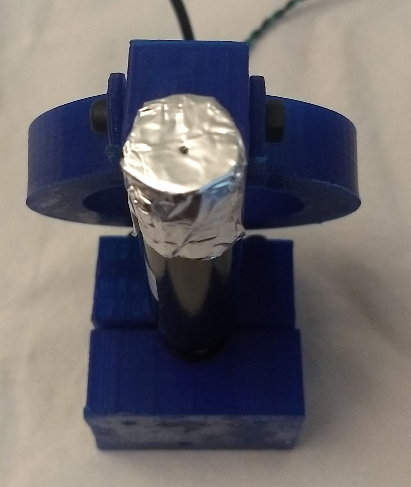
Above on the image is shown the photomultipler with aperture. The piece of aluminum foil has a small hole in it. This is necessary to prevent that the photomultiplier saturate.

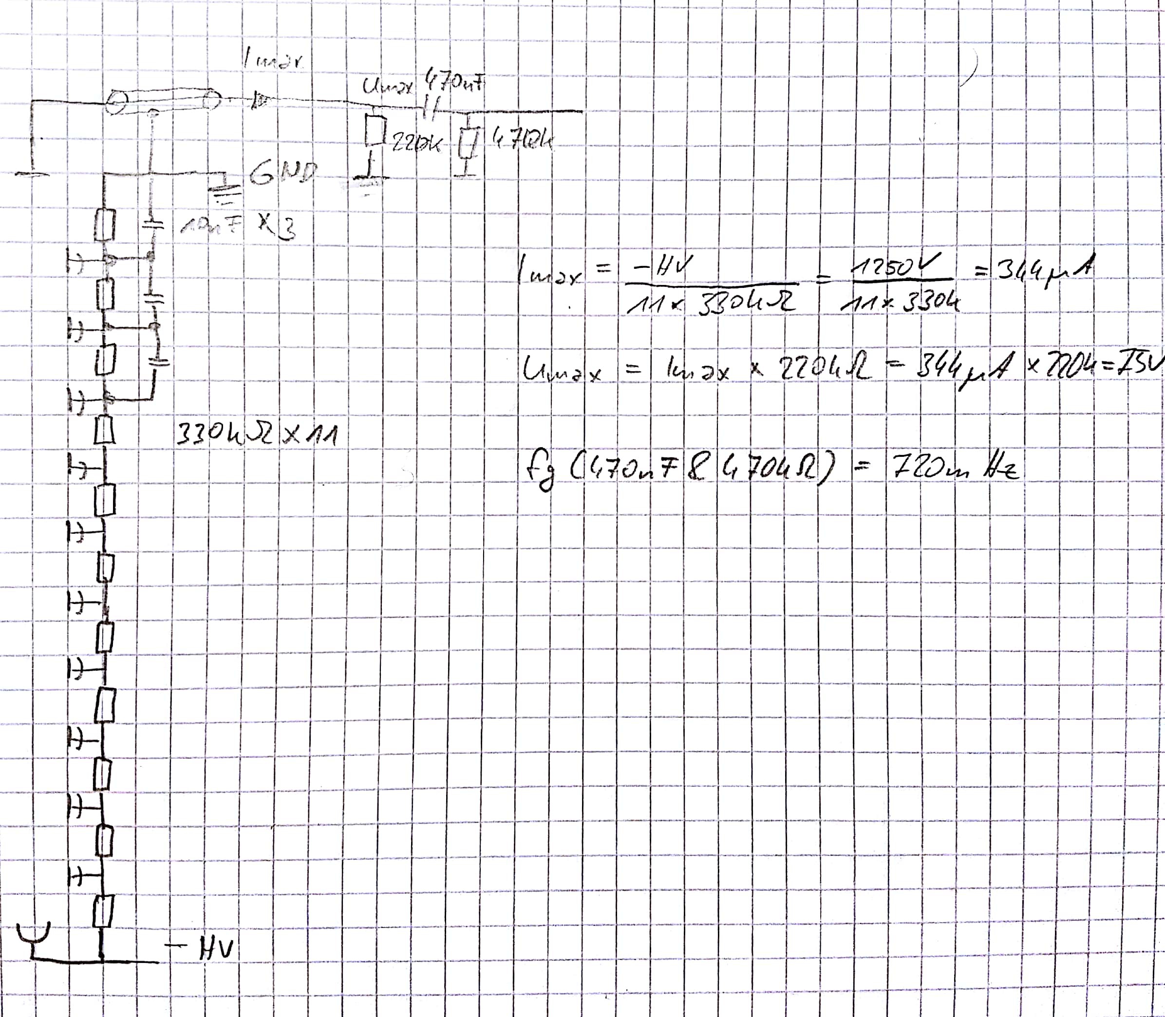
The schematic above shows the components which are required to operate a photomultiper. The negative high voltage (-HV) is divided by 11 x 330kOhm resistors. The current through the divider is 344µA @ 1250V. According to a handbook of Hamamatsu (https://www.hamamatsu.com/resources/pdf/etd/PMT_handbook_v3aE.pdf) shall be the signal current below 1/20th of the divider current. At the out is a 220kOhm resistor to limit the maximum output voltage to 75V@344µA. At the end is a high pass filter with 470nF and a 470kOhm with a cut of frequency of 0.72Hz.
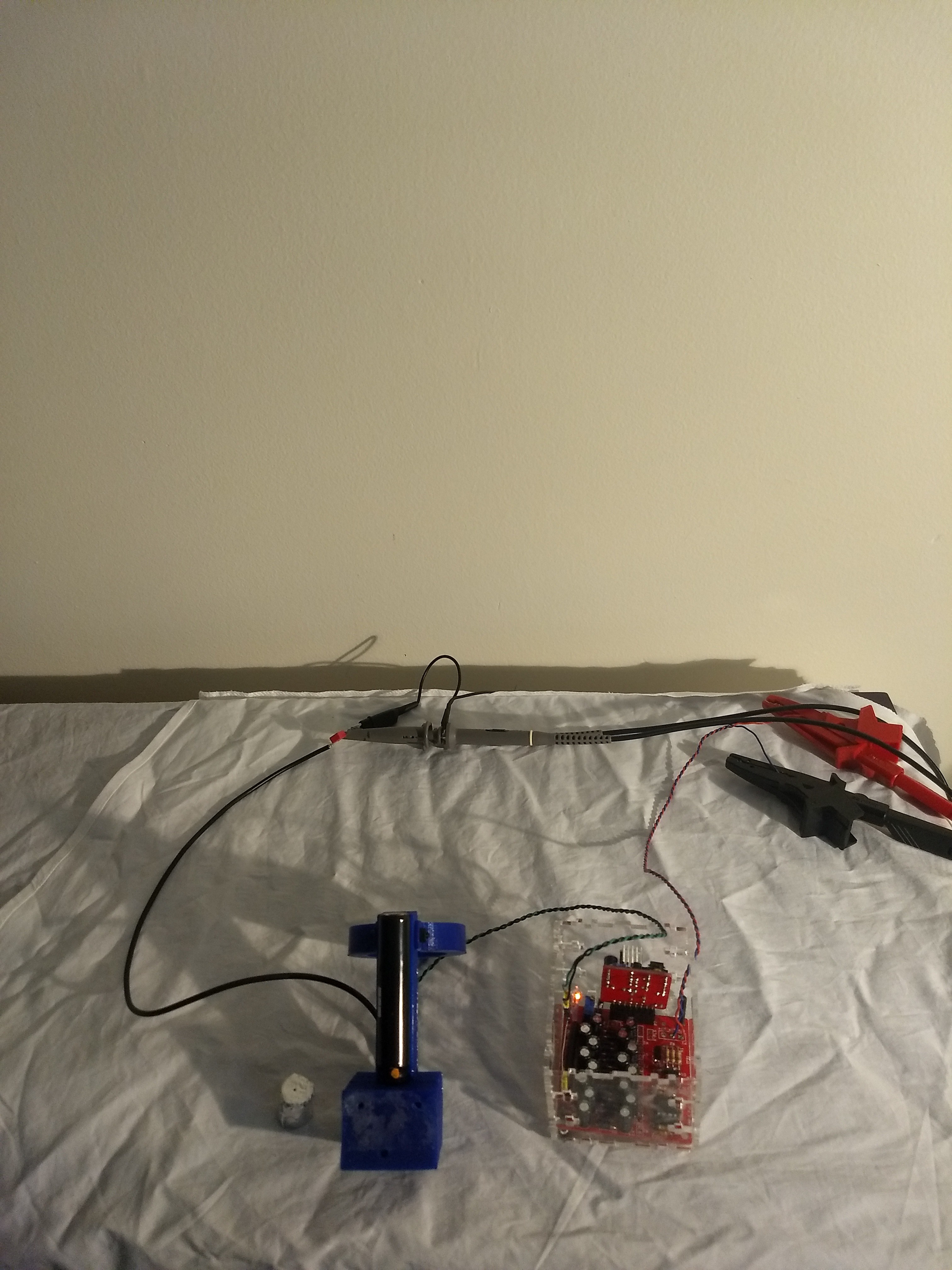
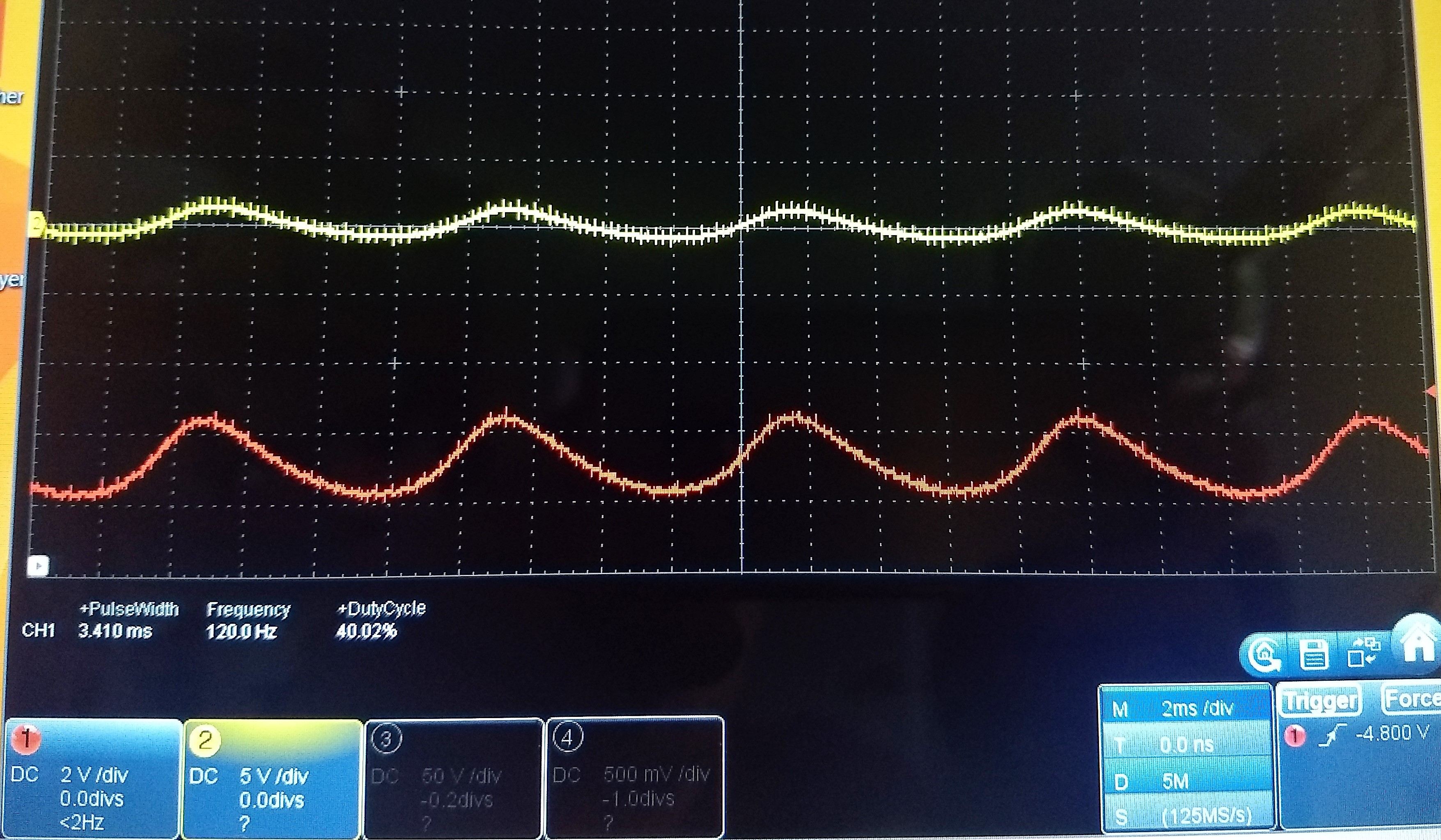
 One of my first test was just to point the photomultipler to the wall and illuminate it with my desk lamp. In this test I figured out that i need an aperture.
The yellow signal is behind the high pass and the red one is before. In the signal can be seen that my desk lamp has small flickering.

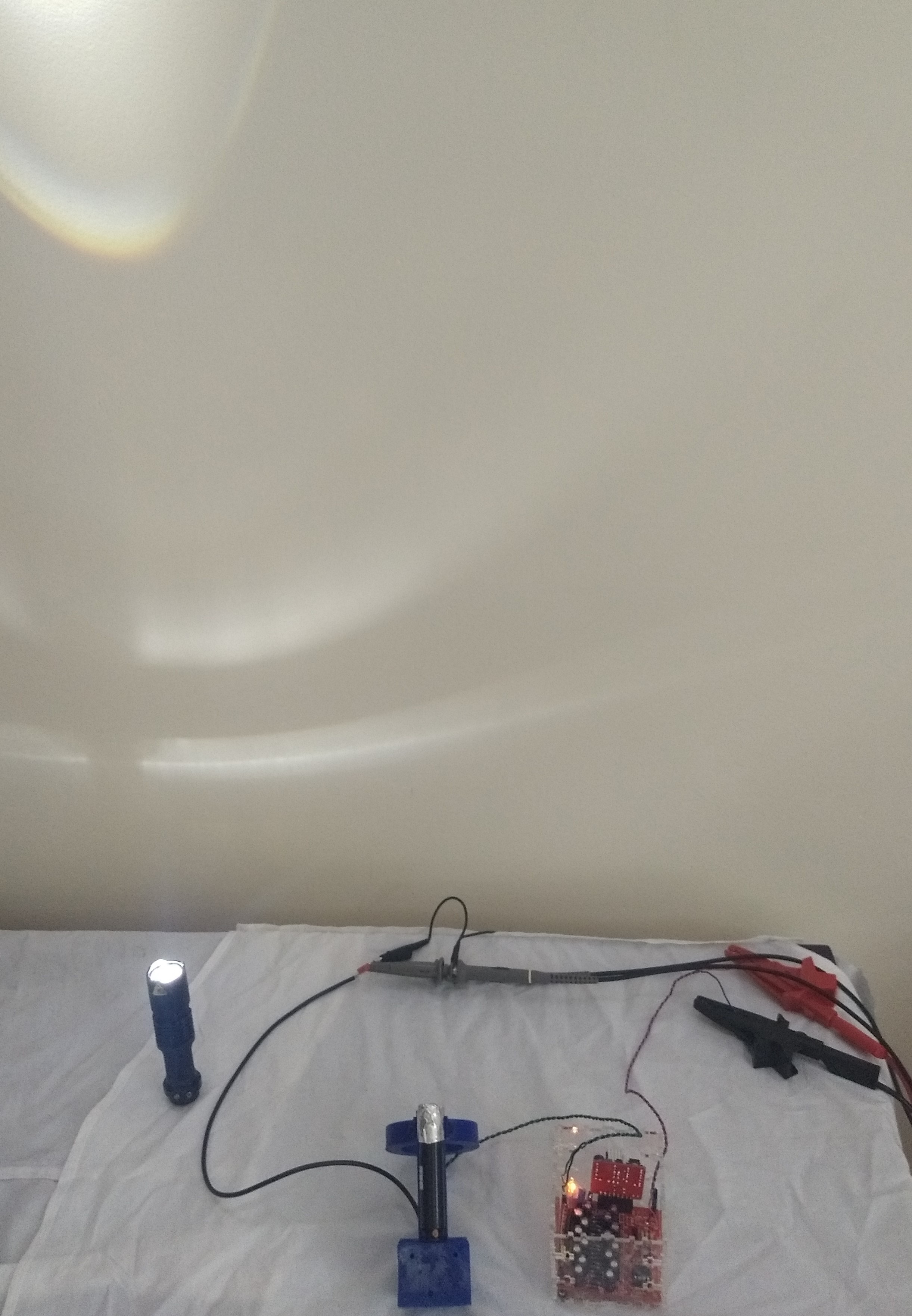
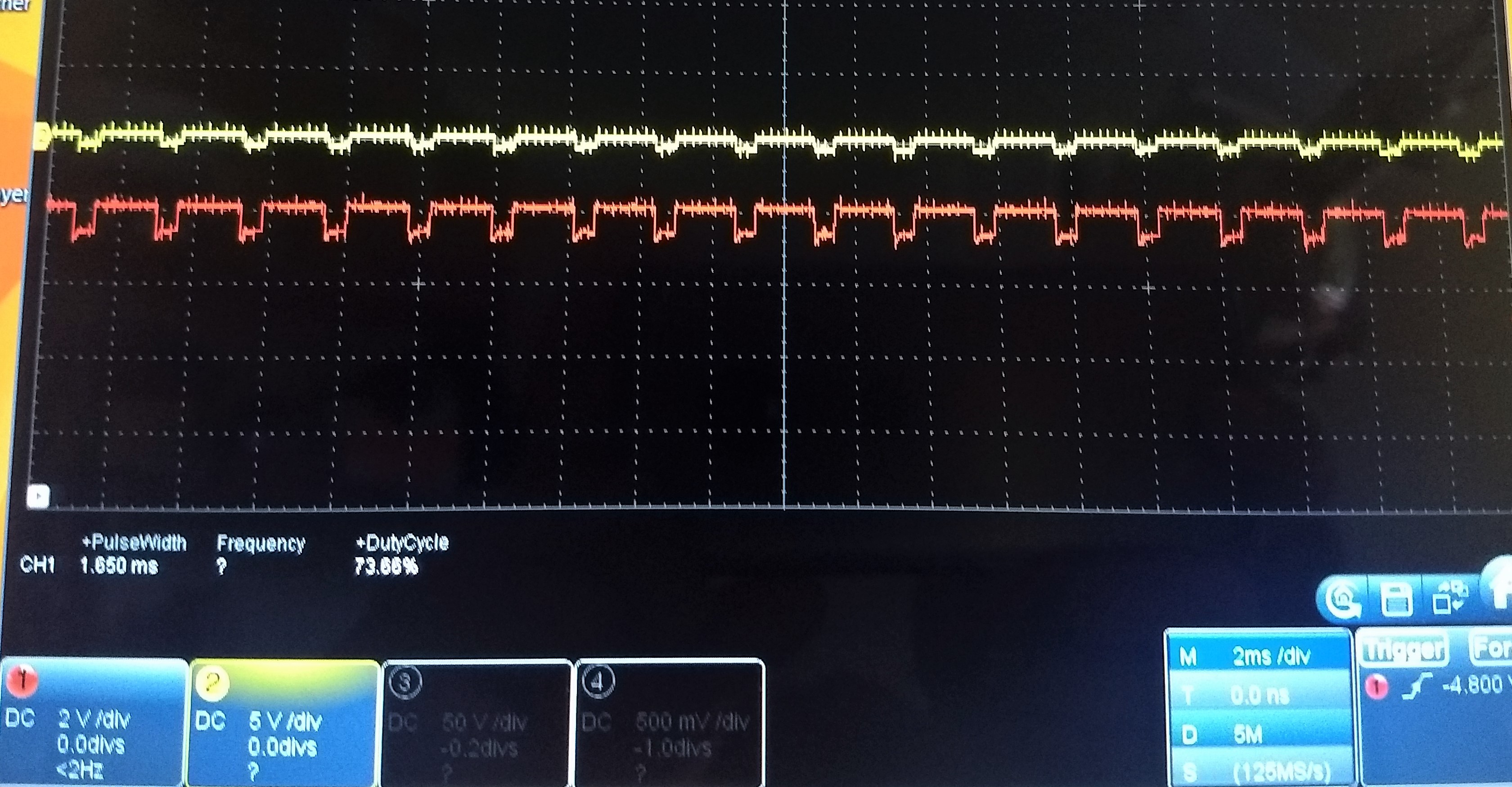
In the image above is my second test setup shown with a LED flashlight. The flash light was in a dim mode.

The signal above shows in yellow the signal after the high pass and in red before. The signal show good that the LED flash light use a PWM signal to dim the light.
-
EMC Shielding
06/08/2018 at 14:00 • 0 comments
The image above show the current detector design which I have to reconsider because of shielding issues.
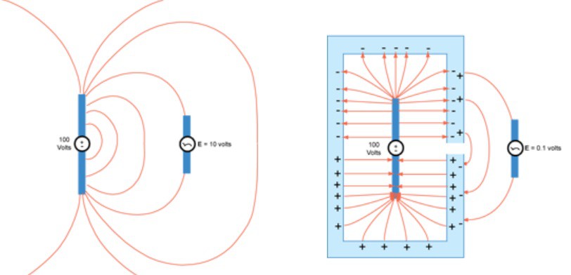
https://learnemc.com/practical-em-shieldin The image above show how a shielding against a electrical field works. Please have a look on the page LearnEMC which explains quite well the background to shielding.

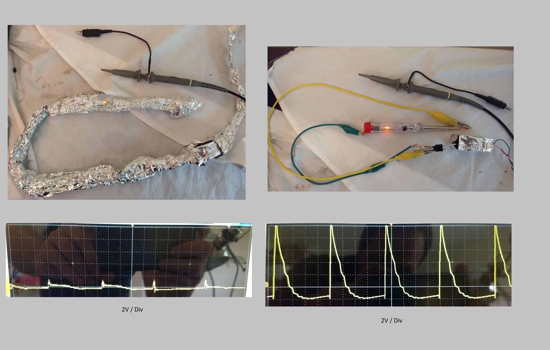
In the image above I show how the shielding issue looks like. in the right corner, I connected the high voltage supple with the yellow and green cable. At the end of the cables I connected a screw drive with at voltage indicator. This voltage indicator is actually a glow lamp with a resistor. I placed the tip and the ground of scope close close to cables. In the right bottom, is the image of the scope shown. The image shows voltage peaks with approx. 12V. In the left corner I covers almost everything with aluminum foil. I left only a small hole to see the glow lamp. I was also important to cover the low voltage cables to the high voltage supply to get the best result. After all the effort in the left bottom corner is the result shown. The voltage peaks decreased to approx. 2V.
Maybe the shielding issues are the reason that photo multiplier are so popular.
-
Detector plates
05/11/2018 at 15:27 • 0 comments
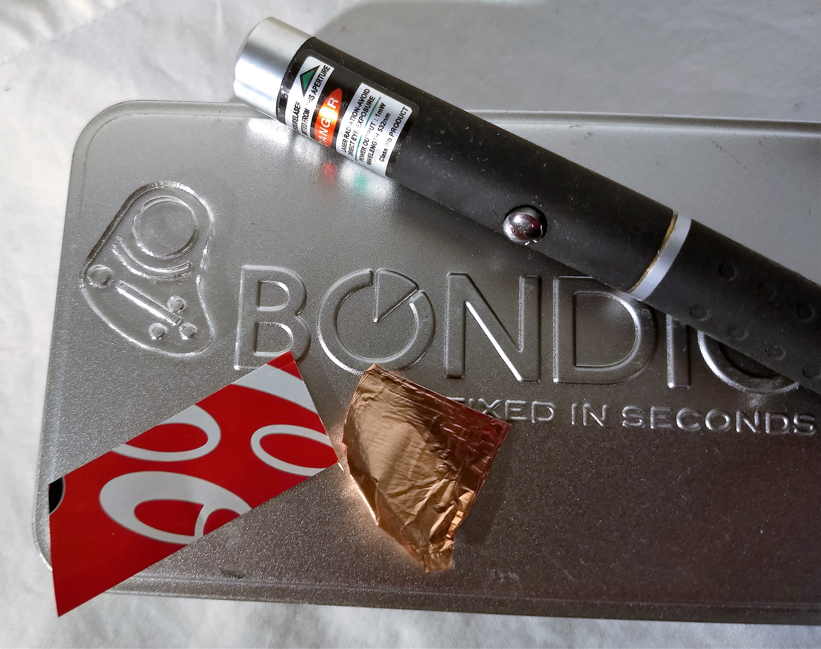
On the image above are the materials shown which I used to build the detector plates. With the laser cutter I made a support out of acrylic. I used sticky copper foil for the accrual detector plates and a piece of a soda can to make it stiffer. The laser pointer is a blue one and is great to cure UV glue.

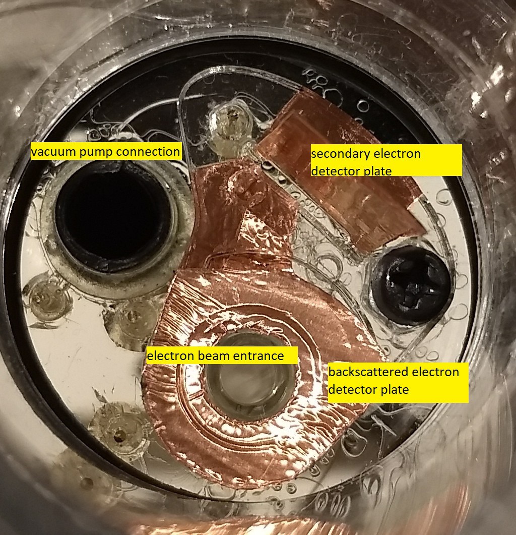
On the image above are shown different views of the detector . The foil with the hole in it, is for the backscattered electrons. The last magnet of the lens system is glued direct to the foil. The rectangle foil is for the secondary electrons. This piece is reenforced with the soda can and glued with two tiny spots of UV glue.
Below the image show a view in the chamber with assembled detector plates. The black screw is made of nylon.
-
PC Software
04/16/2018 at 20:59 • 0 comments
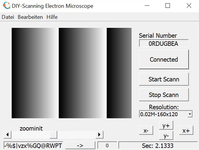
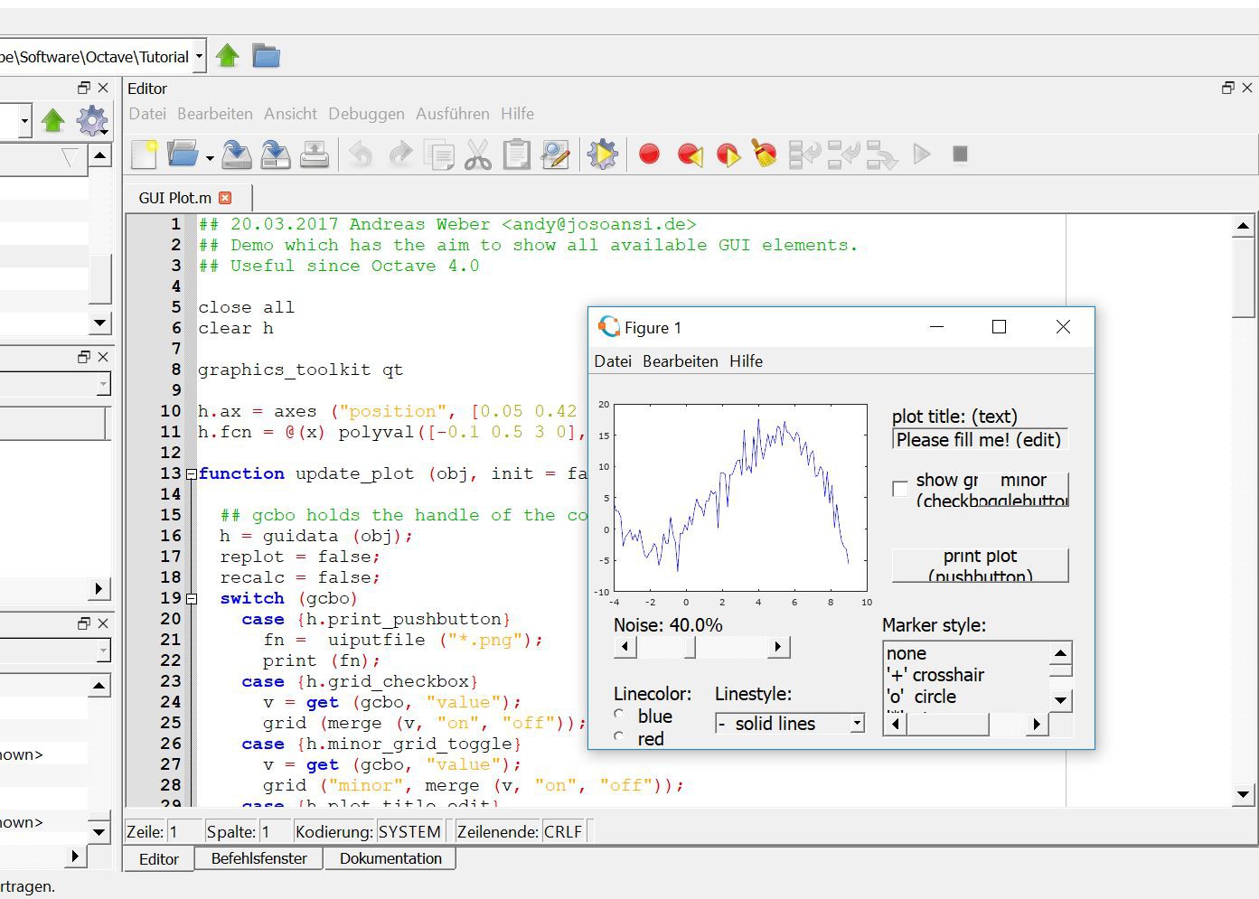
The first communication test between the microcontroller and the PC was successful . The microcontroller transmit a chaining gray value and the GUI shows a image. The GUI was make with GNU Octave. In the following I describe what the program do.It is quite ease to program it, if you know all the needed commands. So I hope the following helps somebody who is looking for: Octave GNU receive serial data, convert string to array, convert string to matrix, change size of a matrix, change size of array.h = serial("\\\\.\\COM6"); % Open the port srl_flush(h); % clear the buffer data = srl_read(h,200000); % read data from serial interface serialstring=[serialstring,data]; %add the new data to the buffer serialstringThe code above is for Octave GNU. It opens the serial port, read data from the serial port and add the data to a buffer.
The image above visualize how the buffer content looks like. The buffer contains random data like "BEEF.." then transmit the micro controller a header like "480 Hello_World" and the data of for example ADC chanel1 and ADC channel 2 in a 16 Bit format.
header=[typecast(uint16(resolution.x),"Hallo_World")]; % create a header for the search
matches=findstr(header,serialstring); % search the header in the buffer and return a array of matches
serialstring=(serialstring(matches(1):end)); % remove the date befor the frist header
The code part above creates the same header in Octave GNU as the micro controller transmits and search this header in the serial sting. The last line removes everything before the first header appear.
The image above shows how the buffer look like after run the line of codes.
serialstring=typecast(serialstring,"uint16"); %convert the buffer to uint16 because the microcontroller send uint16 too
matches=findstr(typecast(header,"uint16"),serialstring); % search the header in the 16 Bit buffer
The two line code convert the 8Bit serial sting to 16bit values and search again for the positions of the header because the previous positions were for a 8 bit buffer.
The image above shows how the buffer look like after run the line of codes.
% the image has as many rows as header exsist
% the length of a row is the distance between tow heade
imag=reshape(serialstring,matches(2)-matches(1),length(matches)); % create a imag
The line of code convert the 1D sting in a 2D array.
The image above shows how the buffer look like after run the line of codes.
% the microcontroller send two channes
imag_ch1=cast(imag(14:2:end,:),"uint16"); %remove the header and take each second value
imshow( imrotate (imag_ch1,90)); % rotate the image by 90°
The two line code above remove channel 2 and the header from the image. The last step is to rotate the image about 90° in show it.
The image above shows how the buffer look like after run the line of codes.
-
PC Software
04/06/2018 at 02:04 • 0 commentsGNU Octave
For the PC software I choose GNU Octave. A very powerful math tool kit with a option to include a graphic user interface. The download link for octave. Also very useful are the big variety of additional support packages on this page . I use the instrument-control package which contain the driver to user the serial interface. A useful descriptor for use the serial interface is this page https://www.edn.com/design/analog/4440674/Read-serial-data-directly-into-Octave.
The above linked video series gave me a introduction to Octave GNU.Andreas Weber example code was very helpful to understand how a GUI in Octave is build.
h.plot_title_label = uicontrol ("style", "text",
                                "units", "normalized",
                                "string", "plot title: (text)",
"horizontalalignment",
I struggled a little bit until I understood that with (h.xyz = uico(...)) ui elements are placed.
 h = guidata (obj);
...
  switch (gcbo)
...
...
guidata (gcf, h)
guidata store the handle of the ui elements and guidata and gcbo gives the handle back in the function.
Another big challenge is to create a timer which calls periodically a function. I found a good approach on the following page https://savannah.gnu.org/bugs/?32316. The approach is to use the event hook to call a function. I was able to call the function about every 100ms.
-
Electronic PCB
03/16/2018 at 13:36 • 1 comment
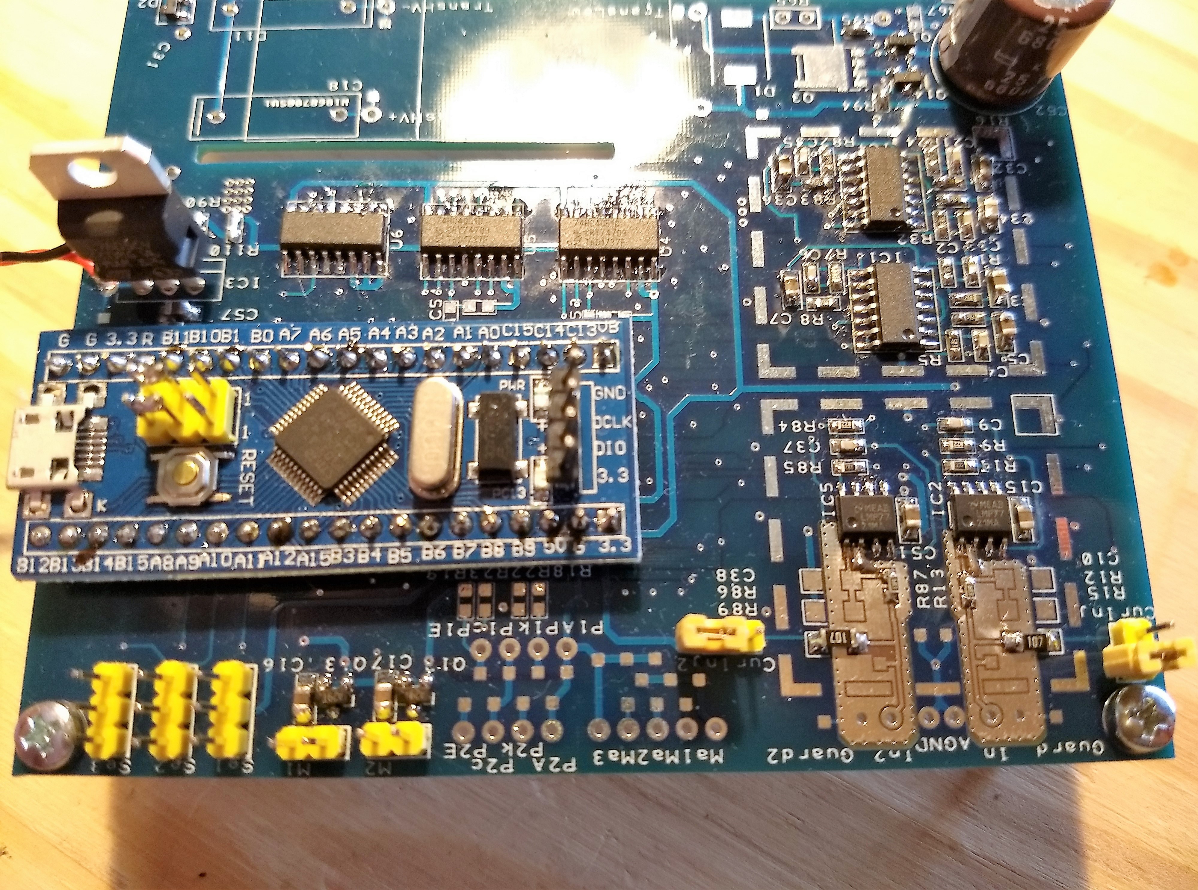
On the image above it the PCB shown which I made. I right lower corner of the PCB are the Femto ampere amplifier placed . The plain area surrounded with vias are the guard ring as I describe in the last log entry. On the guard ring is the solder mask removed to get the bare resistance of the FR4 base material and don't "short" the FR4 resistance by the solder mask . The square pattern around the Femto ampere amplifiers are for a EMI Gaskets to improve the shielding for the case that I run in to EMC issues. In the square pattern above the Femto ampere ampere amplifiers are placed the secondary amplification stage with the MAX4450.
-
Detectorelectronic
02/21/2018 at 03:11 • 0 comments
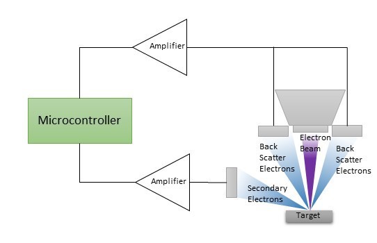
The image above gives an overview how the electrons are collected and detected. The incoming electron beam triggers two types of electrons: the Back Scatter Electrons (BSE), which fly backwards along the beam and the Secondary Electrons (SE), which stay close to the target and don't move. Charged plates are located both above and alongside the target. The image below shows how a picture looks with BSE compared to SE.

http://www.ammrf.org.au I expect that the BSE and the SE current to be measured will be quite low. Therefore, I had to look for an amplifier with a very low leakage current of the inputs. I am glad that I now found femto ampere amplifiers for an affordable price. The LMP7721 from Texas Instruments and the ADA4530 from Analog devices. Both companies have several application notes which explain how to use these amplifiers.
Above is shown the whole schematic I created to measure the BSE and SE. In the next paragraphs I explain each part in more detail:A: This section shows the Femto ampere amplifier. The opamp is configured as a non-inverted amplifier. The reason is that with a configuration as a inverted amplifier it is hard to get a broad band width. For example a 1 GOhm resistor with a 1p capacitor in parallel would result in a cutoff frequency of 160Hz (f=1/(2*PI*1G*1p). Further The amplification is set to 2.48 (8.2k/3.3k=2.48) for stay in a comfortable area of the GBW (Gain Band Width) of the opamp. The 10p capacitor set the low pass cutoff frequency to 1.94MHz (f=1/(2*PI*8.3k*10pF). The virtual ground (VirGnd=3.3V/2=1.65V) is set to the half supply voltage of the micro controller. The applied VirGnd voltage appear at the +input of the opamp and make it possible to measure even negative current with just a single supply of the opamp. The 6k8 resistor in the input line limits the current in the case of activating the opamp internal ESD dioses. The 6k8 builds with the opamp internal capacity a low pass with a cutoff frequency of 2.12MHz ((f=1/(2*PI*6k8*11pF)) .
B: This section shows the secondary amplifier. The Max4450 is a high speed opamp and has a band width of 175MHz. This make it possible to get amplification of 14,4 (Av=56k/3.9k) at 1MHz. The high bais current of 6.5µA requires to configure the opamp as a inverted amplifier, because in the configuration as non-inverted amplifier is it challenging to get a stable virtual ground. The low pass cutoff frequency of each opamp stage is set 2.4MHz ((f=1/(2*PI*56k*1.2pF)) . The 10µF input line creates a high pass with a cutoff frequency of 0.27Hz (f=1/(2*PI*{56k+3.9k}*10µF). This high pass blocks the DC voltage of each previous stage.
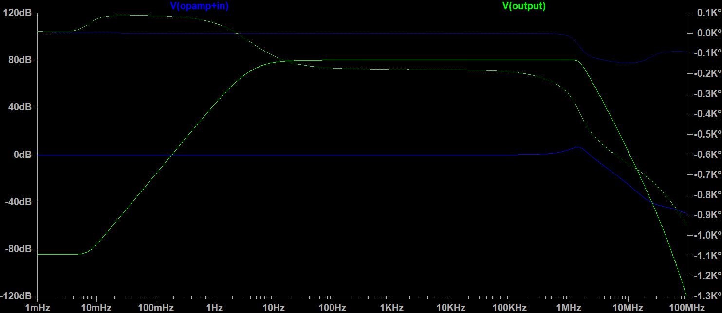
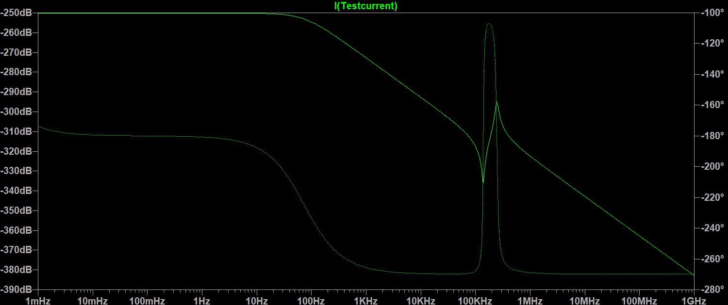
The image above shows a bode plot over the whole amplifiers. The blue line is the signal at the +Input at the LMP7721 of section A and the green line is the output at the last MAX4450 amplifier of section B. The plot illustrate the whole schematic creates a amplification of 80dB. This mean that a 1 Femto ampere make a output of 10mV (U=I*R*Av=1fA*1G*10000).
C: This section shows the guard amplifier. For measuring Femto ampere is a addition shielding required, which is in chapter 8.1.1 of datasheet of the LMP7721 described. The approach for this shielding is to surround the high impedance input of the femto ampere amplifier with a signal which has a equal potential but lower impedance. Analog Devices gives in the chapter Layout Guidelines of datasheet ADA4530 a good overview. The actual guard amplifier is a non-inverting amplifier connected to the -input of the Femto ampera amplifier.
D: This section are just symbolizing the power supplies . The 5V power supply is for the amplifiers and the 3.3V for the virtual grounds.
E: This section shows the generation of the virtual ground for the secondary amplifier. The resistors 100 times lower as the resistors for the secondary amplifier to make virtual ground insensitive. Furthermore the 10µF capaciter create a low pass cutoff frequencey of 160Hz ( f=1/(2*PI*100*10µF).
F: This section shows the generation of the virtual ground for the Femto ampere amplifier. The resistors 10 times lower as the resistors for the Femto ampere amplifier to make virtual ground insensitive. Furthermore the 10µF capaciter create a low pass cutoff frequencey of 160Hz ( f=1/(2*PI*100*10µF).
G: This section shows the generation of the virtual ground for the secondary amplifier. The resistors 100 times lower as the resistors for the secondary amplifier to make virtual ground insensitive. Furthermore the 10µF capaciter create a low pass cutoff frequencey of 160Hz ( f=1/(2*PI*100*10µF).
H: This section symbolizing the current for the detectors.
G: This section shows a schematic to create a test current. The image below show abode bode plot of the test current through 470M resistor in line with the +input of the opamp LMP7721.
-
Vacuum Chamber
12/28/2017 at 17:31 • 0 comments
Thanks the Danbury Hackerspace I have now access to a laser cutter.
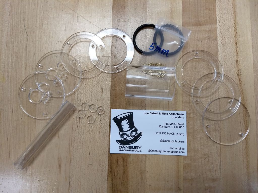
 I decided to make a new chamber because I need more space in the chamber that I can begin to build the electron detector. In the image above are the single parts of the chamber shown. The parts are made of 3mm acrylic sheet. The 5mm golden pogo pins are from Ebay and the black rubber rings are from sealing kit from Amazon.
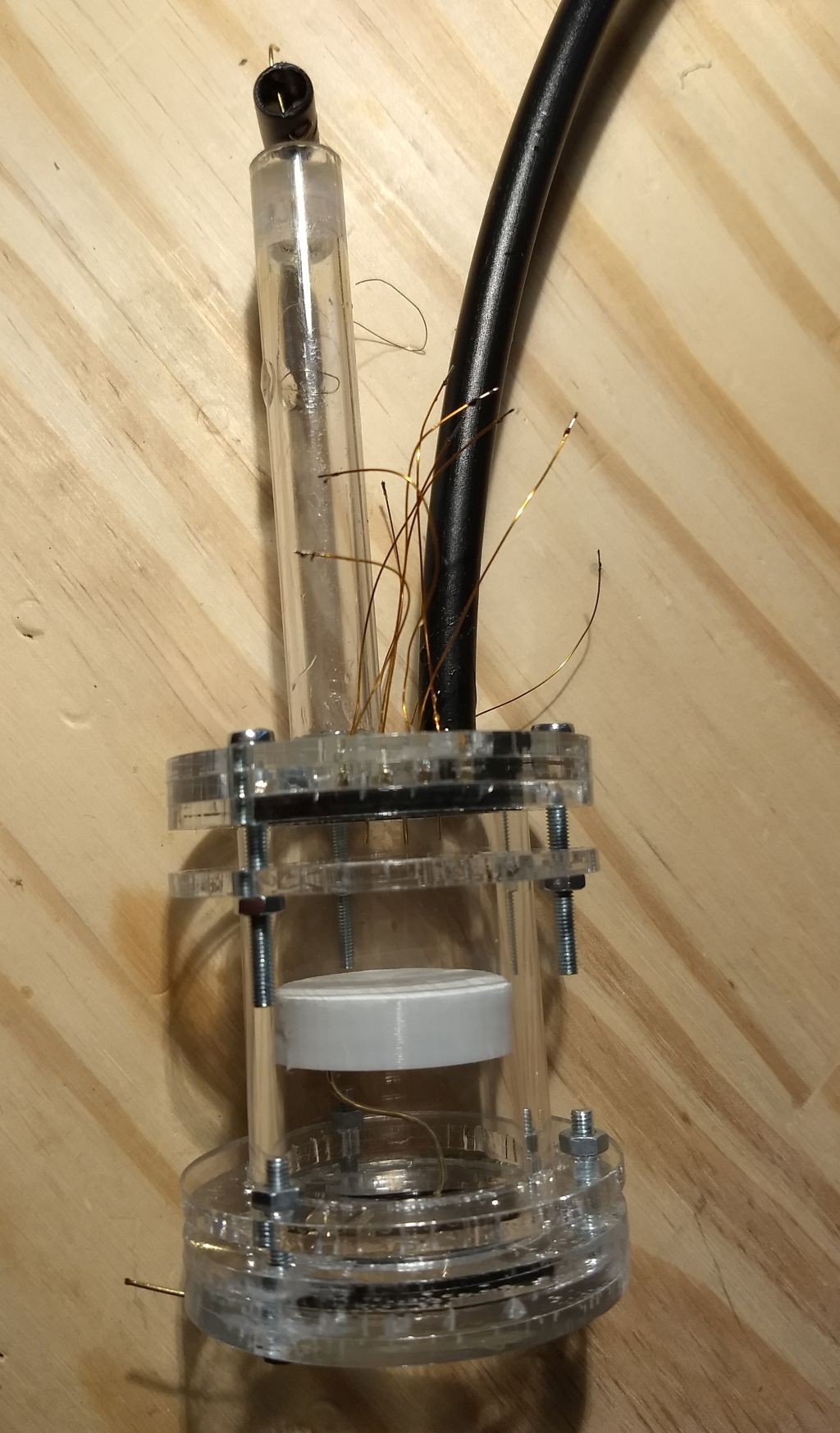
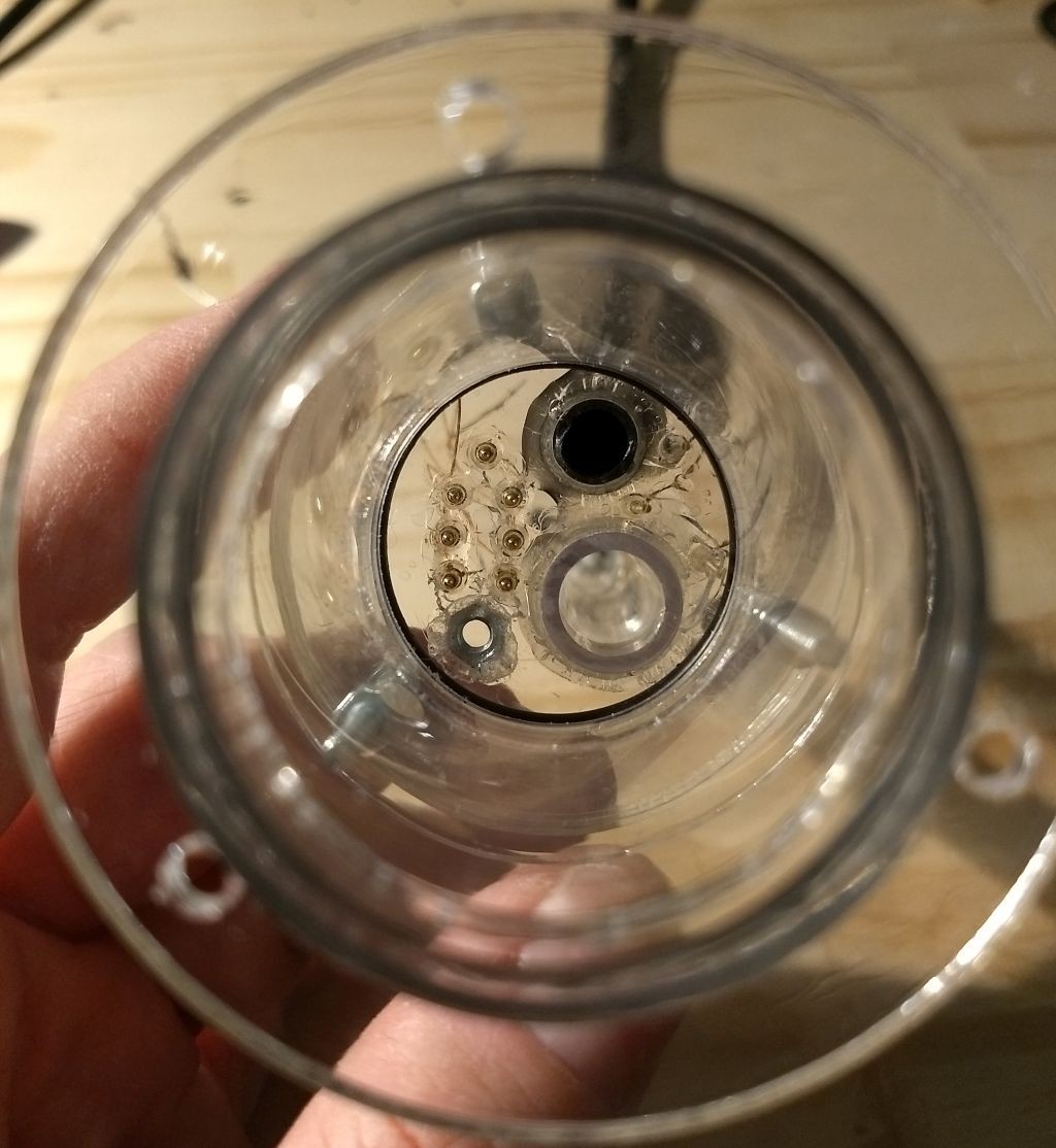
In the Image above are the assembled chamber shown. The white round disk in the chamber is a Zinc Sulfide screen to visualize the electron beam. On the image above are the connections in side the chamber shown. The black tube is the connection to the vacuum pump. The clear tube below is the entrance for the electron beam. Left to the tubes are the pogo pins and a nut. These elements should connect the electron detector to the outside. On right side are three pegs visible. With these pegs I want to measure the vacuum because I had a lot of trouble with the vacuum in the past.
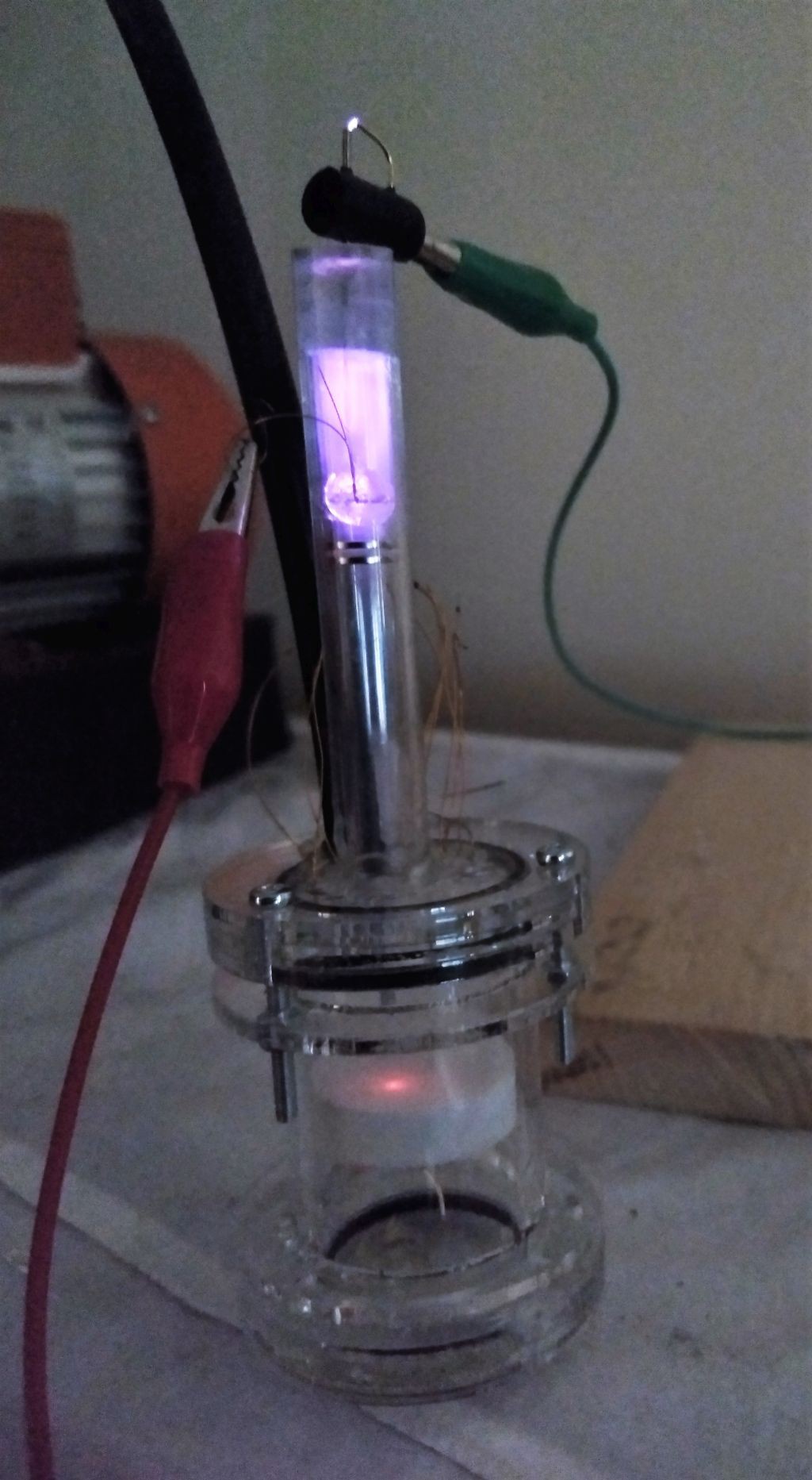
On the image above is electron beam in the chamber made of acrylic plastic shown.
-
STM32 Hello World
12/15/2017 at 21:10 • 0 comments
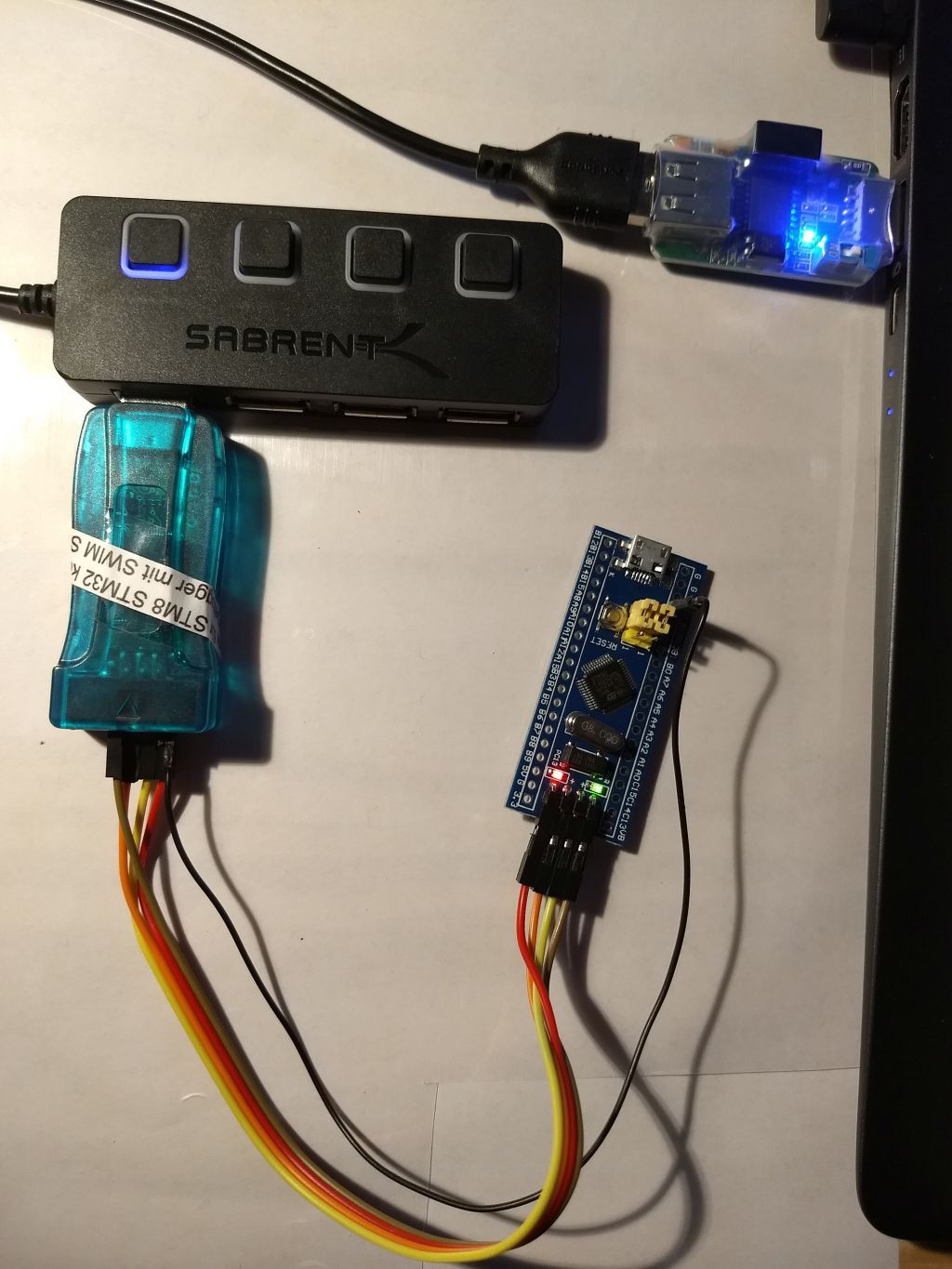
I started with the microcontroller. I programmed already several, but it is still the same. Its a pain in the neck until the tool chain is running and the "Hello World" led is blinking. I decided to use a STM32F103C8 because of the high clock frequency 72MHz and the 32Bit architecture. On the image above is my setup shown. Between the PC and the hub is USB isolatora from Ebay. Just for the case of something goes very wrong to protect my PC. The hub has the nice buttons to turn off each USB connector. The blue USB programmer is a ST-Link V2 from Ebay too.

One remarkable thing is that you need a additional rest cable which wasn't delivered with the programmer.
As IDE I use the pre-configurated eclipse version from AC6 which is available for download at toolchain .
The video above shows how to use the USB of the STM32.
3d Printed Scanning Electron Microscope
The goal is to build a DIY Scanning Electron Microscope (DIY SEM) with commonly available materials
 Chris.deerleg