STM32103RET6 ARM Cortex (currently, if i can't make the ADC behave and the SPI SLAVE to work correctly then going to flip back to the SAM7, which would suck a lot. (which we ended up doing for this round) ) I have still continued the STM32 build using the F4.
Spartan 3CS350 ( I got a metric tonne of them on eBay for ridiculously cheap )
SSD1306 driven 128x64 0.96" monochrome OLED ( I also picked up some larger sized ones that look like they'll fit the layout)
SDCARD
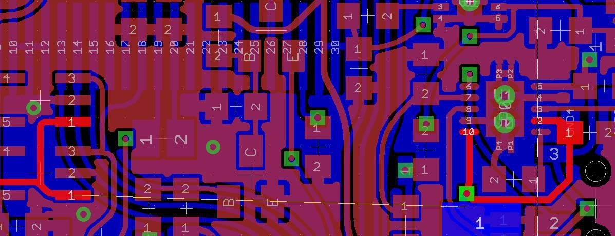
PCB Schematic Eagle 6, currently two layer, but we may go to four layer depending on ADC noise ( and cost )
HF 13.56Mhz and LF kHz reader, writer, cloning, decoding , investigating etc.
We may add a few "hidden" features to it as well.
rev3 has all the hardware SPI's in use, and a jumper to select ADC's so we can see if the extra voltage is to related to the shared pin. Moved everything around..
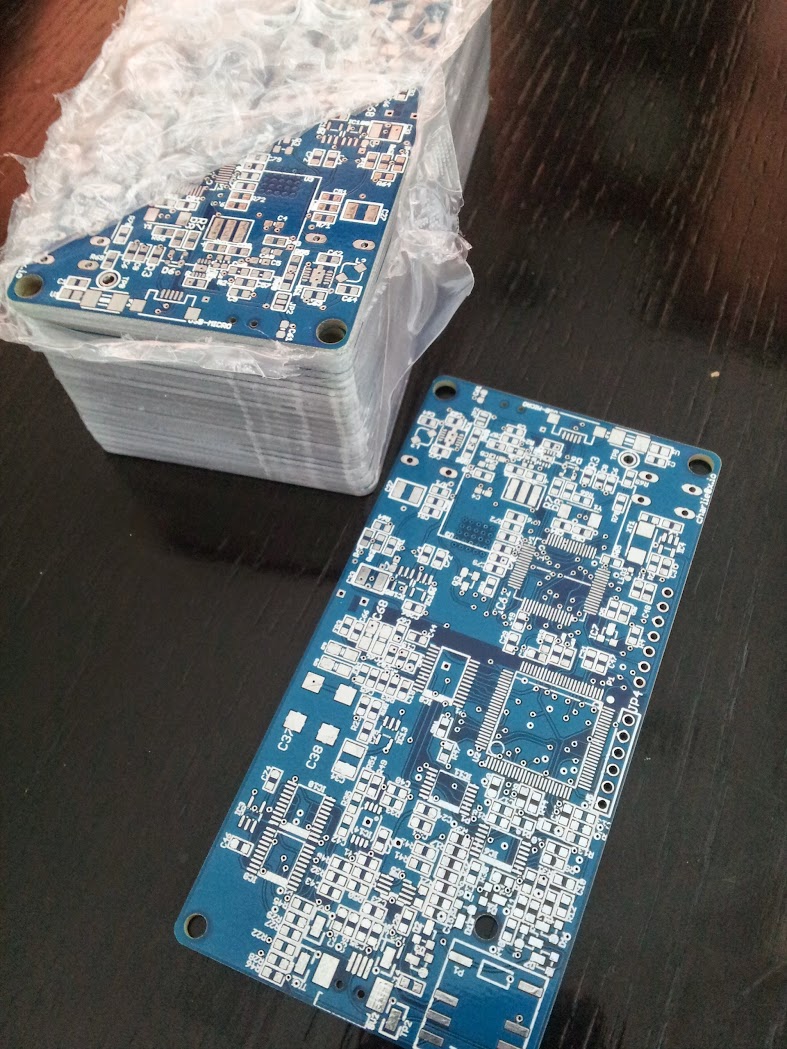
rev3 is a two layer, because well frankly i had issues routing it i thought it couldn't be done and have reasonable paths (See rev2) but i decided to rip * it all and redo it and i got it routed and still decent signal paths. The rev4 will be a four layer though, as we want to keep the noise down to a minimum. it'll add about $200 - $300 for the PCB's alone though !
There are a number of clocks on the board and analogue paths, so cross-talk / noise is an issue.
I dropped the IC based "relay" since it wouldn't handle the odd voltages the RF section can generate, but i found a suitable pin compatible replacement for the standard proxmark and also the OEM's replacement which is a different pin out (of course)
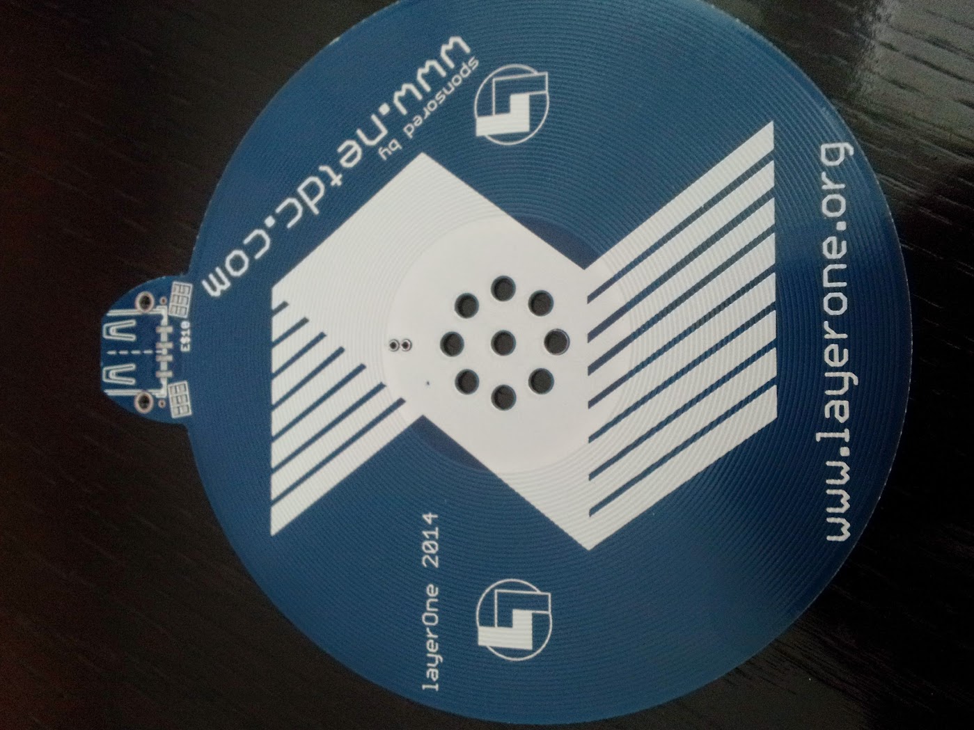
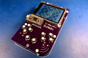
This is the first layerOne badge that has actually been rev'd!
Just to clarify, I did modify my SAMICE a tad.. so if you have one, you will not be able to use it for the badge :( since it won't work on non Atmel chips. I will bring a few ARM JTAG's though.
The latest board is using the AT91SAM7512B rev chip, we just didn't get some parts working in a time where I felt comfortable having the badge ready for conference day, i'm still keeping the STM32 F4 version alive though, its been routed and has been made,. I'm going to cut the traces on the rev3 STM32 F1 board and add the two caps that are needed for the later chips.
Also the SSP in the AT91 is pretty amazing, but expensive hard to get chip.
As a note to myself, its something i'll do in future, the only real changes on switching between those F1/2/3/4 CPU's are that there are two caps added on to two pins, so i'll always add the pads for them with jumpers prewired in the gerbers so that if i choose to go to a bigger CPU again, i can just cut the traces and add the caps.
I do like the STM32's but they do have a lot of problems that you have to do a lot of digging and reading on the forums to find, the only errata from ST seems to be "they're ok to use in gov stuff". Or you do what we did and try and see why doesn't this work ( hardware NCS/NSS being a big one) The data sheet is comprehensive and the STM32 library is nice too, but its only documented in the code, normally i'm ok with this since i'm usually of the mindset where if the code isn't readable enough to self document, its poorly written code, however in the case of low level hardware control its hard to tell whats going on all the time, especially if there are choices to be made, the people writing the data sheet are generally not the people writing the sample code/libraries. So there is often a disparity between naming conventions.
Things like speed selections, and pin modes ought to be documented , its great to have a library function that sets them, along with a whole bunch of asserts that check the modes ( but only atomically) but a few lines of comments saying what can be used, wouldn't go amiss. Some of this relies on the examples, but they don't cover all scenarios and its more of what you shouldn't do , versus should.
Once the PCB's are back and we've gotten the pressure of the build out of the way, i'll write up more detailed notes.
 charliex









 Piotr Esden-Tempski
 Just Me NL
 Antti Lukats
 stupid
SVN link is broken