-
Tested the EPM570 PCB version!
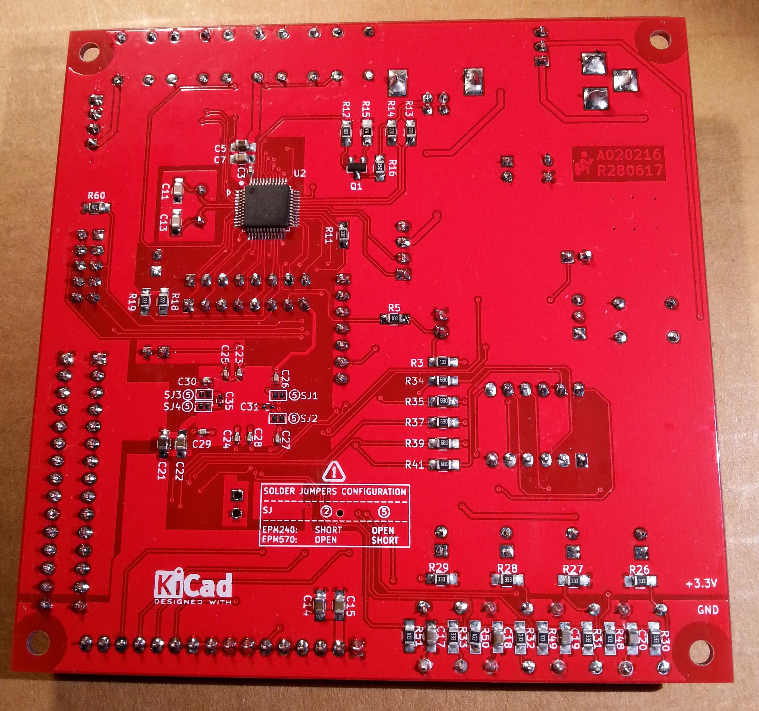
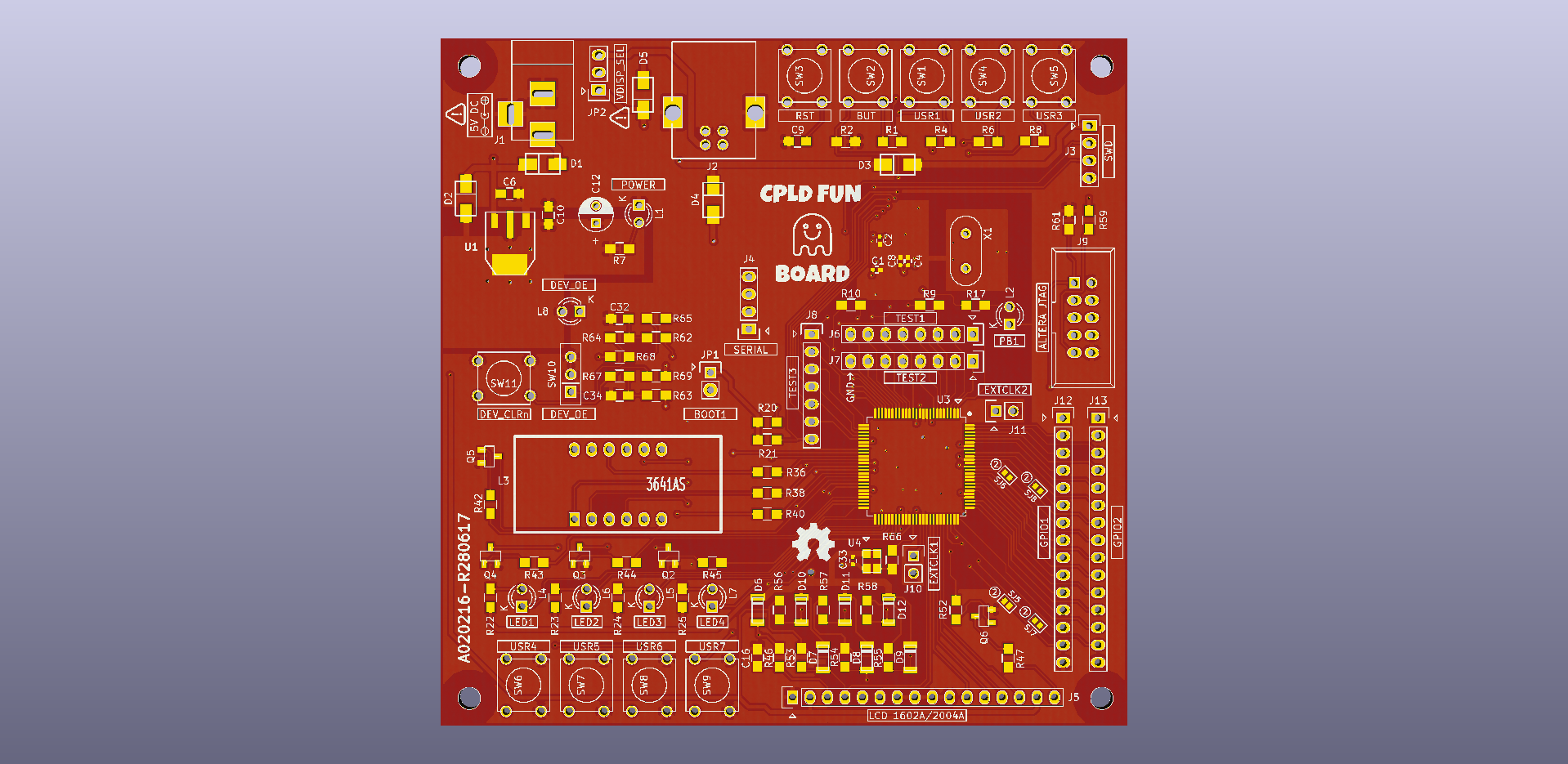
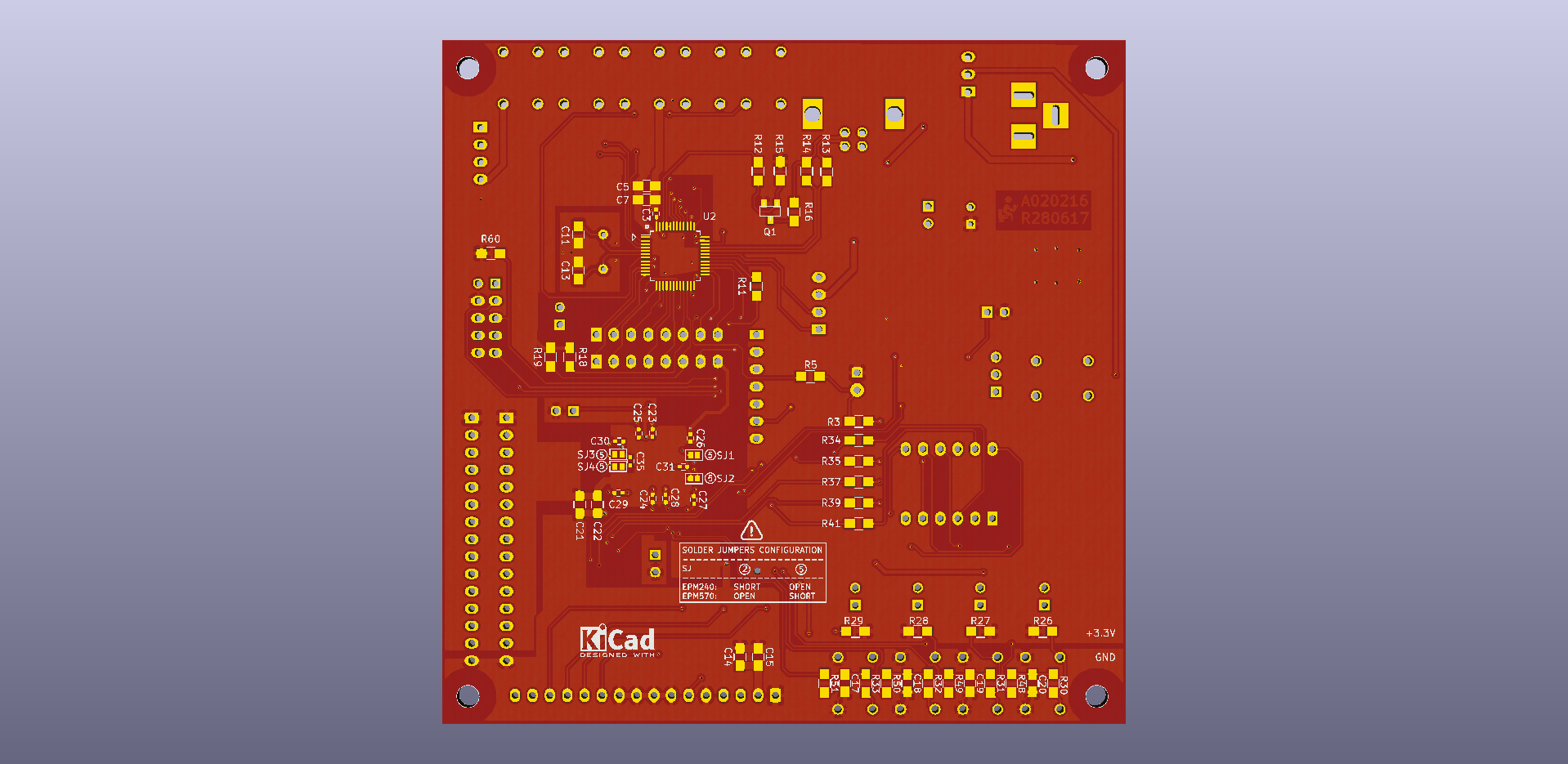
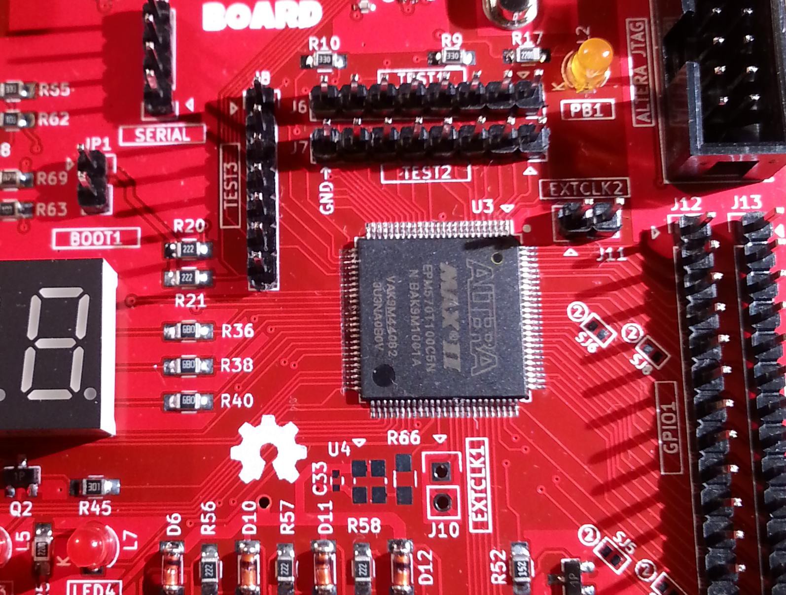
01/10/2018 at 16:02 • 0 commentsAt last I've assembled and tested the EPM570 PCB version:
![]()
![]()
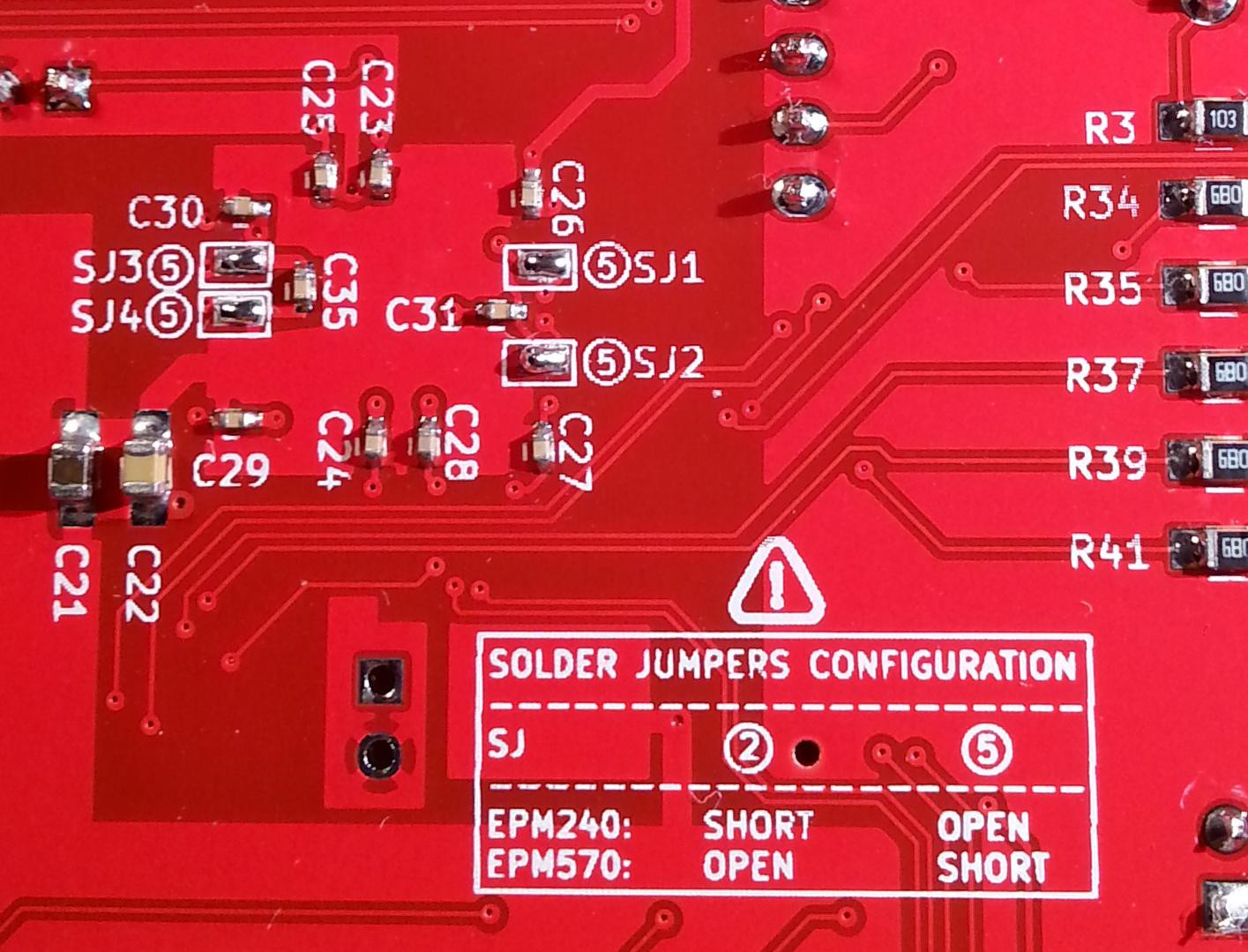
In the back of the PCB there is a short reminder about the solder jumpers you must use for the EPM570. In this case you need to populate C31 and C35 too (see the schematic).
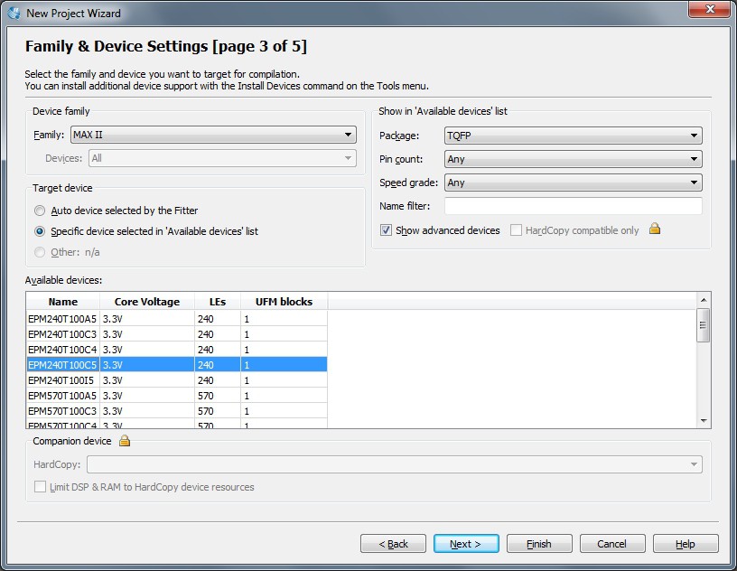
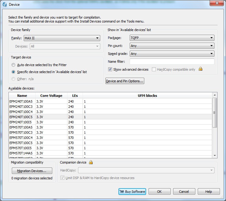
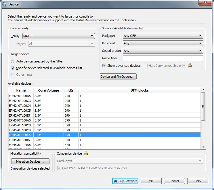
Of course in the Quartus II IDE you have to select an EPM570T100C5 as device too:
![]()
As an example here is the file: H051117_MultiFun_EPM570.zip. It is the complete Quartus II project for the EPM570 version described in the log: Multi-functional display/leds/keys custom controller. Project example.The sketch for the STM32 is (of course) the same used for the EPM240 version.
-
Multi-functional display/leds/keys custom controller. Project example
11/07/2017 at 07:29 • 0 commentsThis is a ready to use example of a custom "multi-functional" controller for a 4 digits 7-segments led display (single segment "graphic" drive mode with digits multiplexing), plus 4 status leds, plus 4 push buttons, using a bidirectional data bus (DATA_0-7) and a register selection bus (SEL_0-2). The command signals are an active low write signal (WR_EN) and an active low read signal (RD_EN). The behavior is very similar to a SRAM device.
To make things easier, in this example it is used the schematic editor and the 7400 devices family library, but note that this is not the best way to use a CPLD (the right way is to use VHDL/Verilog languages...).
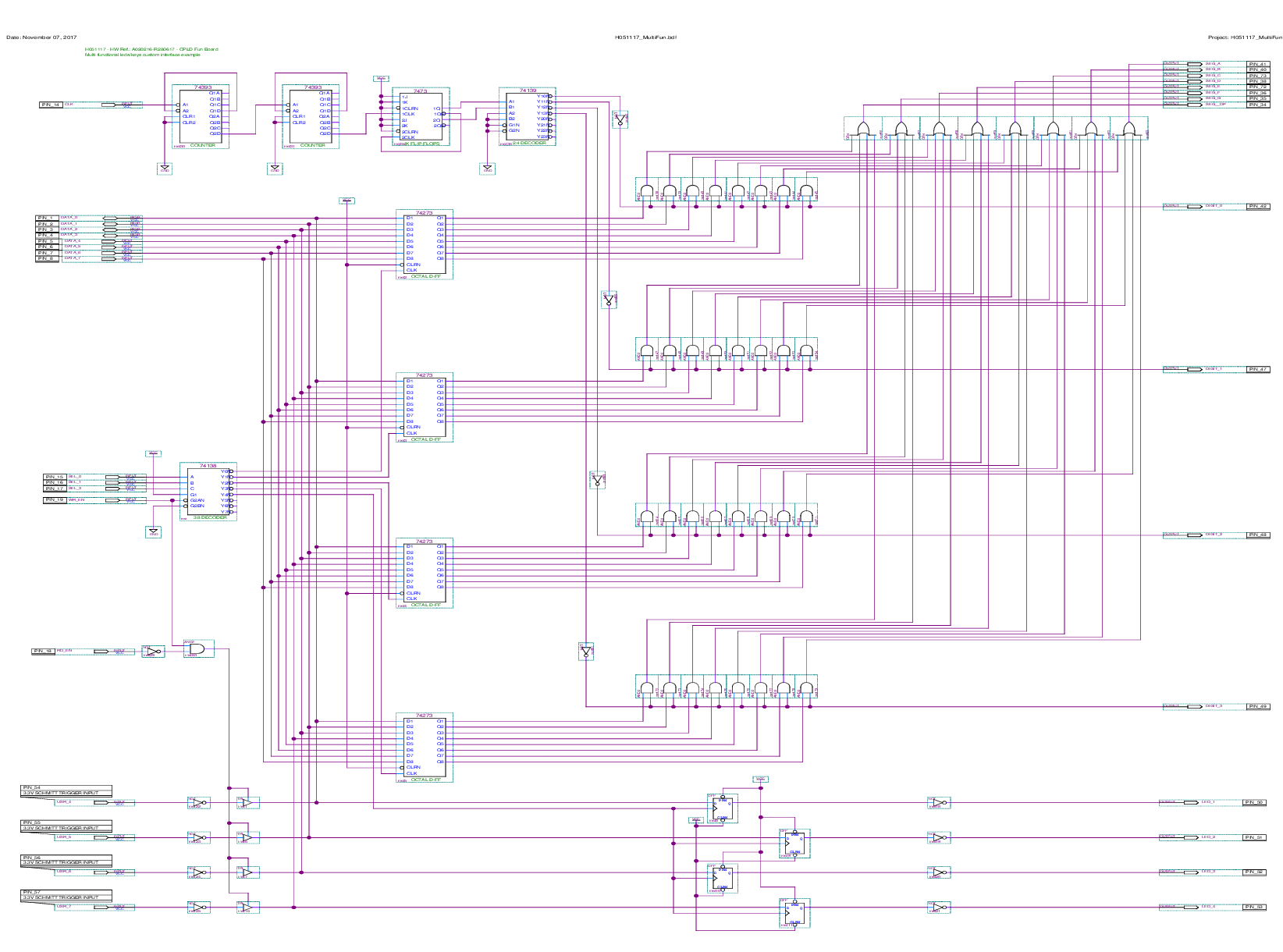
The schematic is the following (it is better use the Quartus II schematic editor to view it, opening the project):
![]()
The design is similar to the previous example. The input clock for the multiplex comes from the 36MHz clock (from the STM32 MCU), and is divided by two 1:256 dividers (74393).
The internal digit registers are now 8 bits wide, because now each single segment can be controlled (plus the "dot"), and there is a 4 bits register for the four leds LED1-4.
Only DATA_0-3 lines are really bidirectional, DATA_4-7 lines are not used in "read" mode and are tied to "1" using internal pull-up resistors.
A logic "1" in the DATA bits means "led turned on" or "push button pressed".
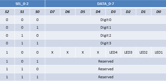
The "registers map" valid for the write operation is ("Reserved" means here "not used"):
![]()
where the generic "Digit n" byte used to turn on or off each single segment, is defined as:
![]()
This one is for the read operation (to check the four USR4-7 buttons status):
![]()
In the "read" mode there is no real register involved, so the SEL_0-2 lines are all "don't care".
The complete Quartus II project can be downloaded from this file: H051117_MultiFun.zip (the file is too big for this site, so it's stored externally).
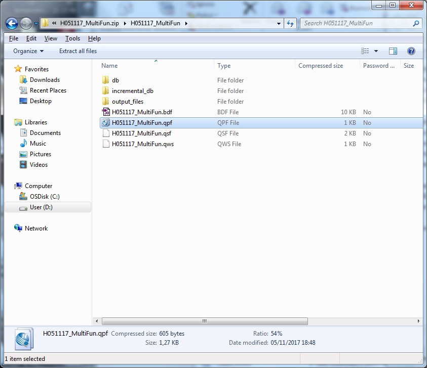
Unzip it taking its directory structure, and open it from the main Quartus II menu with "File" -> "Open Project..." selecting the file .qpf:
![]()
Upload the configuration into the CPLD as described in the Log: "Blink led example. Step by step guide".
WARNING: Because this is a bidirectional interface, take in account the considerations done in the "The DEV_OE switch and led" Log.
The sketch for the MCU side is S051117_MultiFun.ino (in the "Files" section) and must be uploaded using the Arduino IDE to run an application example.
The result is shown in this short video:The USR1-3 and BUT buttons are managed directly by the MCU.
-
Custom controller for a 7-segments display. Project example
11/02/2017 at 22:05 • 0 commentsThis is a ready to use example of a custom controller for a 4 digits 7-segments BCD led display.
To make things easier, in this example it is used the schematic editor and the 7400 devices family library, but note that this is not the best way to use a CPLD (the right way is to use VHDL/Verilog languages...).
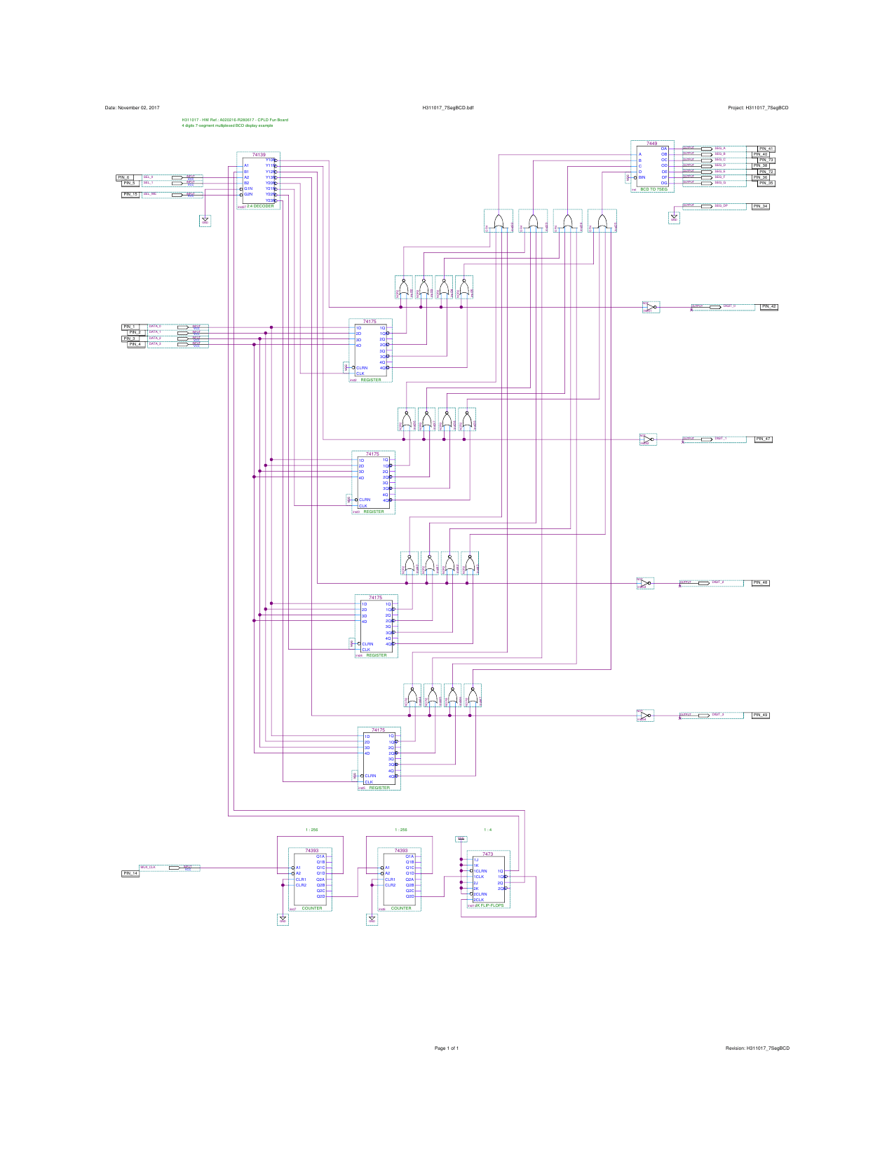
The custom controller has four registers (74175) to store the BCD digits, and drives a 4 digit BCD led display (already assembled on the board) with a BCD to 7-segments decoder (7449) using multiplexing. The input clock for the multiplex comes from the 36MHz clock (from the STM32 MCU), and is divided by two 1:256 dividers (74393).
The interface for the MCU is so composed:
- a 4 bits input data bus to receive a BCD digit (DATA_0-3);
- a 2 bits input address bus to address one of four digit registers (SEL_0-1);
- an input signal to write the digit to the selected digit register. The data and the address must be valid when the write signal is activated (SEL_WE).
Here it is the schematic of the controller configured inside the CPLD:
![]()
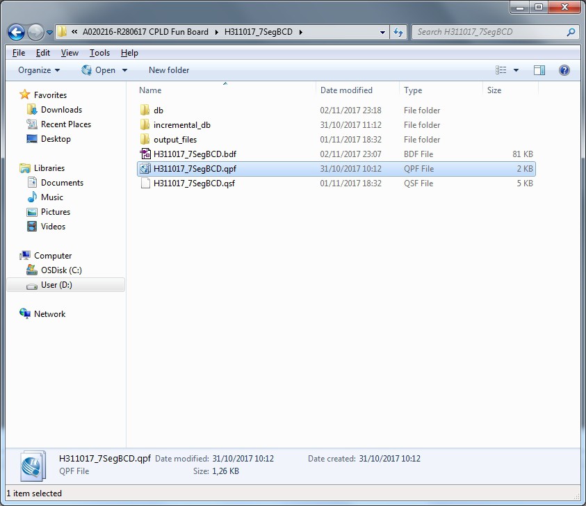
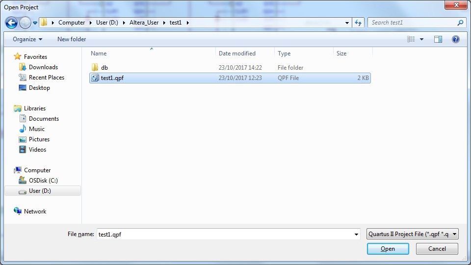
The complete Quartus II project can be downloaded from this file: H311017_7SegBCD.zip (the file is too big for this site, so it's stored externally).Unzip it taking its directory structure, and open it from the main Quartus II menu with "File" -> "Open Project..." selecting the file .qpf
![]()
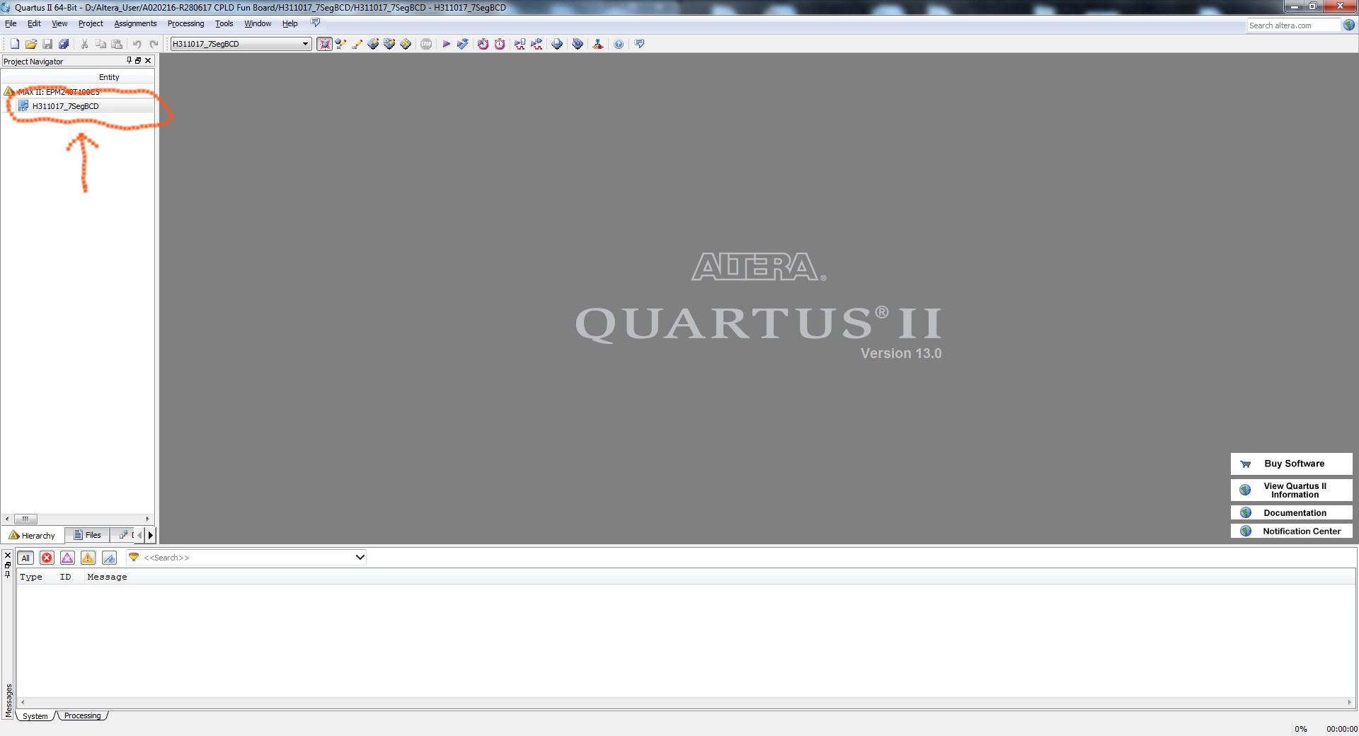
and double click on the file name to open the schematic editor:![]()
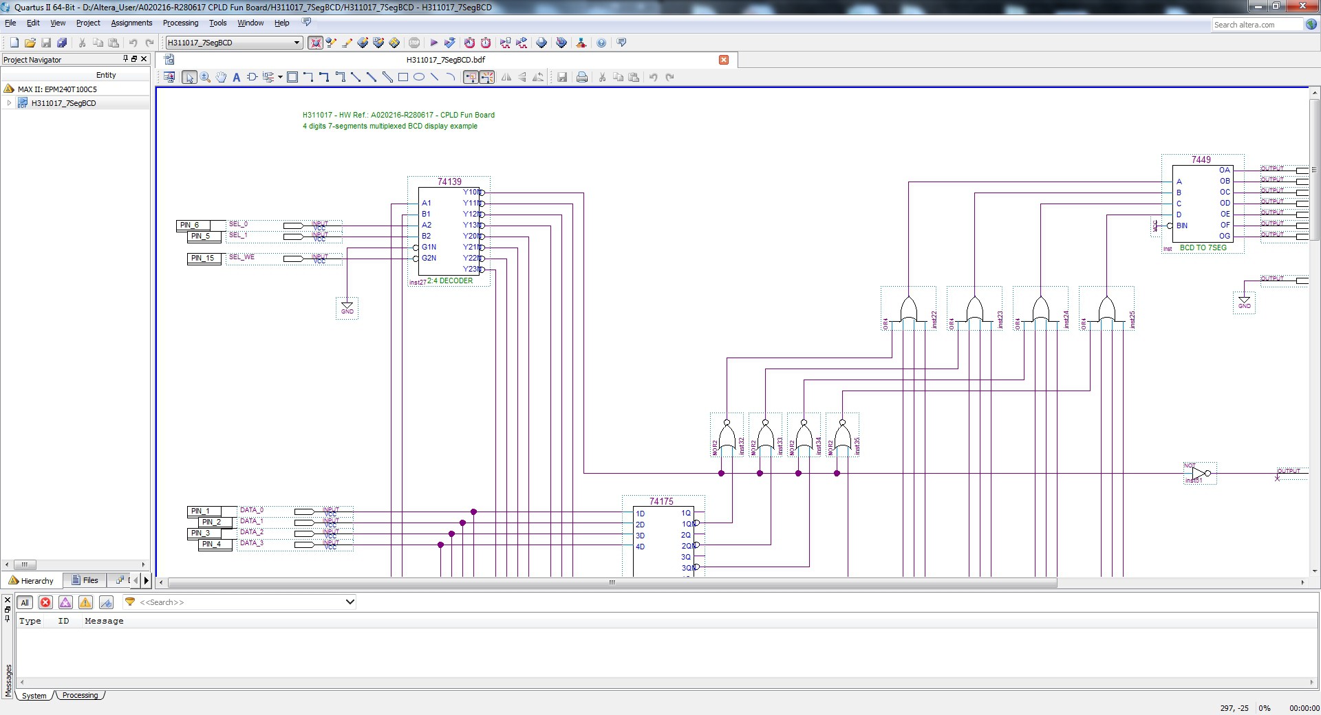
Here it is the schematic editor with the loaded project:
![]()
Now upload the configuration into the CPLD as described in the Log: "Blink led example. Step by step guide".
Then upload the sketch S311017_7SegBCD.ino (in the "Files" section) in the STM32 MCU using the Arduino IDE to run an application example using the custom interface.
The result is shown in this short video:
Note that pressing the DEV_CLRn button all the registers inside the CPLD are cleared.
-
The DEV_OE switch and led
10/30/2017 at 17:59 • 0 comments![]()
As already said in the previous Logs, the DEV_OE switch forces all the CPLD I/O pins into a HiZ state. When the DEV_OE switch is in the HiZ position, the DEV_OE led is on.
This switch comes handy in various way. A possible application is the case in which you want only use the STM32 "side" of the CPLD Fun Board, and use the TEST1-3 connectors as GPIOs pins of the MCU as a "Maple Mini" clone. In this way you can simply "freeze" the CPLD holding the configuration inside.
But there is a situation in which this switch comes very very handy. Imagine that you are testing a custom interface loaded into the CPLD, and simulating this interface in a "real" situation using the STM32 as "stimulus" generator. Imagine that you have some output pins (signals from the CPLD to the STM32) and some input pins (signals from the STM32 to the CPLD).
Now what it can happen if you want change, for any reason, an input as output and an output as input in the same change?
Well, if you update the CPLD configuration at first, the new configuration will change an input as output, so this can generate a short circuit between the CPLD and the STM32 because there would be two output connected together.
So you can decide to upload the new sketch at first with the new "scenario", but in this new sketch a STM32 pin will be changed as an output, so you have two output connected together too!
The only way to break this "deadlock" is to use the DEV_OE switch to force all the CPLD I/O pins to an HiZ state and then upload the new CPLD configuration and the new sketch for the STM32 with the input/output accordingly updated. Only when both CPLD and the STM32 are updated you can safely revert the CPLD from HiZ with the DEV_OE switch again.
Remember that the DEV_OE needs to be explicitly configured in Quartus II IDE (the DEV_OE LED will turn on also if not configured!), as explained in the Log: How to configure Quartus II. Step by step guide,
-
Blink led example. Step by step guide
10/24/2017 at 10:28 • 0 commentsCPLD configuration design (Quartus II)
Open yours previously saved project (see previous "Log") from Quartus II with "File" -> "Open Project..." and select the file "test1.qfp". The .qfp extension is used for the Quartus II projects:
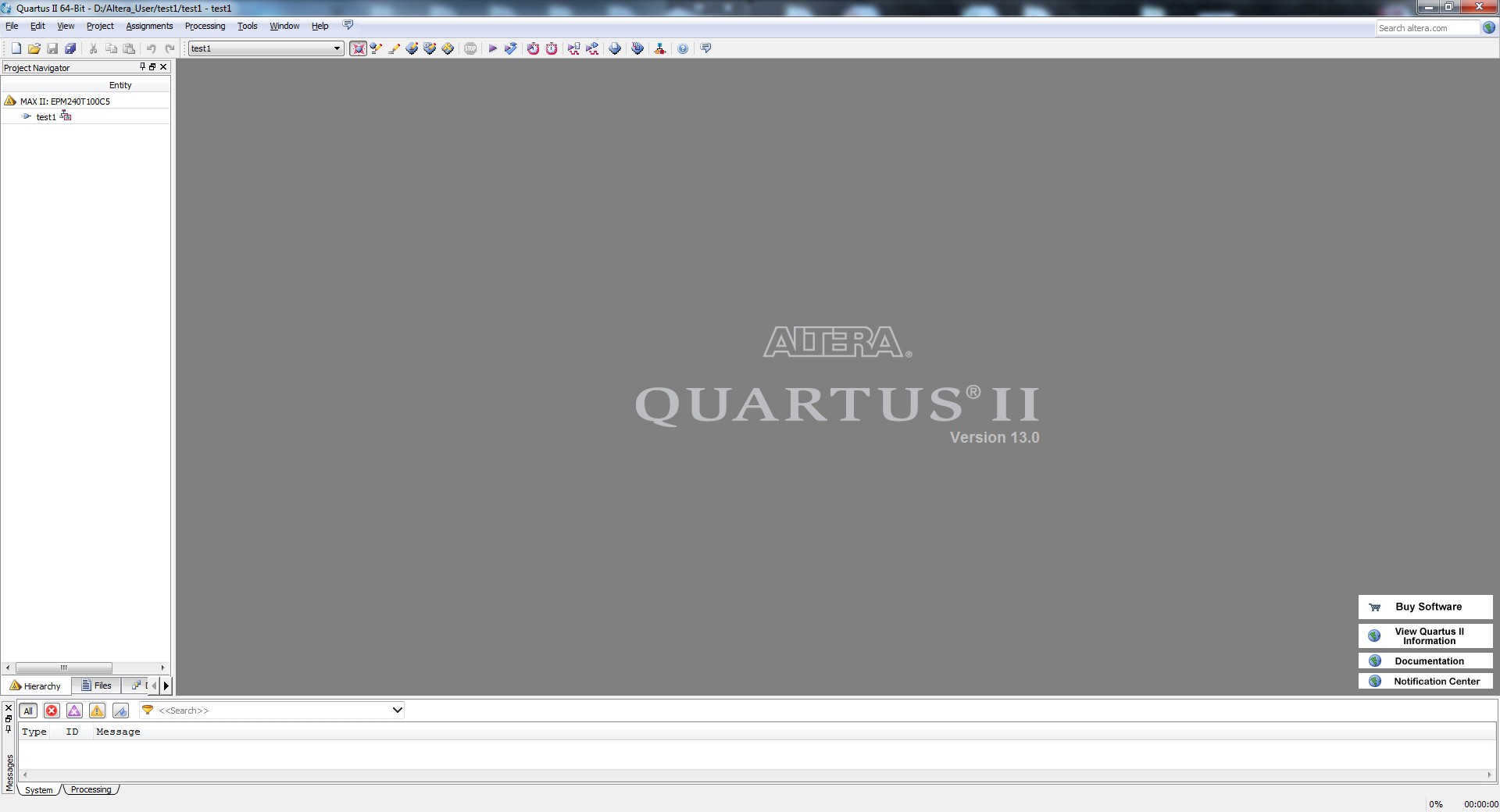
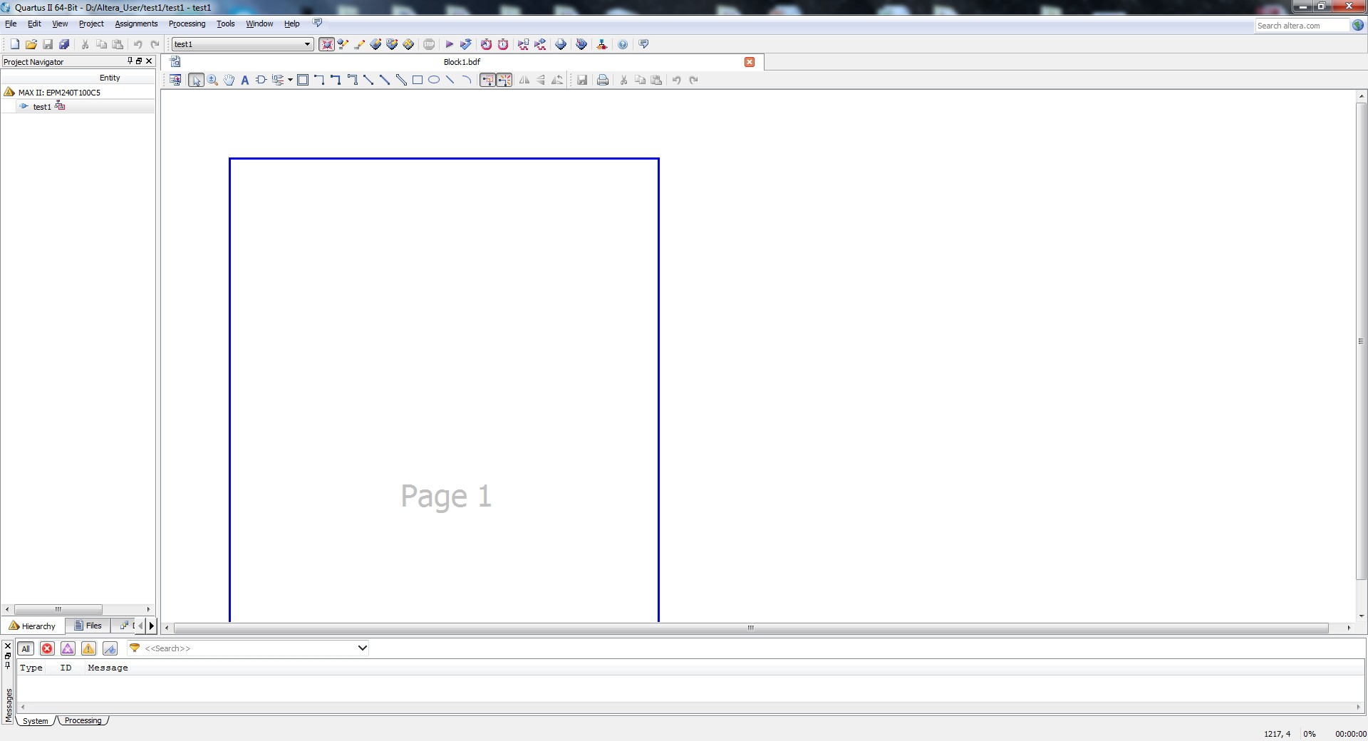
![]() This is the environment:
This is the environment:![]()
Now it is necessary to add a schematic sheet into the project.
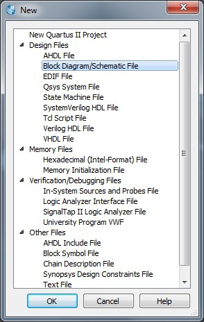
From the Quartus II menu click on "File" -> "New...":![]()
and select "Block Diagram/Schematic File". A new schematic file will be created:
![]()
Now it's time to design the needed circuitry to blink a led inside the CPLD.
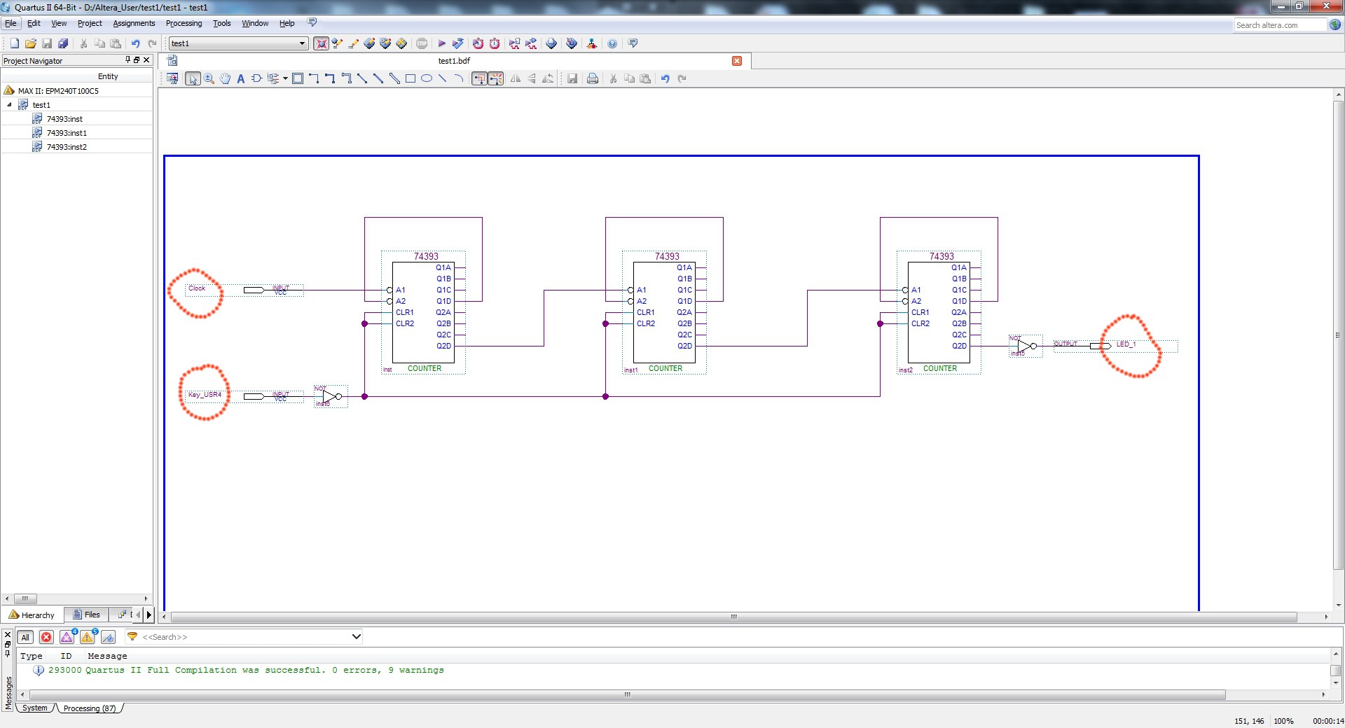
In this basic example, to make things easier, I'll use the schematic editor and the embedded library that emulate the well known 7400 device family to divide an input 36MHz clock till to about 2Hz. The 36MHz clock comes from the STM32 MCU using the STM32 MCO/PA8 pin (pin 29), that is connected to the CPLD GCLK1 (pin 14) pin . It will be possible see this signal using an oscilloscope connected to the pin 5 of J6 (TEST1 connector) and to the pin 8 of J7 for the GND (TEST2 connector).
Of course to create the 36MHz output clock from the MCU, a sketch must be uploaded into the STM32 flash using the Arduino IDE. In the following we will examine this sketch too.
Now I'll use three 74393 counters, each one connected to work as a 1:256 divider.
Form the designer tool bar select the "Symbol Tool":
![]()
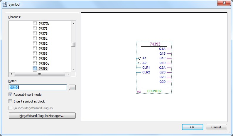
and then type 74393 in the "Name" field:
![]()
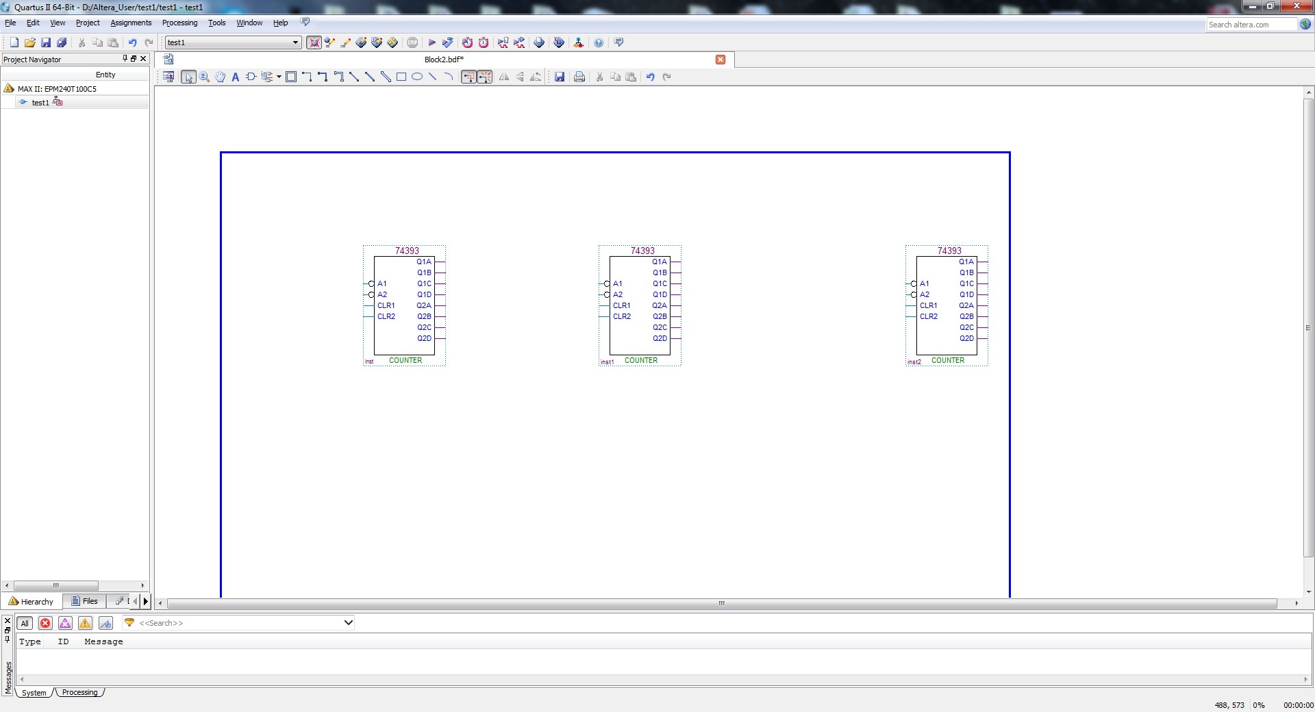
press the "OK" button and place three 74393 in the sheet (use the left mouse button to place):
![]()
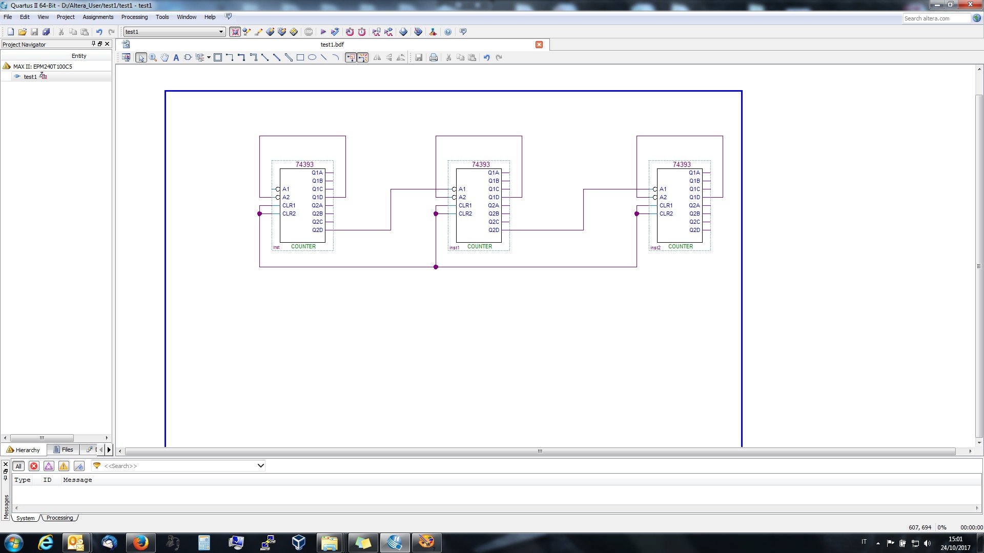
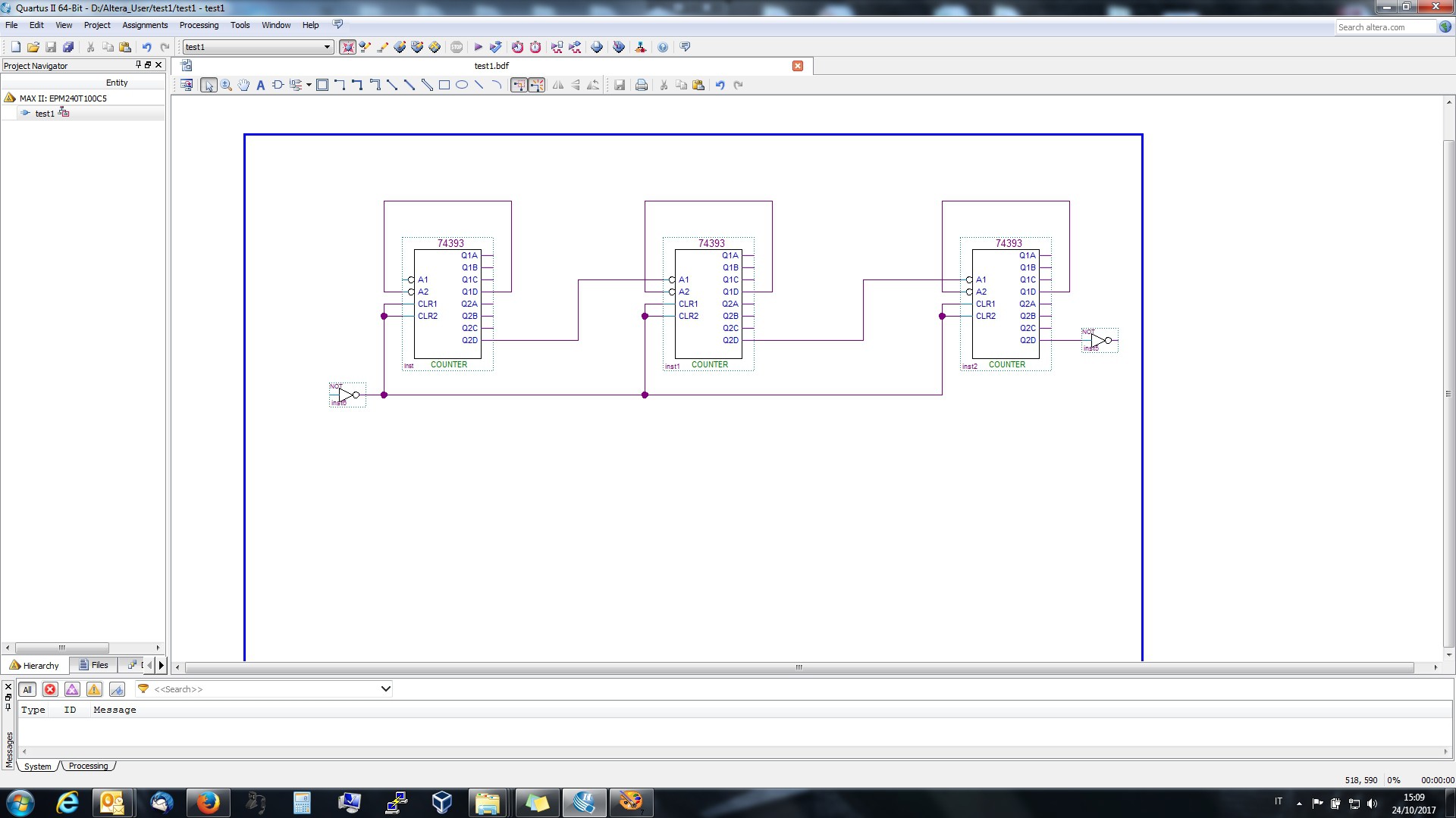
now press the "ESC" key and select the "Orthogonal Node Tool" to make connections:![]() and complete the connections as in the following photo:
and complete the connections as in the following photo:![]()
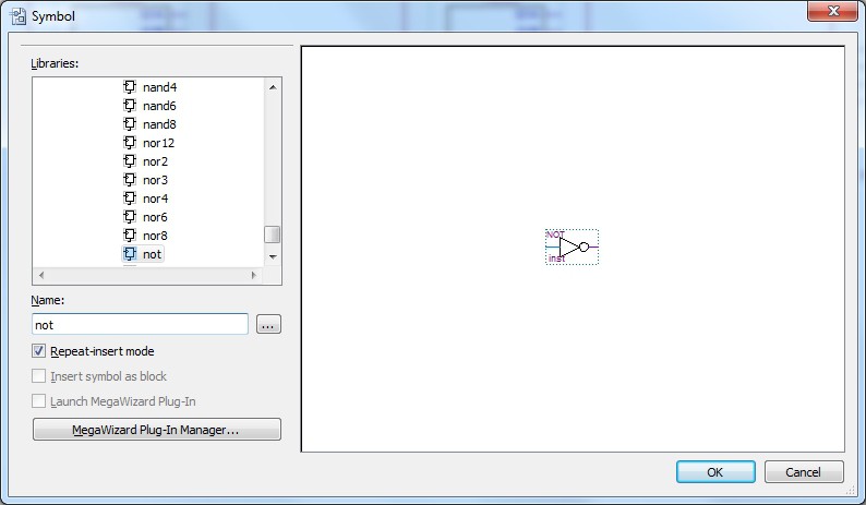
Now press the "ESC" key and select select the "Symbol Tool", then type "not" in the "Name" field:![]()
press the "OK" button and place two not in the sheet (use the left mouse button to place) and connect them as in the following:![]()
Now it's time to add the input (the input clock from the MCU) and the output (the led to blink). More, I'll add an input key to the Clear function common to the three counters.
So press the the "ESC" key and select select the "Pin Tool" and the "Input" sub-selection:
![]()
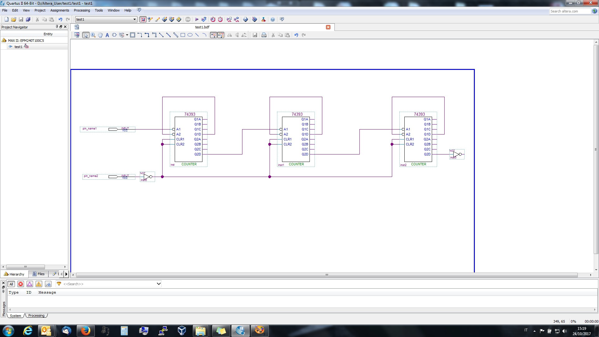
and place two input ports (as done before) and connect them as in the following photo:
![]()
Now I'll add an output port for the led.
Press the the "ESC" key and select select the "Pin Tool" and the "Output" sub-selection:
![]()
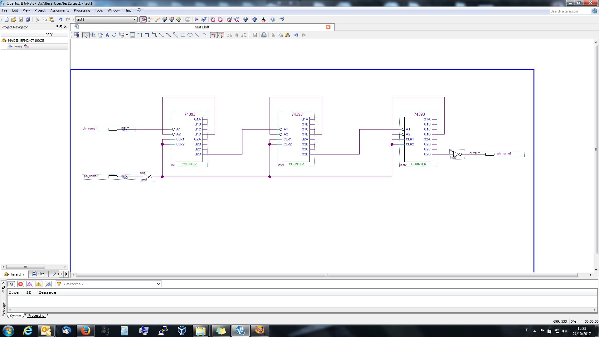
and place an output port (as done before) and connect it as in the following photo:![]() Now rename the names of the input/output pins (pin_name1, ...3) as in the following photo, clicking twice on each name:
Now rename the names of the input/output pins (pin_name1, ...3) as in the following photo, clicking twice on each name:![]()
Now the schematic entry is done, so save it.
The next step is the association of the input/output with real pins, and the definition of their electrical properties.
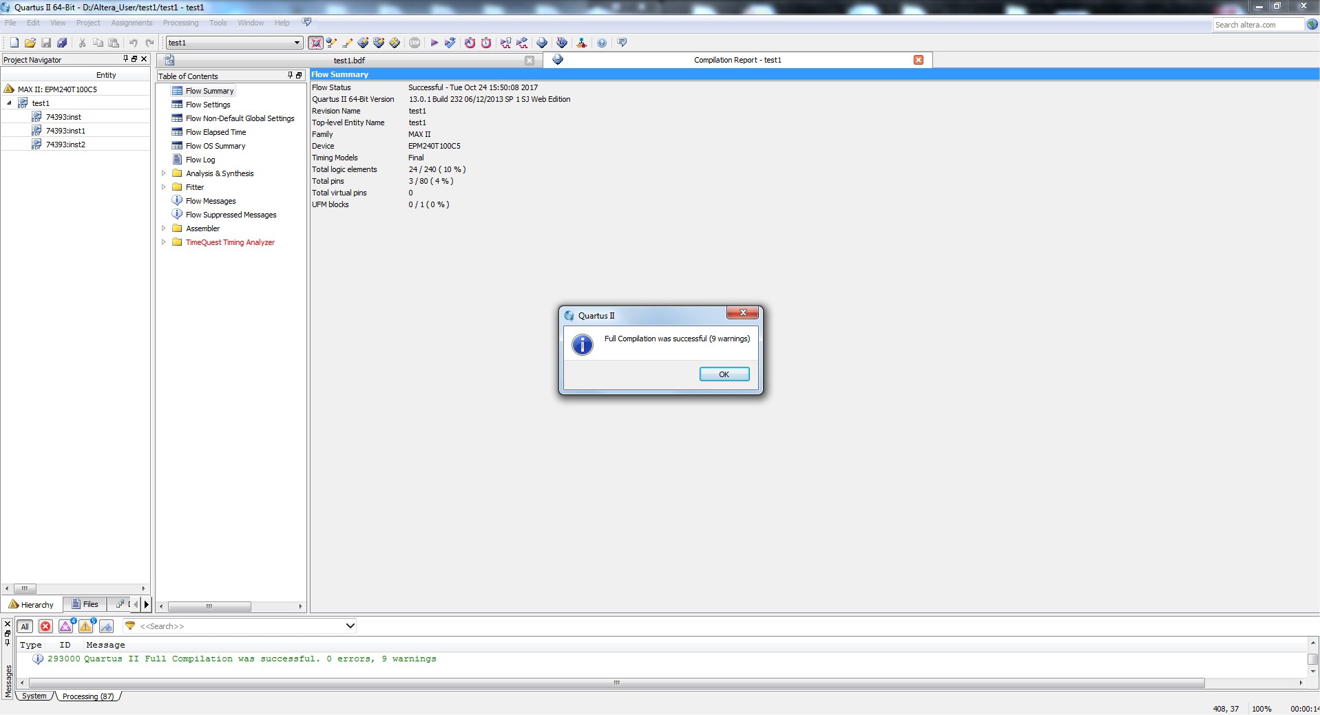
Before that it is convenient to do the compilation of the project, so press the "Compilation" icon:![]()
and wait the completion:![]()
Now press the "OK" button and then the "Pin Planner" icon:![]()
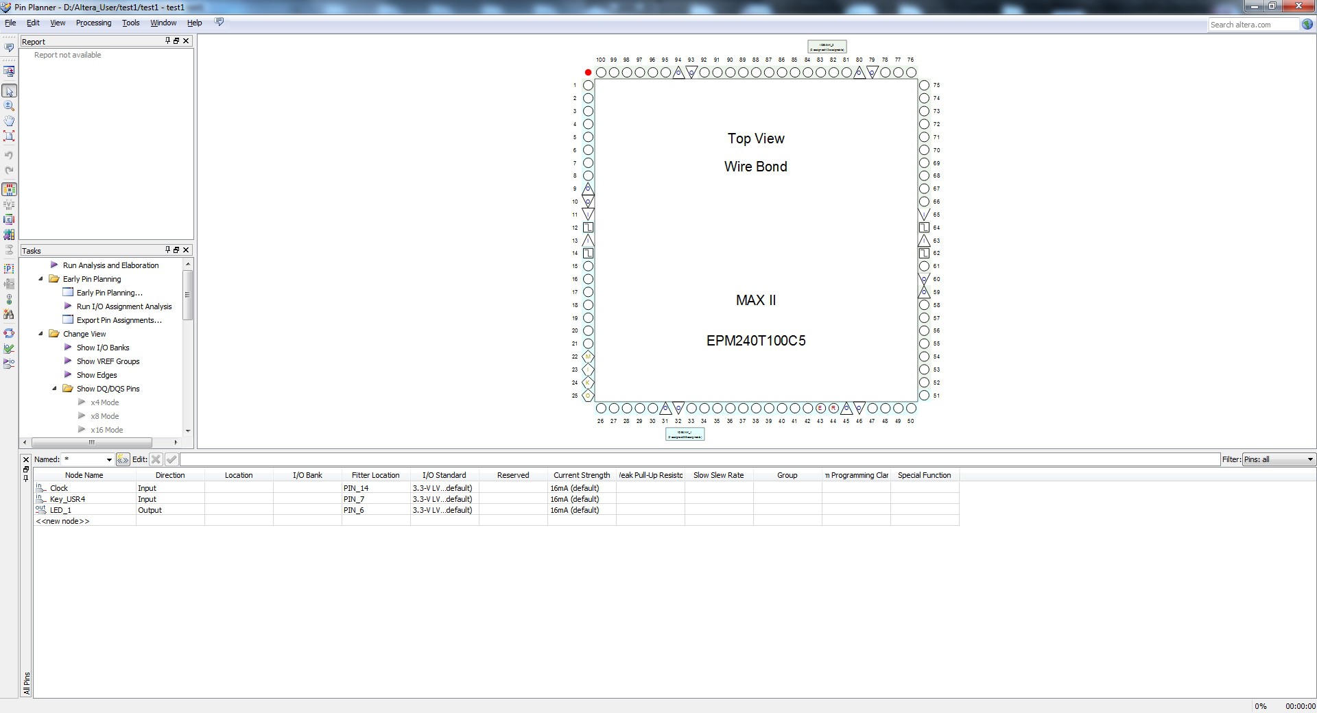
and the "Pin Planner" panel will be activated:![]()
This is the place where to define the CPD used pins and their electrical behavior (e.g. in this panel you can set the internal pull-ups, the maximum current, the digital levels, etc.).
Now set the correct physical pins in the "Location" fields in the bottom panel:![]()
To set the physical pins click on the "Location" field and select the pin to assign. Repeat this for every input/output pin (in this example there are three pins to assign). From the schematic it is possible check that the clock pin (from the STM32 MCO pin 29) is connected to the CPLD pin 14, the USR4 key is connected to the CPLD pin 54, and the LED_1 is connected to the CPLD pin 50. So edit the "Location" field accordingly.
After the editing, the configuration must be as in the following photo:![]()
Because the clock is made from the STM32, and in some conditions that pin can be in HiZ, it is better activate the pull-up resistor on pin 14 to avoid any floating state.
To do that click on the "Weak Pull-Up Resistor" and set it to "On":![]()
More, you must set the input behavior of the input pin 54 (connected to the key USR4) as a Schmitt trigger because there is a de-bouncing analog circuit on every key.
To do that change the "I/O standard" for that pin to "3.3V Schmitt Trigger Input" (note: if you don't see a column, right click on any column name and select the wanted column to the current view):![]()
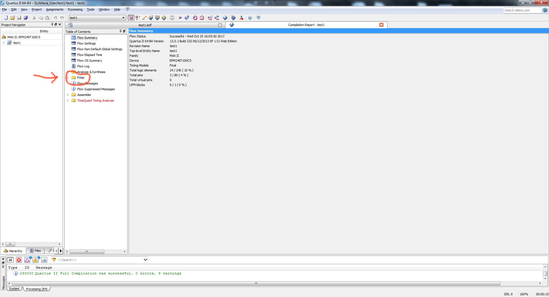
Now close the "Pin Planner" (no need to save anything here) and return to the main environment. From here compile the project again:![]()
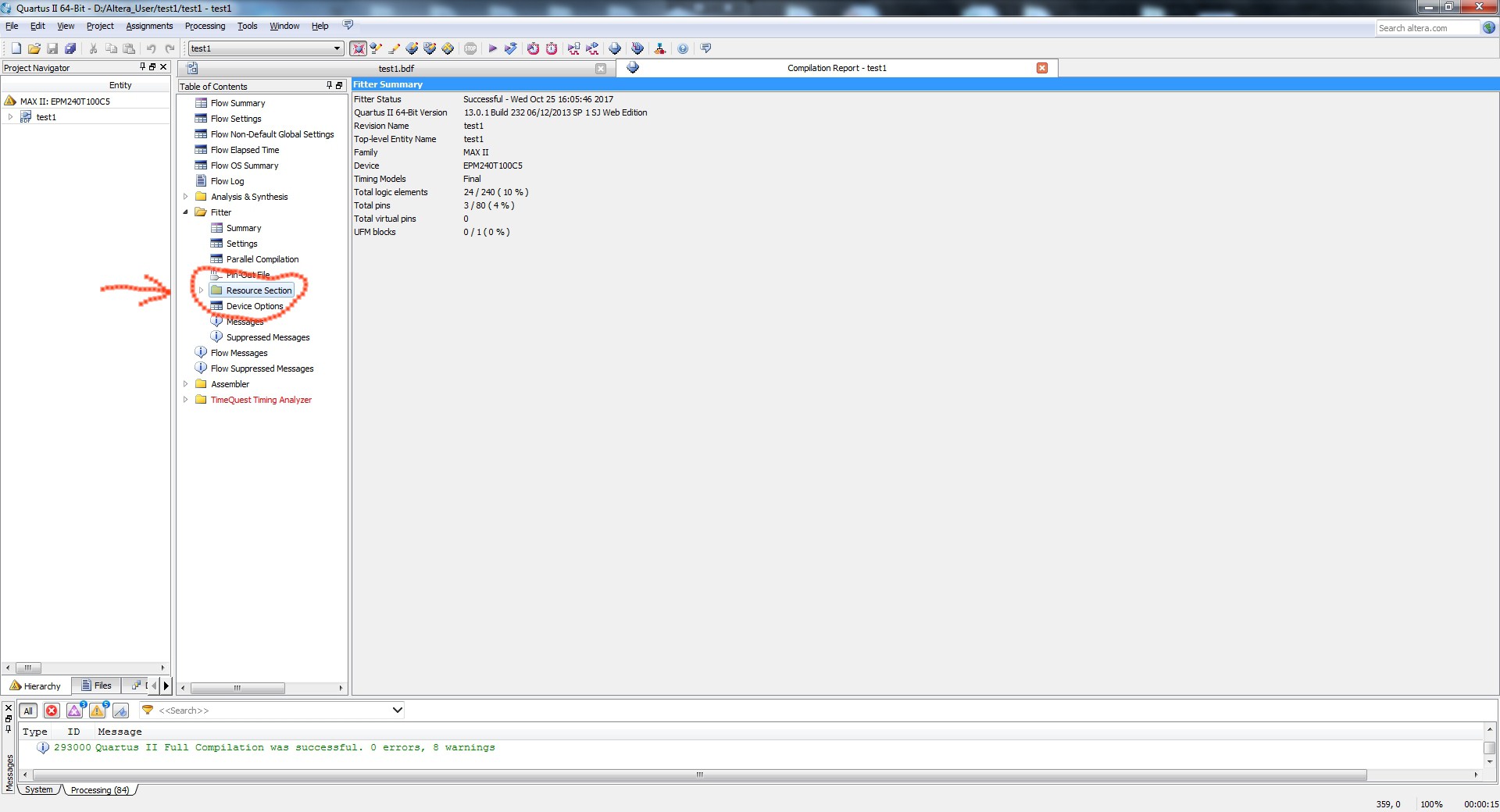
and check that all pins are set up as required. To do that go, soon after the compilation, click on the "Fitter" folder:![]()
and then clock on the "Resource selection" folder:![]()
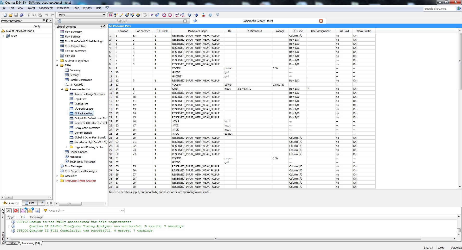
and on the "All Package Pins" element:![]()
and check that all the pins are configured as wanted.USB Blaster connection procedure
After that you are ready to upload the configuration into the CPLD.
To do that you must follow the suggested steps as described in the Usb Blaster User Guide:- Check that the target (the CPLD Fun Board) is not powered;
- Connect the Usb-Blaster programmer first to the Workstation USB;
- Connect the JTAG cable to the target;
- Power the target. This means connect the CPLD Fun Board USB connector to an other USB port on the Workstation.
Remember that the USB Blaster can't power the target. The power comes from the USB connector.
Here a short video about how to connect the USB Blaster dongle:
CPLD programming (Quartus II)Now click to the "Programmer" icon in the main window:
![]()
and the "Programmer" window will pup up:
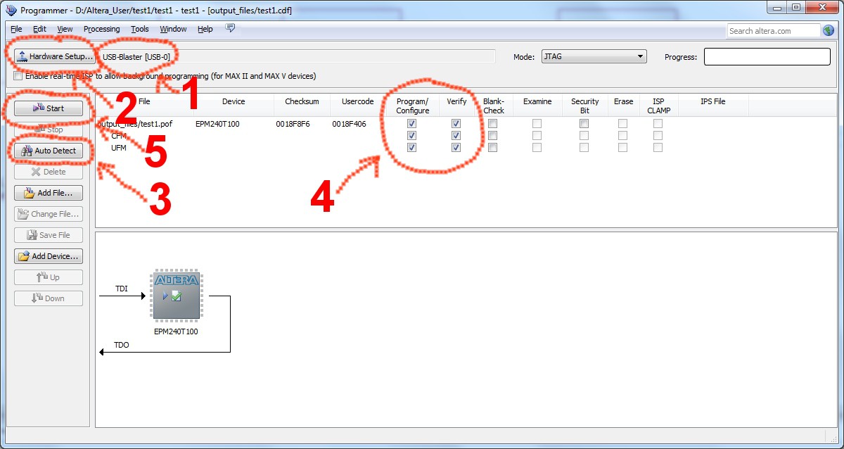
![]()
Now some check:
- Check if the "USB-Blaster" device is selected (1);
- If not, press the "Hardware Setup..." button and select it (2);
- Press the "Auto Detect" and you shouldn't see any error (3);
- Check all the "Program/Configure and "Verify" check boxes (4);
- Press the "Start" button to upload (5).
STM32 clock generation sketch (Arduino IDE)Now you must upload a "Sketch" in the STM32 with the Arduino IDE to generate the needed clock signal.
Copy the following code to a new sketch inside Arduino IDE:
void setup() {
  // put your setup code here, to run once:

  // Set the MCO pin to output the clock to the CPLD (GCLK1 pin 14). See STM32F103 Reference Manual RM0008
  RCC_BASE->CFGR =  RCC_BASE->CFGR | 0x07000000;    // Set MCO[2:0] = 111 (inside RCC_CFGR register) for 36MHz clock output
  GPIOA->regs->CRH = GPIOA->regs->CRH | 0x00000003; // Set output mode on PA8 @ max freq 50MHz (MODE8[1:0] = 11)
  GPIOA->regs->CRH = GPIOA->regs->CRH & 0xFFFFFFF3; // Set output mode on PA8 as general push-pull output (cnf8[1:0] = 00)
  GPIOA->regs->CRH = GPIOA->regs->CRH | 0x00000008; // Set output mode on PA8 as alternate push-pull output (cnf8[1:0] = 10)

}

void loop() {
  // put your main code here, to run repeatedly:

}
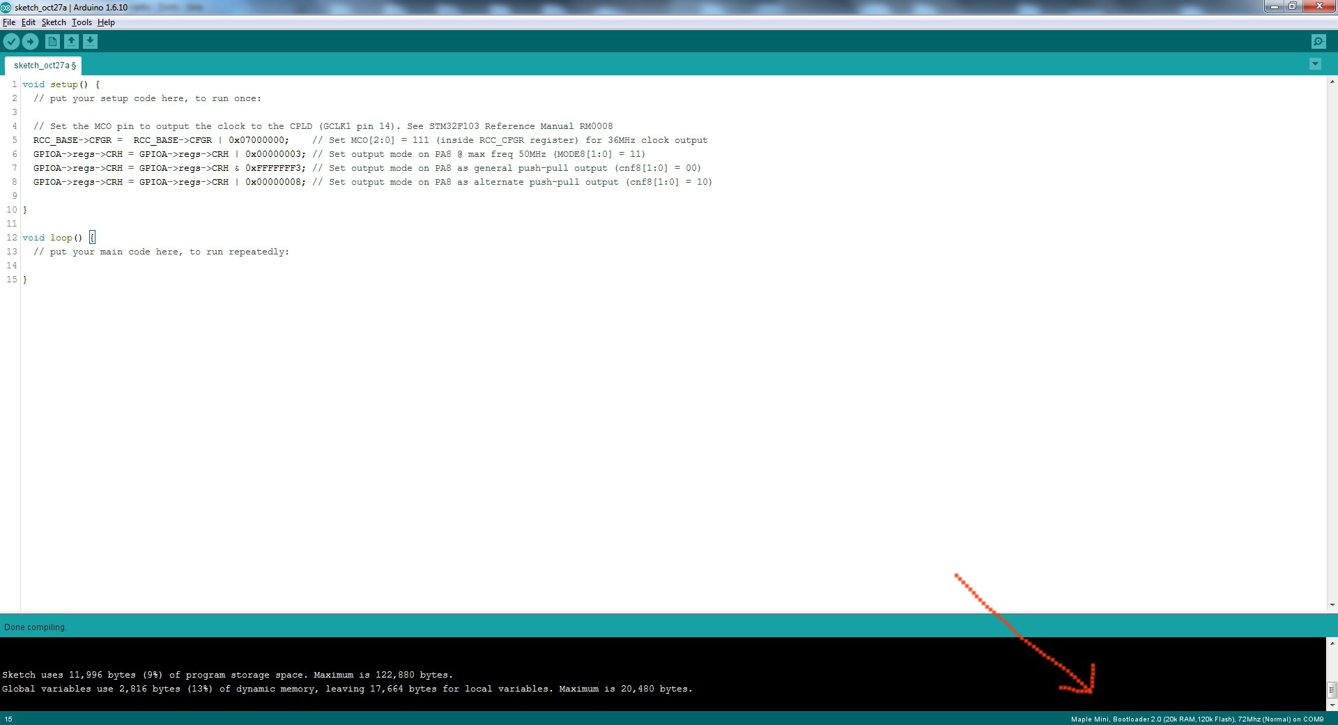
and upload it, but before check that the target board is a "Maple Mini" running at "72 MHz" and having a the "Bootloader 2.0":
![]()
After the upload LED1 will blink at about 2Hz. If not check that the DEV_OE led is off; if it is on turn it off using the DEV_OE switch.
Here is the result:
In the video you can see that when the RST button is pressed and the STM32 resets, the blink stop for a while. This because the clock is provided by the STM32.
You can see the effect of the DEV_CLRn button that reset all the FFs inside the CPLD making the counter stop. Same behavior pressing the USR4 button connected with the Clear signal of all configured counters.
Switching the DEV_OE all the CPLD I/O pin go in HiZ, so no blinking again.
Of course the DEV_CLRn and DEV_OE have effect only if you have previously checked them in the Quartus II setting windows.
USB Blaster disconnection procedureNow, to disconnect the USB Blaster dongle you must follow the suggested steps as described in the Usb Blaster User Guide:
- Power off the target. This means disconnect the CPLD Fun Board USB cable;
- Disconnect the JTAG cable from the target;
- Disconnect the Usb-Blaster programmer from the Workstation USB.
Here a short video about how to disconnect the USB Blaster dongle:
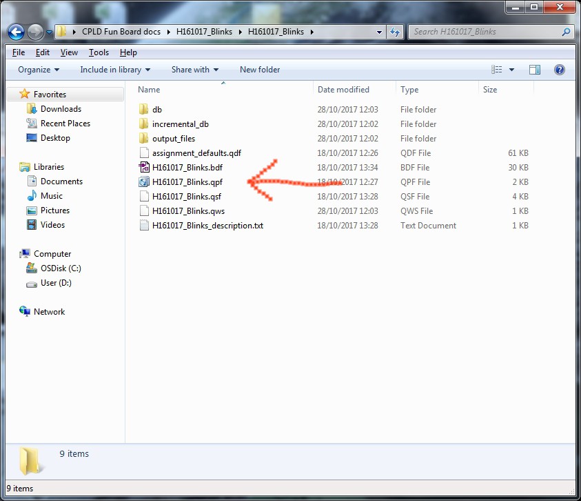
An example ready to useI've made a blink example ready to use. In this example it is used the schematic editor, but note that this is not the best way to use this devices (the right way is to use VHDL/Verilog languages...). Download the file H161017_Blinks.zip (the file is too big for this site, so it's stored externally) and unzip it taking its directory structure. This is a complete Quartus II project, so you can open it from the main menu with "File" -> "Open Project..." selecting the file .qpf inside the downloaded zip file:
![]()
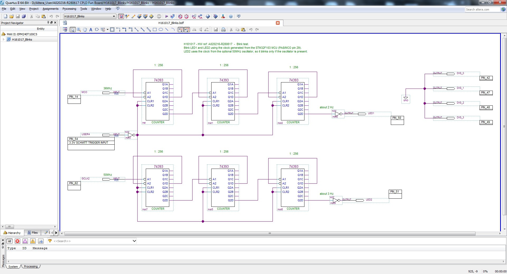
It is a blink led example similar to the previous, but with an other series of divider connected to the optional 50MHz oscillator. If populated it will blink the LED2 too:
![]()
More, the four outputs (DIG_0-3) that drive the common pin of the four digit of the 7-segment on-board led display (see the schematic) are tied to GND to avoid the flow of a low drive current from the internal pull-up resistors due to the default configuration for all the unused I/O pins (HiZ with pull-ups enabled). This current is the cause of the very low light that you can see from the led display in the previous CPLD configuration.
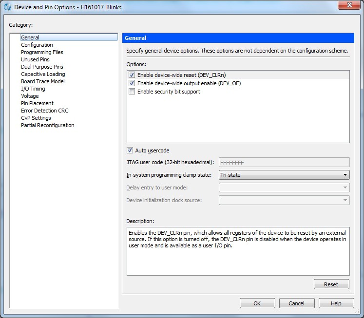
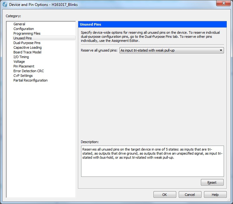
Remember to verify always the "general device pin options":
![]()
and the "unused pins" option:
![]()
as described in the previous example, and in general all the others settings.
The sketch to use for the STM32 is in the "File" section: S161017_BlinkTest.ino.
This sketch will generate the 36MHz clock to blink LED1, and will blink the LED_PB1 led connect to the STM32 too (see inside the code of the sketch).
The following video shows the result:Both the boards have the same CPLD configuration and the same sketch on the STM32 MCU.
The board on the right (it is a previous PCB revision) has the 50MHz oscillator populated.
You can see that pressing the RST button (STM32 reset) the LED1 stops to blink for a while because the STM32 stops to generate the clock, but LED2 on the right board continues to blink because the clock comes from to the 50MHz optional oscillation (see the schematic).
The DEV_CLRn button stops both LED1 and LED2 blinking because forces all the FFs of all the LEs (Logic Elements) inside the CPLD to reset (until it is released), instead the LED_PB1 is unaffected because driven by the MCU.
-
How to configure Quartus II. Step by step guide
10/23/2017 at 10:15 • 0 commentsIn the following I'll use Quartus II version 13.0SP1 (Service Pack 1) because for an other project I need the compatibility with the Cyclone II FPGA series (this version is the must updated that supports those), and it is related to the EPM240T100 "flavor" of the CPLD Fun Board.
After installing Quartus II IDE (you can get it from here after a registration) it is necessary change some default setting to better suit the CPLD Fun Board.
This setting must be used for every new project, so in the following we'll see how to create a new project and apply the correct setting.
From the Quartus II menu select "File" -> "New Project Wizard..."
![]()
Click "Next >"
![]()
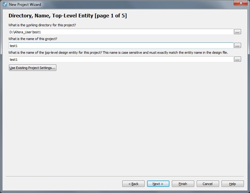
Fill the directory for the new project, and the others names. I suggest to use the same name for all the fields (as done in the photo). Remember to avoid names with spaces inside! Then click "Next >" again
![]()
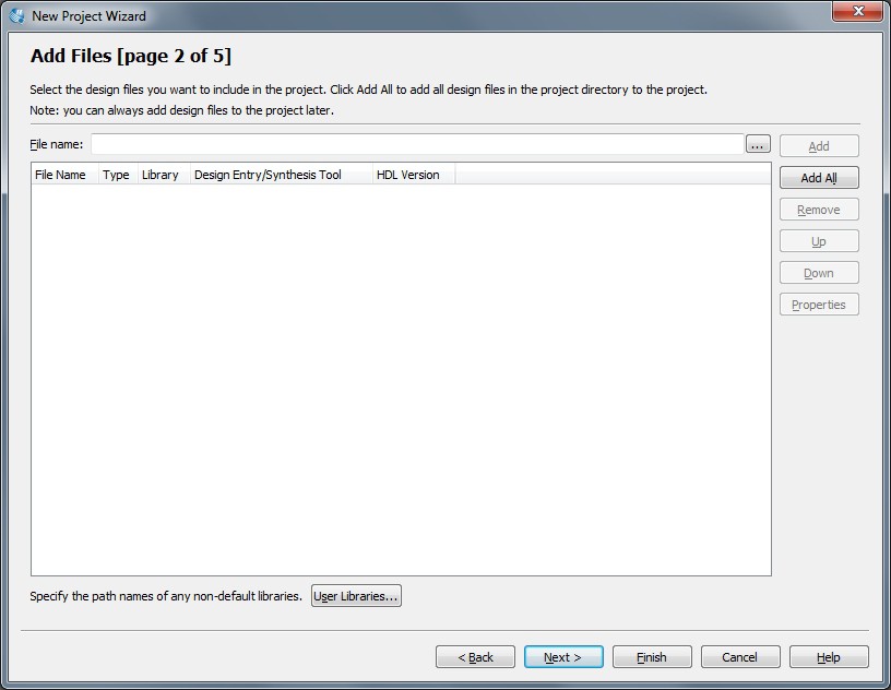
click "Next >" again
![]()
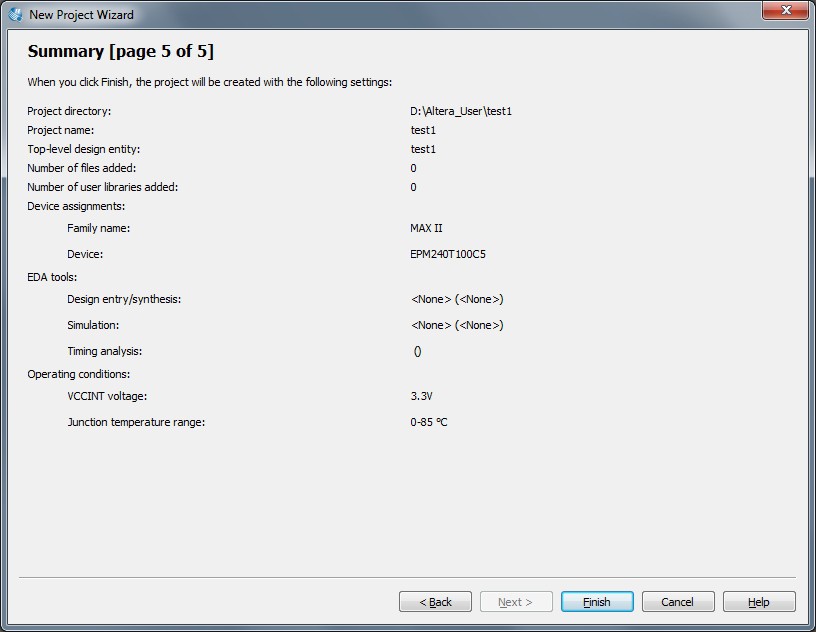
In the "Family" field select MAX II, in the "Package" field select "TQFP" and select in the field "Available devices" the row "EP240T100C5". Click "Next >" when done
![]()
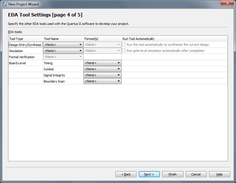
click "Next >" again
![]()
click "Finish" . Now you have an empty template and it's possible change the setting.
From the Quartus II menu select "Assignments" -> "Devices..."
![]()
click on the "Device and Pin Options..." button
![]()
set the "Enable device-wide reset (DEV_CLRn)" and "Enable device-wide output enable (DEV_OE)" check boxes. In this way you enable the "DEV_CLRn" key and the "DEV_OE" switch in the CPLD Fun Board.
These are two important functions: the first will reset all the FFs inside all the LEs (Logic Elements) with the "DEV_CLRn" key, and the second will enable the possibility to set all the CPLD pins to HiZ using the "DEV_OE" switch.
Some important notes about these two function:
- The DEV_CLRn key is active also when all the CPLD pins are in HiZ;
- When all the CPLD pins are in HiZ by means of the DEV_OE switch, the "DEV_OE" led is ON;
- If you doesn't enable the "Enable device-wide reset (DEV_CLRn)" check box, the DEV_CLRn key will not operate;
- If you doesn't enable the "Enable device-wide output enable (DEV_OE)" check box, the DEV_OE switch will not operate, but the DEV_OE led will turn ON anyway. This because it is not possible from the outside to know if this function is enabled or not.
Now you will set up the state of all the unused CPLD pins. "Unused" here means not referenced explicitly in the "programming" phase.
From the above windows, on the left side, choose "Unused Pins":
![]()
and in the "Reserve all unused pins" field set "As input tri-stated weak pull-up". This is the best (and safer) option for the CPLD Fun Board.
Now save this project. You'll use it later to set up a blink led example.
-
New PCB assembled and running
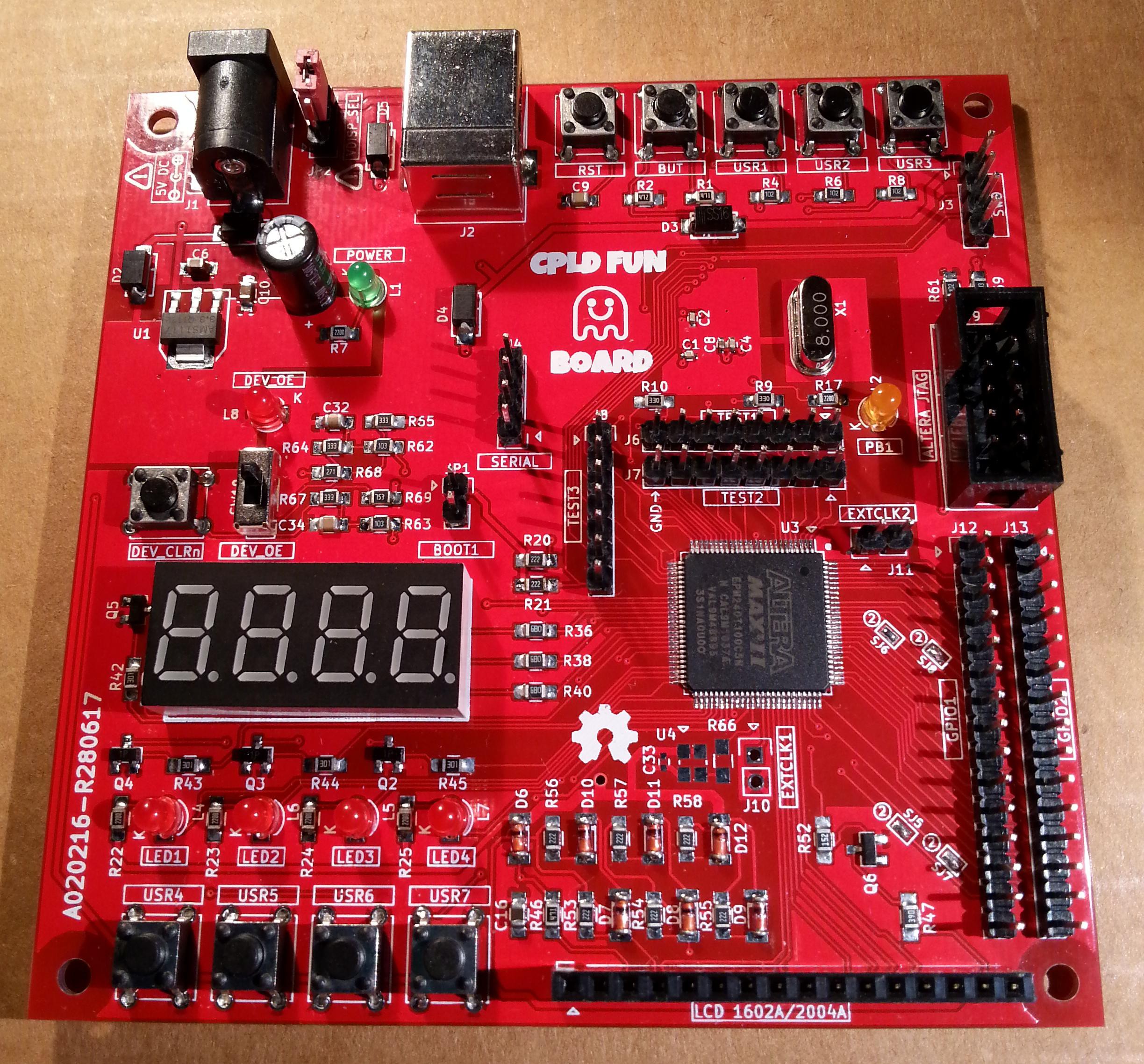
10/19/2017 at 12:21 • 0 commentsHere it is the new version:
![]()
![]()
And a short demo video:
Now it is possible use an EPM570T100 too, "configuring" the PCB with eight solder jumpers (see the legend on the bottom side of the PCB, or the schematic).
The capacitors C31 and C35 are required only for the EPM570T100, so if you use an EPM240T100 do not populate them (as in the board shown in the photos, using an EPM240T100).
Because currently I haven't any EPM570, when available I'll make an other board with it.
In the files section I've added the schematic and PCB Gerber files (traces width/clearance is 7mil/7mil).
There are also layout guides to help to assemble components for both the sides of the PCB, with both components reference and value (file PCB_Layout_Guide.zip).
The components list is here.
-
New PCB will support EMP240 and EMP570 CPLDs...
09/14/2017 at 09:09 • 0 commentsI've just finished the new PCB revision:
![]()
![]()
With eight solder jumpers (SJ1-8) it is possible now "configure" the board to use an EPM240T100 or EPM570T100 CPLD (the idea to allow the choice between an EPM240 and an EPM570 was suggested by Hacker404).
In the back side there is a short note on how use the solder jumpers.
I've also added a switch and a led for the DEV_OE signal, because using the previous board version I realized that it would have been more handy.
Now some more checks before send the files to the PCB service...
Arduino + CPLD = CPLD Fun Board!
Homemade low cost CPLD dev board (Arduino STM32F103 and Altera MAX II EPM240/EPM570 CPLD). Two dev boards into one.
 Just4Fun



 This is the environment:

 and complete the connections as in the following photo:


 Now rename the names of the input/output pins (pin_name1, ...3) as in the following photo, clicking twice on each name: