-
'light pipes' and calling this one done
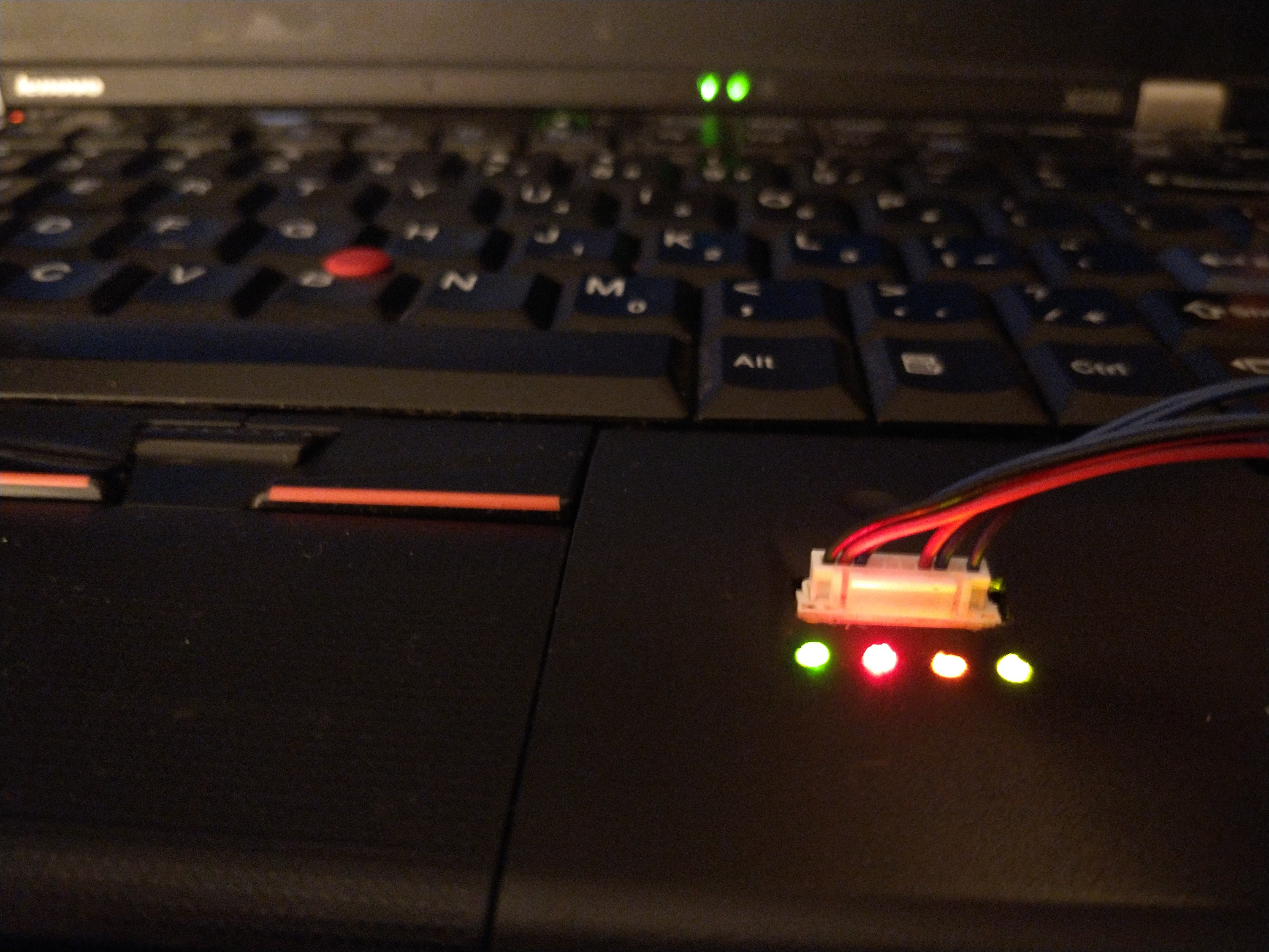
09/18/2017 at 02:25 • 0 commentsDrilled a few holes in my palm rest and press-fit a few ~4mm lengths of thick plastic fiber optic strand I had lying around:
![]()
[above: crappy light pipes installed, BMP messed with until all four LEDs light up. Left to right: power (green), error (red), activity (orange), usb-serial (yellow).
I may update this in the future if I end up trying it out with other Thinkpads, but for now this project is getting switched to 'complete'.
-
soldering xson8s sucks but the board works
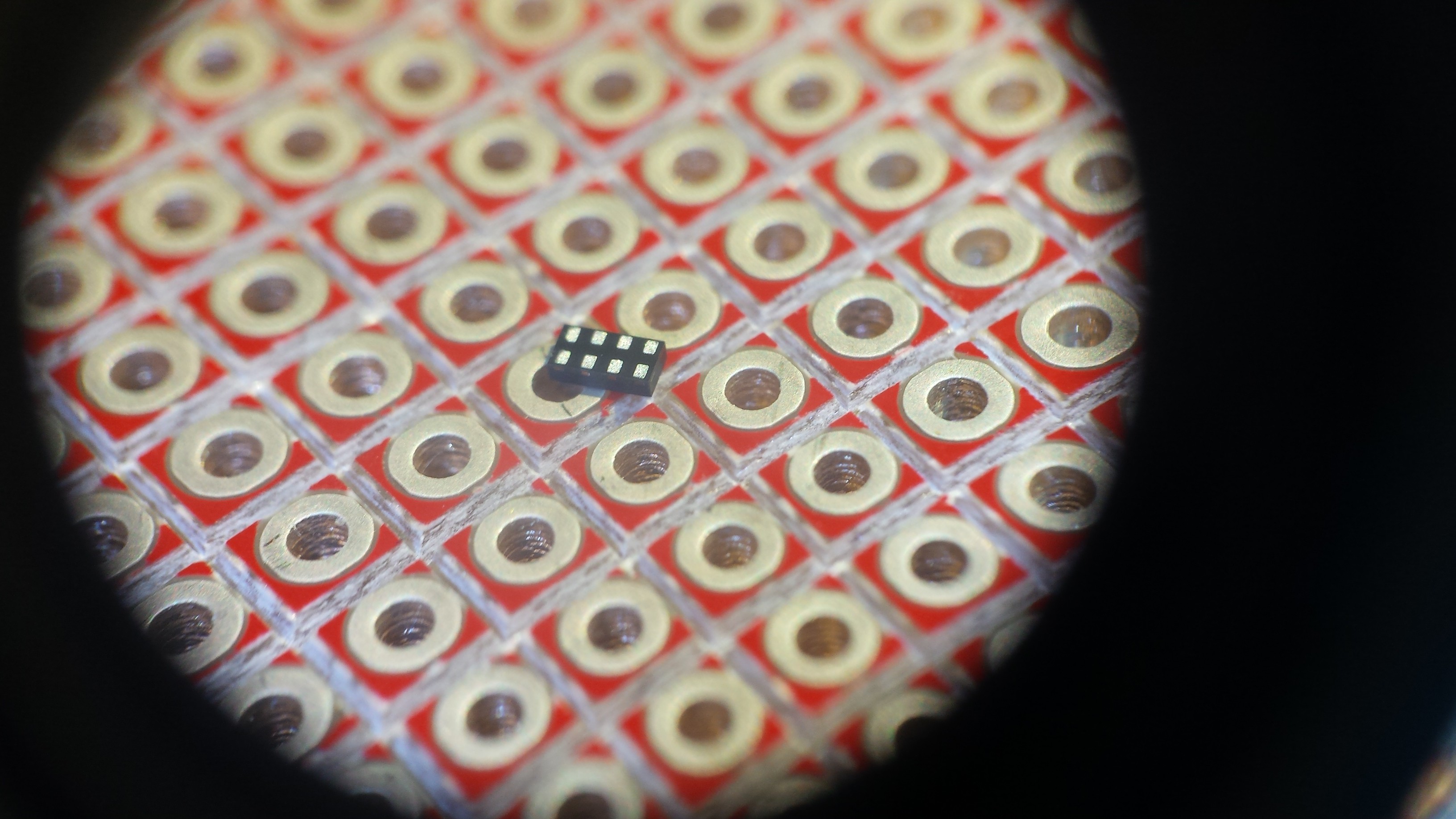
09/15/2017 at 21:31 • 0 commentsAs the title says, soldering the tiny XSON8-packaged level shifters was a real pain in the ass. I didn't make a stencil for TP-BMP but I did stretch the footprint out a bit, so I tried hand-soldering them but to no avail. You can probably see why:
![]()
[above: image of the bottom of the level shifter in XSON8 form, sitting on a standard 0.1" spaced board for scale.. Note that this is really an LGA, so unlike a QFN the pads don't actually extend to the side of the package. Not hand-soldering friendly.]
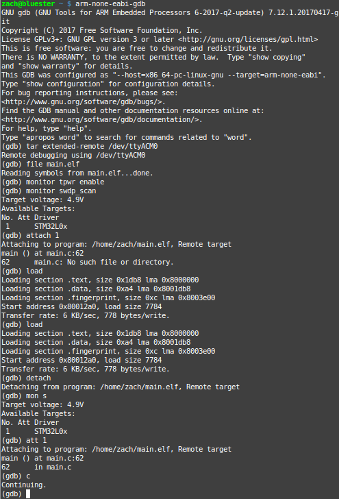
I probably should have gotten a stencil and started over with a fresh board, since I have a few extra. Instead, I bodged on a bit of solder paste and hit the components with a hot air gun. This didn't work at first, so I touched 'em up with an iron, tested the board, desoldered two of them, cleaned up the joints, etc .. repeat for a lot longer than I should have spent on this project. But finally...
[above: screenshot of using ARM gdb to detect, attach, program, and detach a #NeuroBytes Interneuron board. Yay!]
-
pcb layout
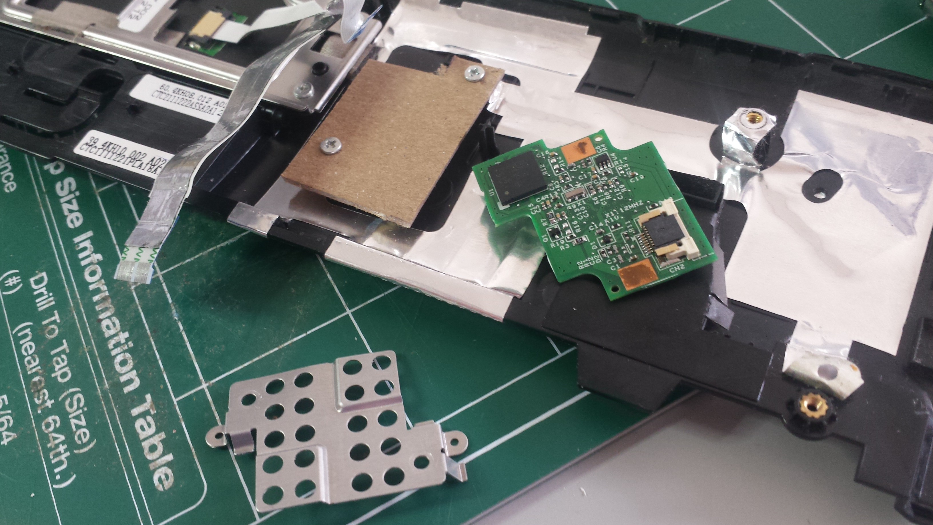
09/13/2017 at 21:38 • 0 commentsThis project is a layout-only exercise, so it starts with the Black Magic Probe Mini v2.1 schematics published in the FAQ section of the project's wiki. After reproducing the schematic in KiCad, the X220's palm rest was measured and test-fitted with a cardboard mockup:
![]()
(above: getting rid of the thumbprint reader/metal shield and replacing them with a cardboard template. Yes it kind of looks like a backwards Utah.)
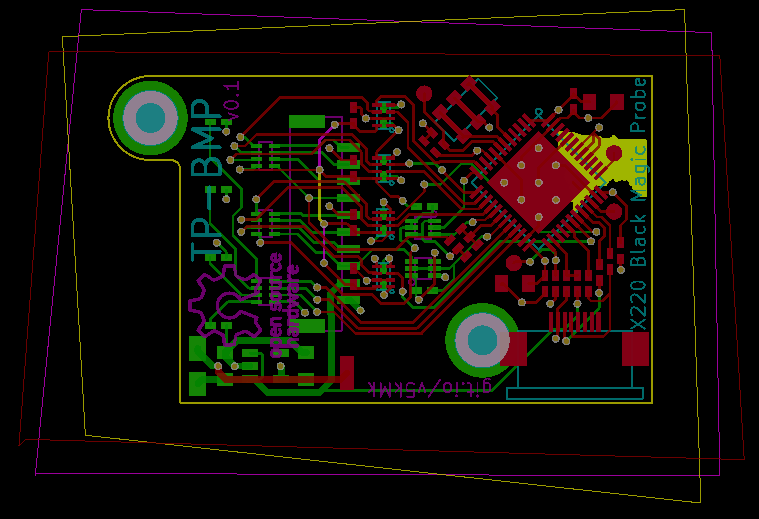
Putting everything in KiCad suggested that the shape and size above would work given the connector location constraint and the component footprints. This design is quite a bit larger than the original Mini and has components on both sides; this made PCB layout quite a bit easier than the Black Sphere design:
[above: a KiCad screenshot of the 4-layer board (sig-gnd-vcc-sig) with one middle layer track, which probably isn't ideal.]
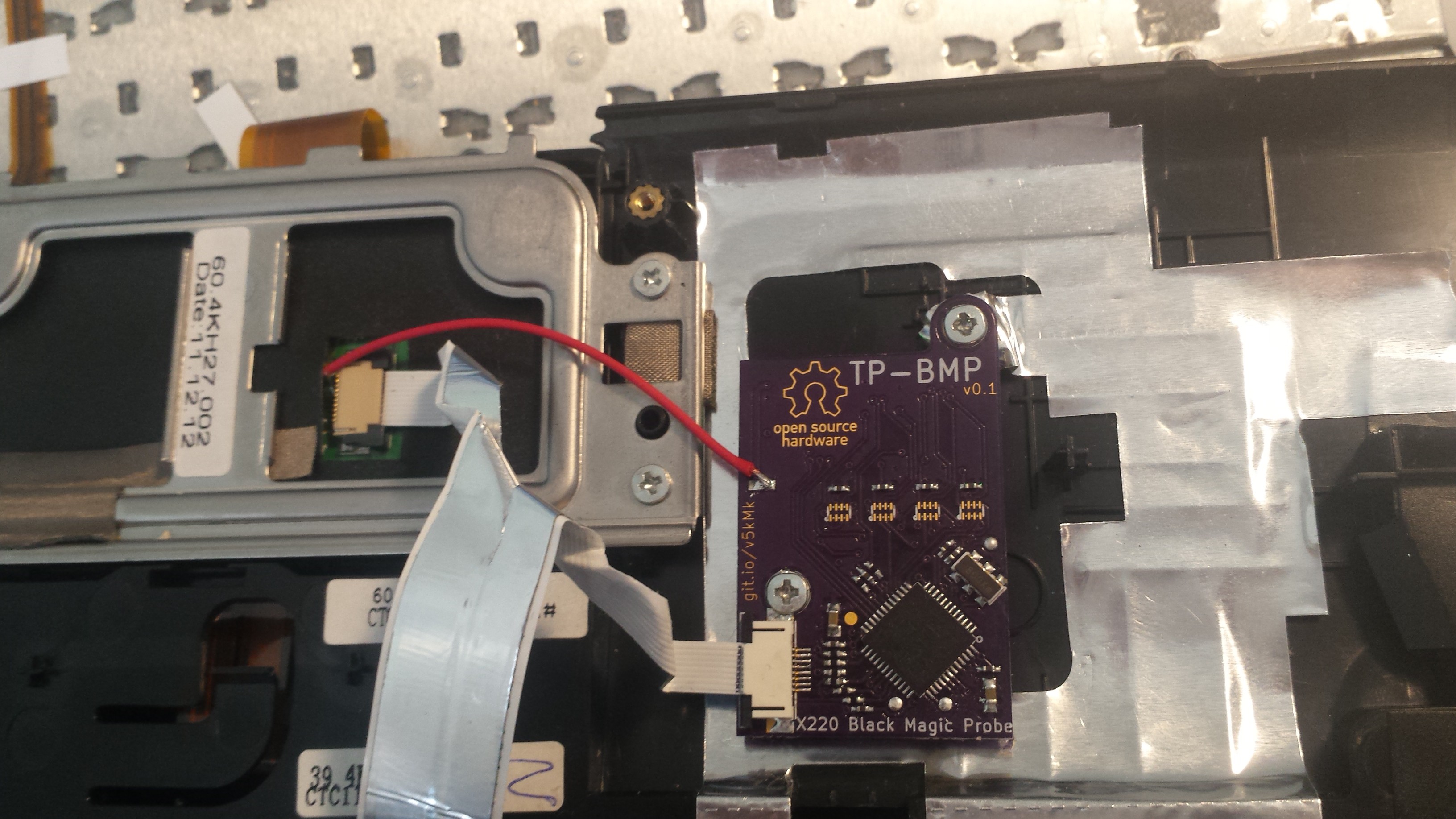
After reflowing the QFN STM32 and soldering the rest of the board together (other than the level shifters which are backordered, ugh), a fit check suggested that the hole spacing needs a tiny bit of adjustment but works well enough for v0.1:![]() [above: TP-BMP installed in the X220's palm rest. Note missing level shifters. Also the cutout for the fingerprint sensor had to be widened a bit to clear the 10-pin JST header.]
[above: TP-BMP installed in the X220's palm rest. Note missing level shifters. Also the cutout for the fingerprint sensor had to be widened a bit to clear the 10-pin JST header.]I forgot to take pictures of the firmware loading process; in the image above, one can see the test pads below the STM32 that were used for this process. A Discovery Board was used (well, its ST-LINK, at least) along with st-link to load the stock BMP firmware and bootloader binaries. After re-installation, the board enumerated (!!!), so now it's time to drill LED holes, finish the wiring harness, and solder on the level shifters (when they arrive).
-
time to find us some usb goodness
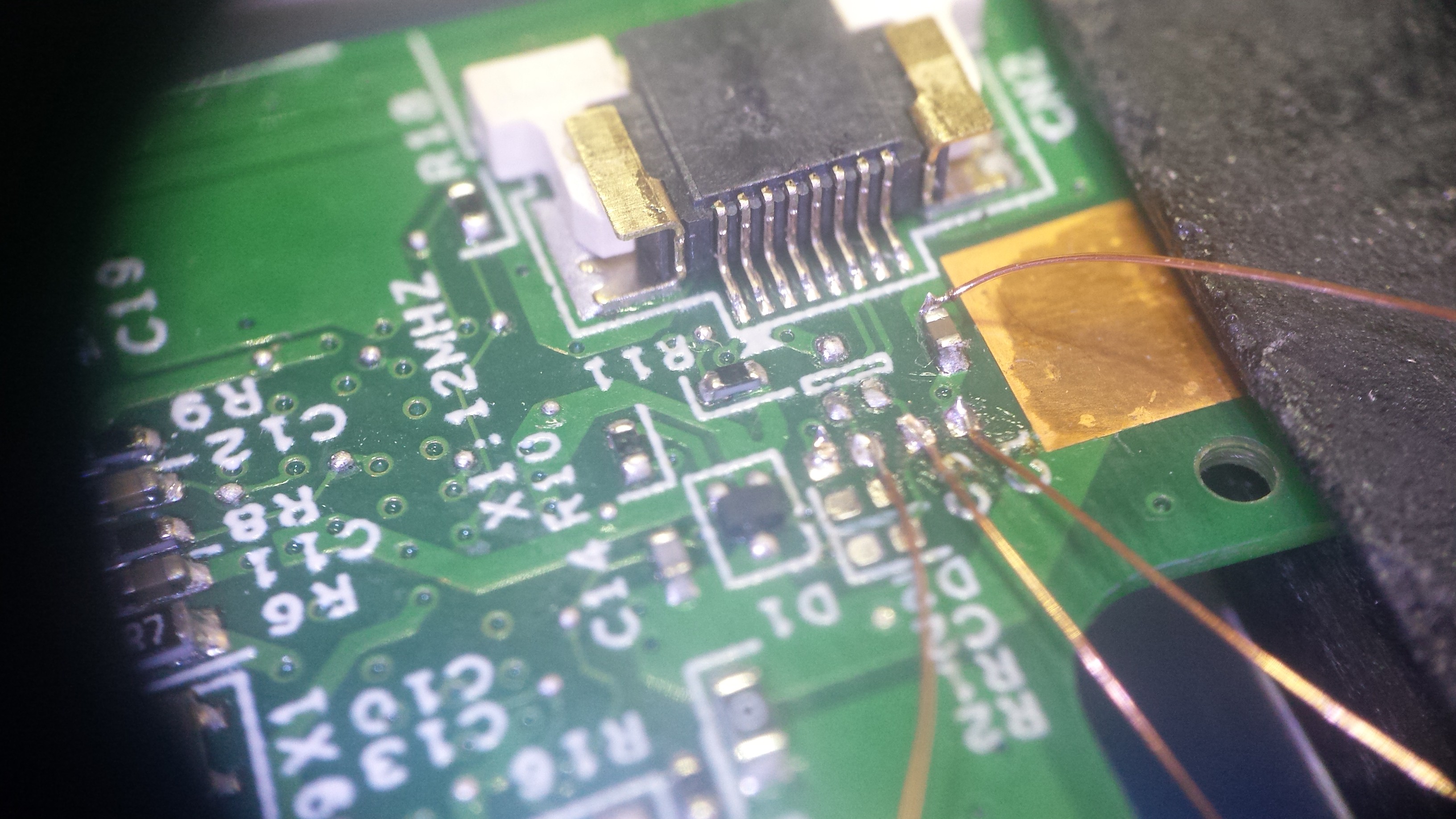
09/13/2017 at 20:25 • 0 commentsWhen I started this project, I had an inkling that the fingerprint reader spoke USB. To verify this, I popped the board out of my computer and tacked on a few test wires:
![]() [above: 10x loupe photo of the fingerprint reader PCB showing a few test wires]
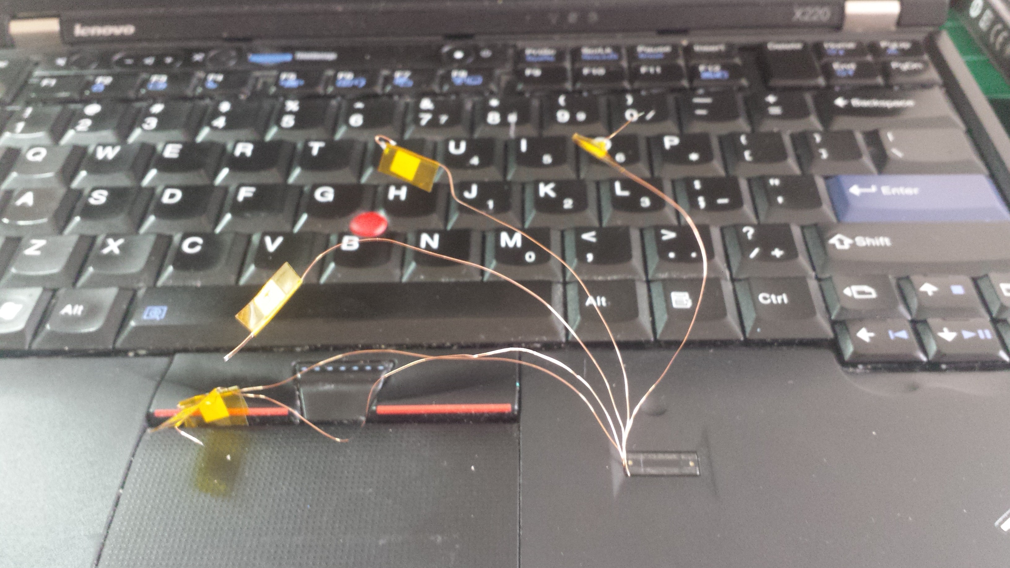
[above: 10x loupe photo of the fingerprint reader PCB showing a few test wires]I labelled the wires according to position on the FFC header, snaked them through the fingerprint reader cutout, and reassembled the computer so I could 'scope 'em:
![]() [above: testing potential USB traces, prior to getting over my fear of disassembling my laptop without disconnecting power/battery]
[above: testing potential USB traces, prior to getting over my fear of disassembling my laptop without disconnecting power/battery]This didn't tell me much, beyond suggesting that the fingerprint reader didn't require +5VDC. Most of the wires seemed to be +3.3VDC or ground, but a few appeared to have some interesting signals on them. I decided to butcher the fingerprint board and make an FFC header breakout so I could convince myself everything worked:
![]() [above: another 10x loupe shot confirming that breakout boards are for suckers]
[above: another 10x loupe shot confirming that breakout boards are for suckers]![]() [above: always looking for an excuse to carve FR4...]
[above: always looking for an excuse to carve FR4...]
Eventually, I bodged together a breakout and located the two USB data pins. I tested everything using a hacked-apart ST-LINK from an STM32F0 Discovery Board to program a #NeuroBytes Interneuron:![]() [above: an Interneuron connected via st-util (hence the green light on the Discovery board half). The +3.3VDC supply voltage didn't cause any issues for the ST-LINK, but it did mean that the Interneuron's LED was quite dim.]
[above: an Interneuron connected via st-util (hence the green light on the Discovery board half). The +3.3VDC supply voltage didn't cause any issues for the ST-LINK, but it did mean that the Interneuron's LED was quite dim.]
So... if you want a free 3.3VDC USB port instead of your Thinkpad's fingerprint reader, here's the pinout:[above: FFC USB pinout, if the cable has conductors exposed on the top and enters from the left.]
TP-BMP
Black Magic Probe remixed to replace the silly fingerprint reader on my X220. Might work on other Thinkpads too. ARM debugging for all!
 zakqwy
 [above: screenshot of using ARM gdb to detect, attach, program, and detach a
 [above: a KiCad screenshot of the 4-layer board (sig-gnd-vcc-sig) with one middle layer track, which probably isn't ideal.]
 [above: TP-BMP installed in the X220's palm rest. Note missing level shifters. Also the cutout for the fingerprint sensor had to be widened a bit to clear the 10-pin JST header.]
 [above: 10x loupe photo of the fingerprint reader PCB showing a few test wires]
 [above: testing potential USB traces, prior to getting over my fear of disassembling my laptop without disconnecting power/battery]
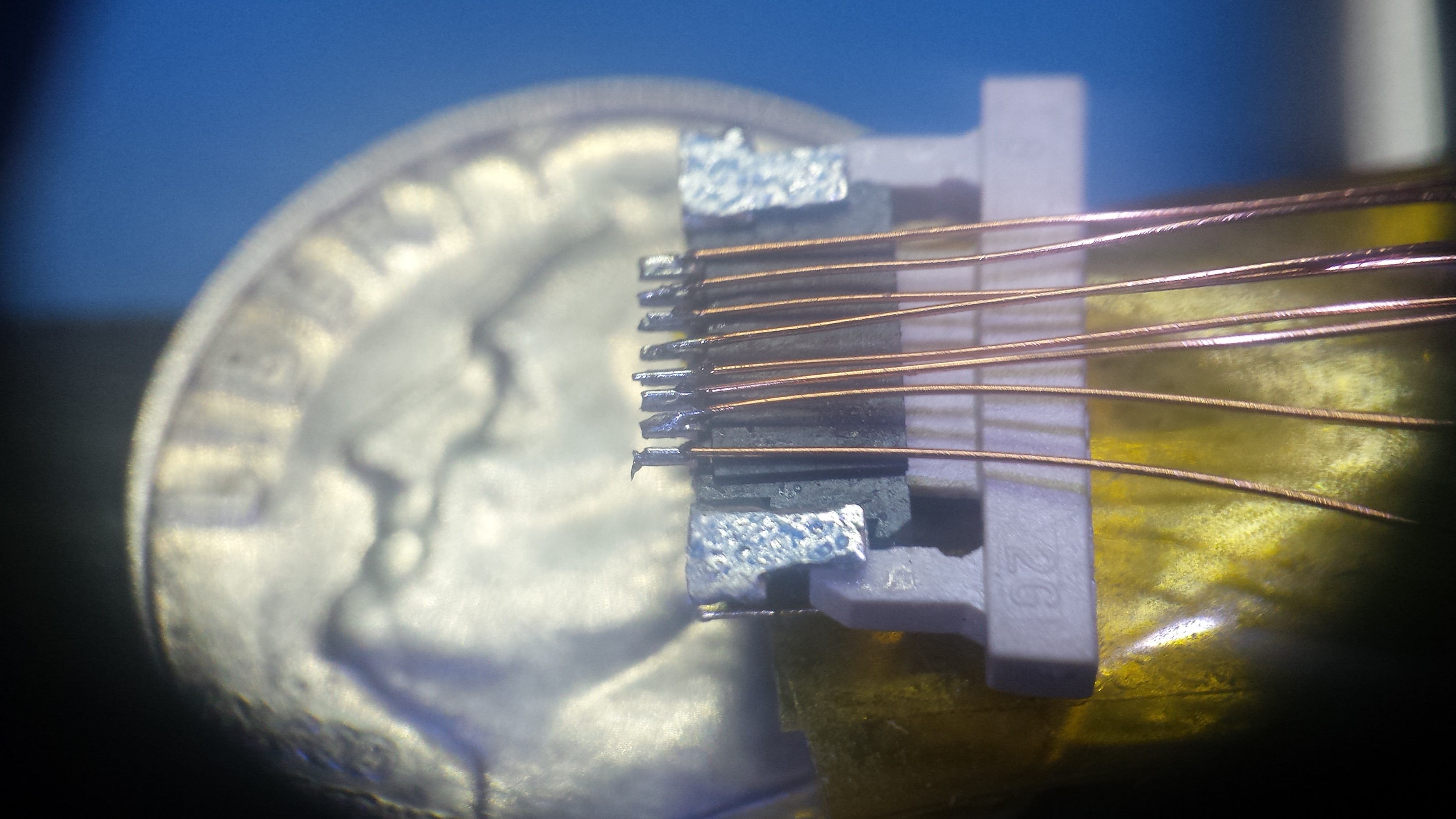 [above: another 10x loupe shot confirming that breakout boards are for suckers]
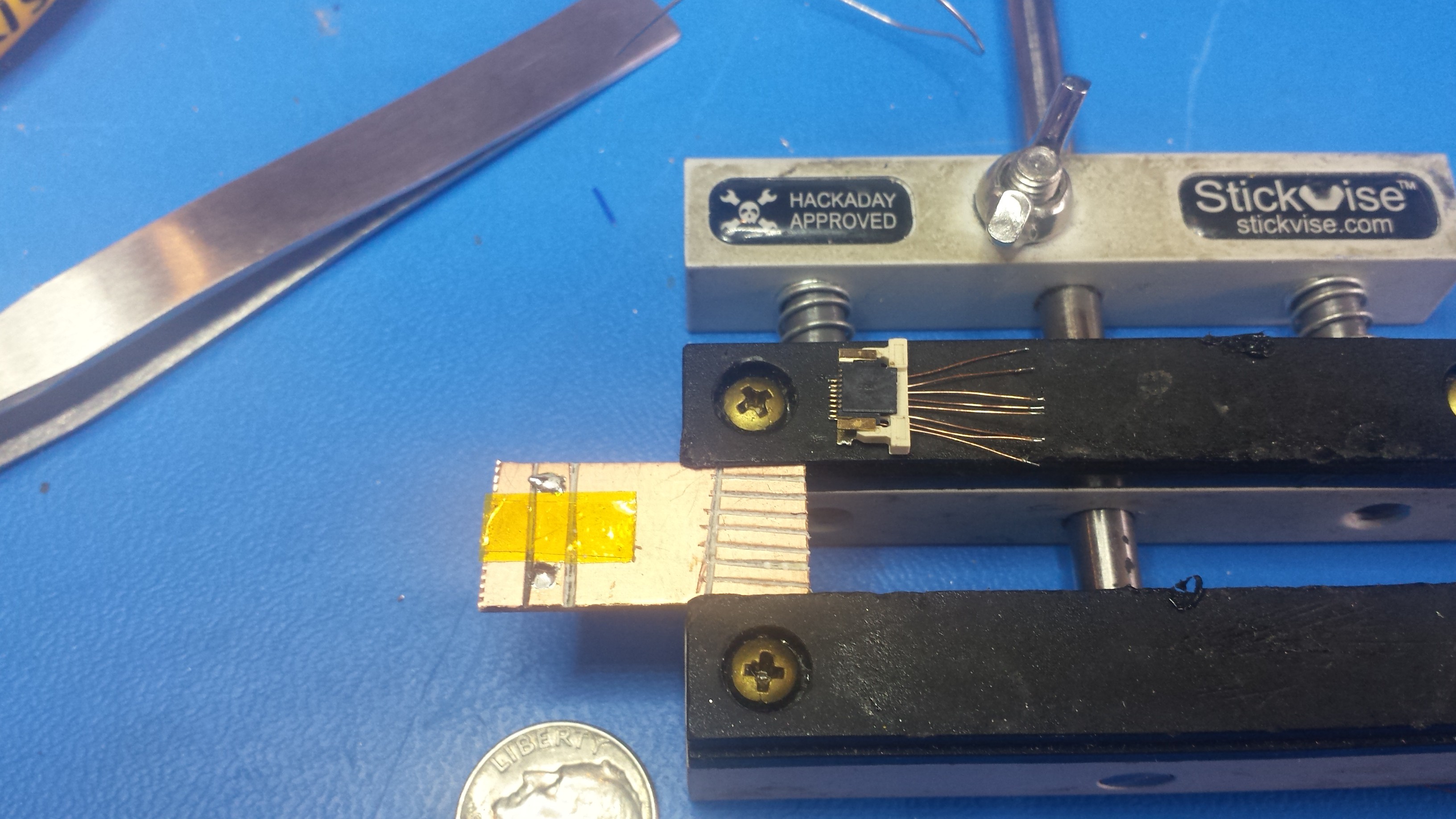 [above: always looking for an excuse to carve FR4...]
 [above: an Interneuron connected via st-util (hence the green light on the Discovery board half). The +3.3VDC supply voltage didn't cause any issues for the ST-LINK, but it did mean that the Interneuron's LED was quite dim.]
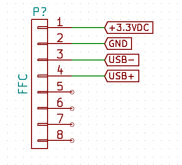 [above: FFC USB pinout, if the cable has conductors exposed on the top and enters from the left.]