Yann Guidon / YGDES
-
Need help with RES60 / РЭС60 relays
09/04/2019 at 23:35 • 17 commentsAt the start of 2019, I found a very interesting item on @qro_team 's eBay store : a single box of 40 low-voltage РЭС60 relays. I wish there were more !
It's the real deal : it's DPDT (unlike the РЭС15 which is only SPDT), it's very small (great for density) and the version I have can turn on at around 2.5V at half the current of the РЭС15.
The DPDT part is very important for several circuits, for example the incrementer for PC and the ALU. But today I focus on other less visible parts : the bit sense circuits for the memory arrays. The DRAM uses capacitors that will discharge in the coil and the lower current increases the reliability of the whole system (less sensitive to current leaks in the capacitors). The instruction PROM (on which I work at the moment) also benefits from a lower current because each line drives 16 bits and the aggregate current is then handled by a single relay... So if a current of 10mA is enough to trip one line sensor, the worst case scenario for the main driver is 160mA, which is within the tolerance of the РЭС15. It remains to be seen how long it remains reliable but this is another debate. I could make the "single point of failure" easy to replace.
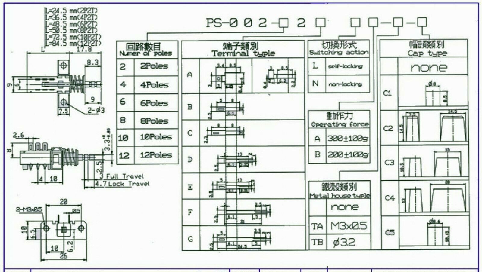
The РЭС60 I have are sold as "6 to 8V" with a coil that measures about 66 ohms. It's a -02 type (?) and all the others I find on eBay have a much higher voltage : 18V, 23V, 27V, 34V... They would certainly have a lower driving current but the voltage swing is not practical. I could try my luck if there are "12V" versions but I need another box because the 40 pieces I have at the moment is barely enough for the various circuits that require it... Who could help me ? @Artem Kashkanov ? @[skaarj] ? ...
According to this datasheet (and many others found online),
![]()
there must be a marking error on my box because the -02 is rated at 270 ohms and I measured coils in the 65 ohms range... but apparently I need a 12V version, with -02 or -08 type (I still can't get the difference).
I might have found -04 (lower voltage) that would be useful in the ALU so my -03 would be used as sensors, probably using pre-biasing, unless there is some magic reed relay that could save the circuit ? (Artem ? ;-) )
Correction : the box is marked "00.02" so according to the references I have found, it should be a 23-34V version. Measurements disagree... I don't know what happened or if the parts were repackaged but anyway, I have them :-D
20200129 : I received 25× РЭС60 relays but their coil is 800 ohms so 13V min.And I finally watch Curious Marc's video to see a lonely РЭС60 at 6:00 :-D
enjoy !
-
A Diode (P)ROM was (almost) built in a day
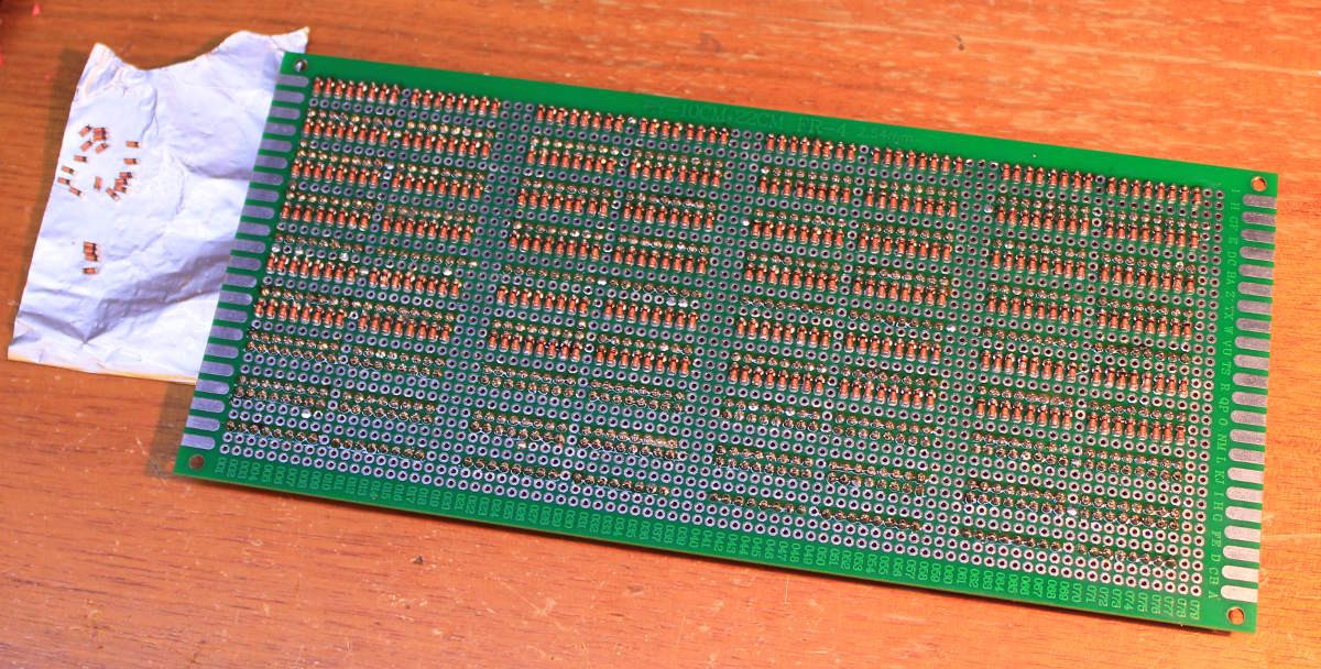
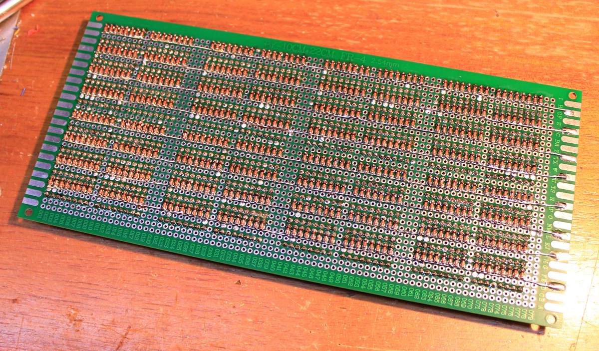
09/03/2019 at 12:35 • 0 commentsSo I tried to build a prototype and it was almost finished in a day :-)
32 instructions, 64 DIP-switches with 16 pins each, that's already 1024 soldering joints.
![]()
Then 512 diodes (LL4148), linked in 8 rows, make another kilojoints :
![]()
but it's not as hard as it sounds.
What is still missing is the 64 column wires and the connectors. I'll also add one LED per line.
Of course a dedicated PCB would ease assembly but this
- would be very costly
- I have more important other expenses
- I already have these parts in stock
- I don't want to waste money with a flawed PCB design that a prototype could solve.
Anyway with 32 instructions I'll have enough room to test interesting things and it's not as hard as it looks.
I want to make the board design modular, each board can be relocated physically on a backplane to change the address. There are 2 decoders, large MUXes for the lines and columns, that will not need changes, while the data boards can be of any type (DIP switches, solder joints or anything else I come up with).
-
Diode (P)ROM wasn't built in a day
08/27/2019 at 21:52 • 0 commentsAs I build the instruction assembler and disassember, I must also provide a way to store instructions. This was already covered in #YGREC16 - YG's 16bits Relay Electric Computer in the log PROM boards.
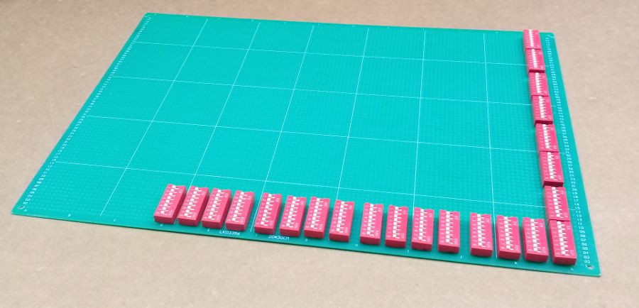
Things have evolved since 2017 and I now have a whole bunch of DIP switches (Log: I hope that's enough this time) and pretty large proto boards... I have just what is required to build boards with 16×4=64 instructions :-)
But let's look at how these boards must be organised. The YGREC8 has 16-bits instructions so a higher density than the 24 bits of the YGREC16. And there are only 256 addressable instructions. That's 256×2=512 DIP switches, I have more than 700 in stock these days :-)
Then the topology must be optimised to reduce the number of relays : how many lines and columns ?
- 1 column and 256 lines : 1 huge MUX256, or 255 relays. HUGE...
- 2 columns and 128 lines : 1 huge MUX128 and 16 relays to select the column, or 143 relays. Better but still not optimal.
- 4 comumns and 64 lines : 1 large MUX64 and 16×MUX4, or 63+(16×3) = 111 relays. Good.
- 8 columns and 32 lines : 1 MUX32 and 16×MUX8 = 31 + 16×7 = 143 : the column MUX gets too large now.
So be it : the PROM cards are organised with 4 columns.
![]()
I'll try to build a 8×4 board to get started... because I also need to build the 2 big MUXes for lines and colums. Where are my boxes of SMD diodes ? :-D
-
More assembler panel stuff
08/25/2019 at 13:09 • 12 commentsI have received and tested all the interlocked switches :-)
and I'm updating the layout and dimensions, using the diagrams I have found on the web:
![]()
So far the layout of the panel is:
![]()
but many questions are still in the air...
I can print with my laser printer to the exact scale so this will be very useful: no need of a CNC ! but it only moves the problem around.
How can I transfer the toner to the front panel (aluminium) for the labels of the buttons ?
I added the "SEL" button : it's a SPDT switch that selects which circuit gets the power/signal, either the assembler panel or the program ROM. That makes now 3 switches (IMM8, NEG and SEL) and I haven't decided/found which model to use. I need a low-force, high-endurance switch with a long lever (10mm or 12mm ?) so the drill diameter is undetermined (until I find THE model that fits).
The SEL button changes several things, because initially I wanted to use a 16-pole dual throw switch to select the value sent to the instruction decoder. The operating force and endurance would not be satisfying because I want to alternate between both sources easily and fast. Now the instruction bus is shared between the ASM panel, the instruction ROM and the eventual electronic/remote interface.
For the YGREC16 with 24 instruction bits, I started with positive logic, then realised it would be more complex for the driving electronics so I changed to a different driving system where PNP transistors just pull the signal to 0V. But overall this is not easy to manage and a return to "positive logic" seems unavoidable.
Another consequence is that the outputs of the asm panel must be "diode protected" because some signals can be shorted by the switches. This is not a problem when the panel is operated alone but it will interfere in some cases with the ROM and the external interface. Another version of the diagram is necessary... So here it is!
![]()
There are now 38 diodes now. It is not a tragic increase but there is a good side effect : all the signal paths have one diode drop, everything is now balanced !
-
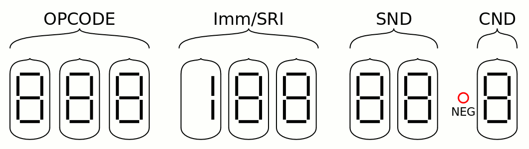
The disassembler panel
08/08/2019 at 02:31 • 0 commentsAs you can see at Log: Don't go full Numitron ! Unless... OK whatever., I started to design the disassembler and I totally renewed the look:
![]()
This version now shares a pair of Numitrons to display either the SRI or the Immediate field, which saves a bit of room and 2 tubes but adds some complexity in the decoding logic (yet not enough to scare me, of course). The above display is not compliant with the normal assembler but close enough and it gets the job done :-)
I draw a lot experience from the #Numitron Hexadecimal display module so I know what to expect and what to do to display the desired patterns on the 7 segments. There is no technical challenge anymore to display the CND, SND, SRI and Opcode fields, but it's still a lot of work, in particular for the Opcodes: this decoder not only must display 19 words on 3 tubes, but also sends control signals to enable the other fields.
It's going to be small and gorgeous but behind the front panel, the electronics will be pretty dense and draw a significant amount of power...
Damnit I forgot that IN/OUT have 9 bits of immediate address...
![]()
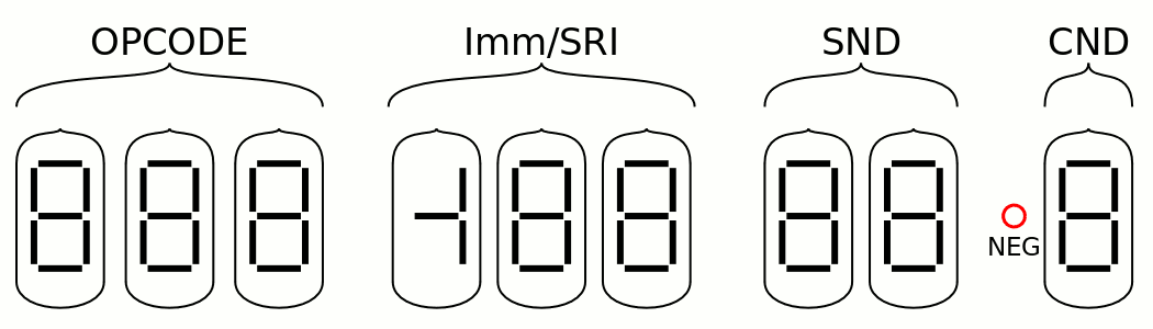
The Imm field will create more problems, on top of the multiplexing with the SRI decoder. The field must select the width between 4, 8 and 9 bits. The last case is not a problem because an address is just a positive number. Imm4 is sign-extended to 8 bits (easy: 4 relays) but should Imm8 be represented as a signed number ?
Then there is the special case of Add imm4(>=0) where Imm4 is incremented.
The easy way is to simply display the number as is, and forget about it, though the display would not be accurate. It would even be misleading.
But then, if the Add correction or the negative display are implemented, an increment unit is required. And negative numbers require a XOR to transpose to positive numbers. This means more circuits in front of the display modules...
But with negative numbers, the added Numitron can have another segment used, for the sign bit:
![]()
To keep the system modular (and help with development, debug and repairs), I think I'll make 3 modules with 3 Numitrons each, with identical connectors. I can then develop all 3 groups in parallel.
The connector is probably IDC 2×13 : each Numitron has 7 segments + 1 common signal, or 8 wires, and 3 Numitrons need 3×8=24 wires. Add two positions for a pair of pins for the optional red Glühbirnchen and we have exactly 26 pins.
-
Updated wiring of the new assembler panel
08/04/2019 at 16:41 • 0 commentsI nailed it !
![]()
I solved a "bug" and I now use "normal" hexadecimal encoding knobs. This required a big redesign... There are now 29 diodes but only one per signal so I can use old, low-current point-contact D9K.
Another big difference is a rotary 4-poles 3-throw selector ! It selects between the Imm8, Imm4 and Register forms. I could use interlocked switches as well but their mechanical installation might be more complex, more holes and alignment...
I'm only missing one row of 8 switches for now, but I can start the construction :-)
-
ASM panel dimensions
07/31/2019 at 00:40 • 2 commentsAs I received the buttons, I was able to not only get electrical information but also dimensions. I updated the layout:
![]()
The 50 buttons easily fit in a 18×18cm square so 20×20cm is a safe dimension for this panel.
Remember that it's only the instruction, and more things are done in other panels :
- The disassembly panel shows the instruction being sent to the core (it's the reverse of the ASM panel)
- The control panel selects the source of the instruction, generates the clock, sends the clock pulses to the core (one-shot, several ones or continuously)
- The debug panel has several event counters that can stop the core...
- More panels display the inner state of the core
-
Interlocked switches galore !
07/29/2019 at 01:44 • 1 commentI received quite a few switches and more will come later !
![]()
These are 10 interlocked switches, with their caps, and they are just like I wanted :-)
2 of them will be used for the opcode selector.
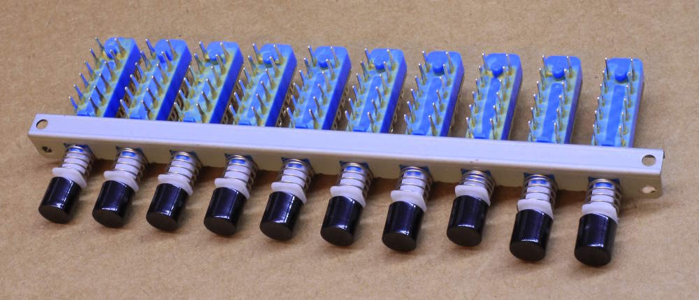
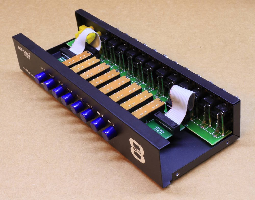
For the other selectors I needed somethign more simple and pre-made, and I have found it in the form of the 8-channels video selectors. And I have a good surprise ! Look:
![]()
I expected the box to contain a single PCB but there are two, making the switches assembly very easy to remove !
2 screws and 2 connectors to remove, and there you have the module :-)
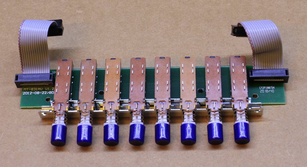
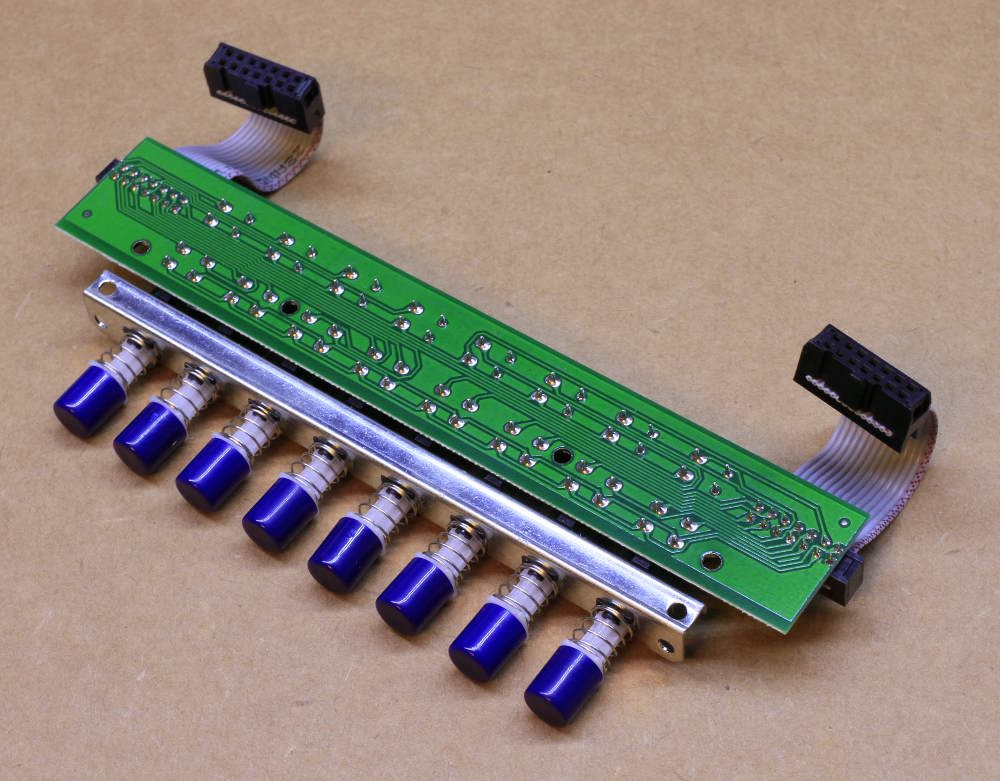
![]()
The traces are easy to follow and they are already conveniently wired for my purpose :
![]()
The SRI, SND and CND fields are 3 bits wide, and the selector outputs 3 bits, which is a great match.
I can wire the switches' inputs to a common rail, such that the 3 output bits will contain the binary code of the selected button. I can also bind the boards together to make a more sturdy structure (I have 2 but need a 3rd for the conditions).
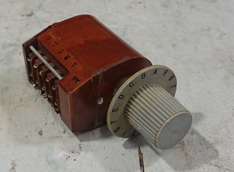
There is a last technical problem though, with the hexadecimal encoder : the lower nibble requires a type of switch I don't own... But @Artem Kashkanov has the perfect part ! From Russia, of course ;-)
![]()
This selector has individual SPDT switches for each bit, making my diodes hack possible :-)
I'm still missing a few extra switches but they'll come soon enough.
At least I successfully designed a fully-passive assembler panel, with only one diode drop on certain signals, and no requirement of external power (no relay or other logic). The panel can work with relay logic, transistors, TTL...
Time to think about the disassembler panel now ;-)
I have easily modified 2 8-ways selectors !I can say it works very nicely :-)
I'm waiting for the delivery of the 3rd module so I can have all the necessary buttons for the SND, SRI and CND fields.
-
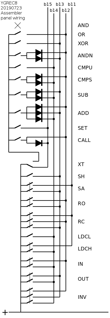
More wiring of the new assembler panel
07/23/2019 at 02:32 • 0 commentsI figured a few things...
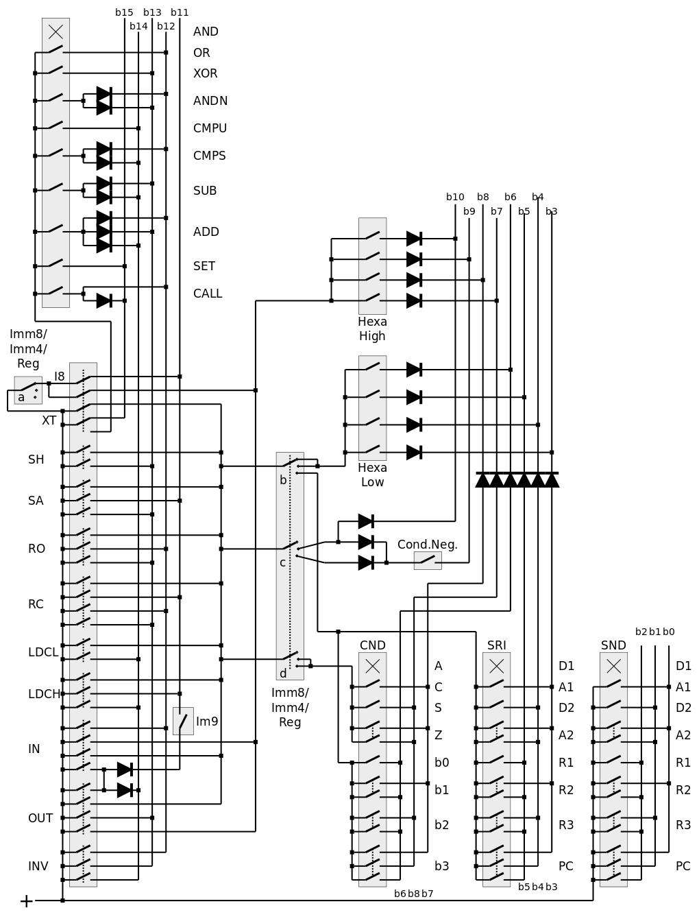
Here is the aggregated schematic for the opcode field :
![]()
It might look complex but most of the complexity has been examined in the previous log and it's basically a pair of binary encoders that have been chained through the XT button.
The tricky part is the simultaneous selection of buttons from both rows : some combinations would disrupt the binary code. This occurs when the "lower row" (AND through CALL) has one button pushed with a code that has more than one set bit (ADD, SUB, CMPS, ANDN). There is a potential path that is now broken by 10 diodes. And since the locked switches work together, only one switch is now required.
The "upper row" OTOH doesn't need diodes because the switches are interlocked. There is no place where different signals are brought together, except when a switch is pushed.
I'm working on the other switches...
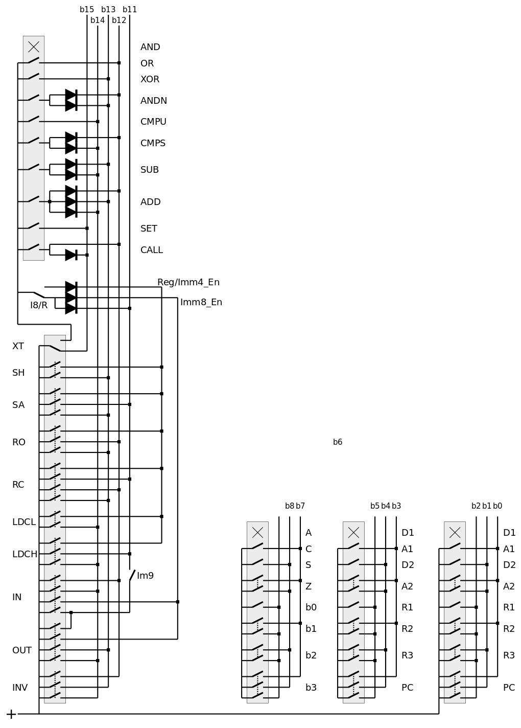
More schematicsing :-D
![]()
Going further, I added the dual hex encoders and tried to join everything together:
![]()
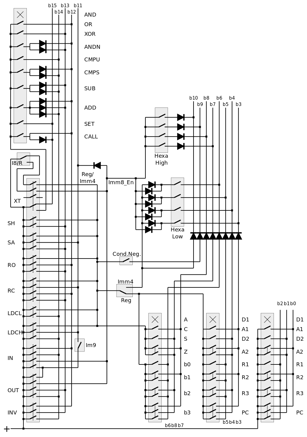
It's almost complete. b2,b1,b0 didn't change, nor did b15,b14,b13,b12,b11. The SRI field (and the LSB of the condition) can be combined with the lower half of the immediate field, while the condition field (plus a couple more bits) can be combined with the higher half.
However the simultaneous activation of the lower half for both Imm4 and Imm8 is more complicated and not yet implemented. The trivial version would use another diode, so the total drop would be 3 diodes !
I need a method to reduce this drop, I suspect there is a way to keep it down to 1 drop but I need to test it...
And I should switch from dia to EAGLE :-D
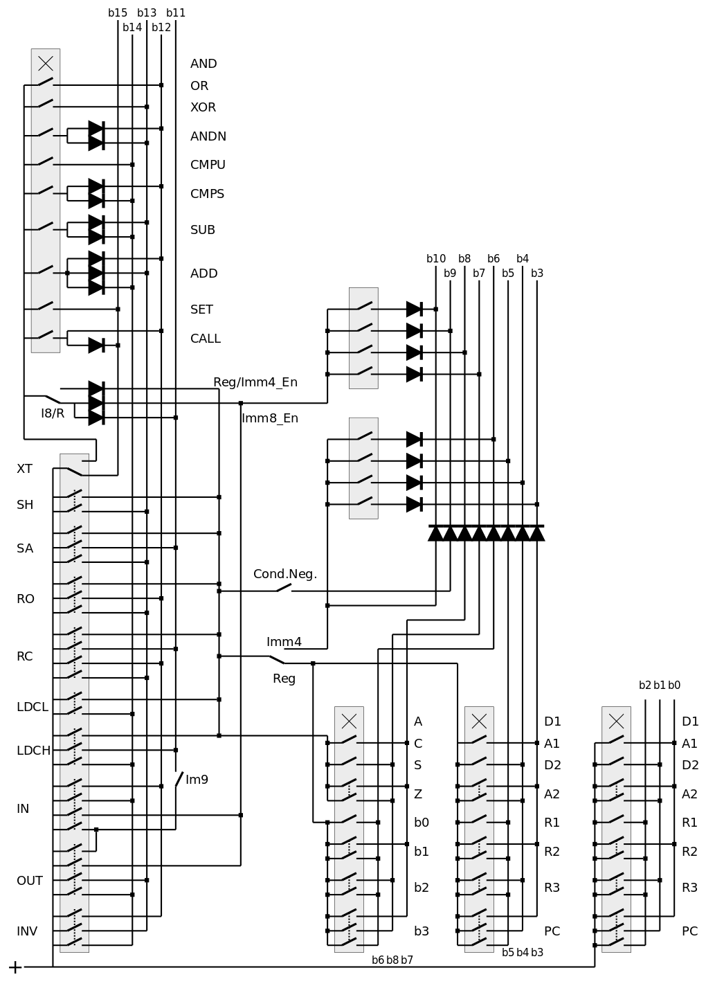
I solved a potential problem caused by several diode drops in series :![]()
The free switches for the XT button isolate the main signals and prevent the use of diodes. The hexadecimal encoder requires separate switches, so each signal can be driven by a pair of diodes (instead of one diode at the output).
There is one remaining switch and I wonder how to use it to remove more diodes...
-
Wiring the new assembler panel
07/20/2019 at 20:28 • 0 commentsAs mentioned in A new assembler panel, I'll soon (hopefully) get a bunch of 4PDT interlocked buttons !
I have already assigned their function but how will I make them work ? Electrically, I only want to have switches, eventually some diodes, and I would love to have the panel use the least power possible, which means ideally no relay. I hope that the panel can be reused for other technologies with the least amount of changes.
The critical information is contained in these 2 diagrams :
![]()
![]()
Already we can see 2 fields that are (almost) fixed :
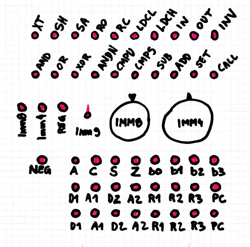
- The SND field uses 3 bits and a row of 8 buttons that can directly encode the binary code. The 4PDT switches are enough to encode the 3 bits easily. The question is settled and the same system will be used for the SRI sub-unit.
- The Opcode field has 19 codes (and as many buttons). Only RC and INV use 4 set bits so the 4PDT has some spare room, that we need indeed !
There is no interlocked switch with 19 buttons. The most I have found is 12 so I have chosen to use a pair of 10-buttons rows.
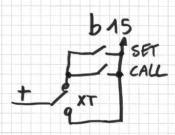
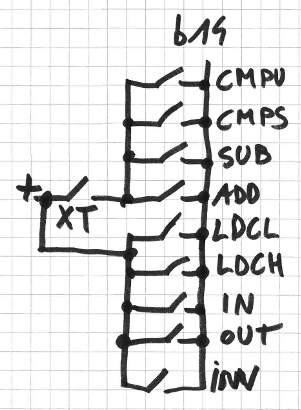
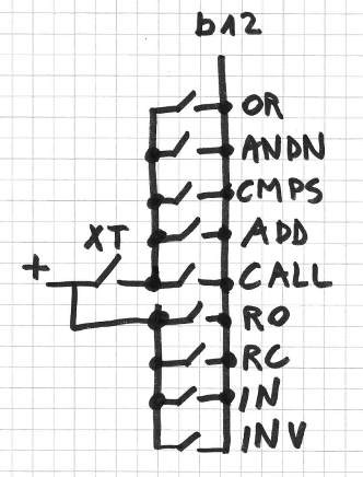
- The upper row contains the SH/SA/RO/RC/LDCL/LDCH/IN/OUT/INV opcodes. That is 9 opcodes. Each 4PDT switch can directly encode the binary value, except bit 15 which is always 1.
- The 10th button of the row is not an opcode but an "escape" button. Let's call it XT, it's an extention that selects the other row (which is the most used anyway) so it's not operated often. The 4PDT switch sets bit 15 to 1 when released (selecting the above opcodes), and otherwise activates the I8/R and Imm8 field.
- The lower row contains the AND/OR/XOR/ANDN/CMPU/CMPS/SUB/ADD/SET/CALL opcodes. Only 3 of the dual-throw switches are needed. The 4th bit remains unused.
How will this work, electrically ?
The panel uses "positive logic" where you implement a bit set to 1 with an electrical contact to an extra signal (usually a bus/rail, such as a positive voltage source). The switches will steer each instruction signal to the common voltage, depending on its encoding.
We can already write some truth equations for the most significant bits of the instruction word :
- b15 = ( XT & (SET | CALL))
| /XT - b14 = ( XT & (CMPU | CMPS | SUB | ADD))
| (/XT & (LDCL | LDCH | IN | OUT | INV) ) - b13 = ( XT & (XOR | ANDN | SUB | ADD))
| (/XT & (SH | SA | RO | RC | OUT | INV) ) - b12 = ( XT & (OR | ANDN | CMPS | ADD | CALL))
| (/XT & (RO | RC | IN | INV) ) - b11 = ( XT & I8/R)
| (/XT & (SA | RC | LDCH | ( IMM9 & (IN | OUT) ) ) )
As usual the OR operator "|" is implemented by parallel switches, while the AND operator "&" connects switches in series.
The terms contain XT which means the Normally Open side of the XT switch. So XT is a MUX for two sub-buses (b14,b13,b12).
Due to the interlock mechanism, /XT is redundant because it is always off when SH/SA/RO/RC/LDCL/LDCH/IN/OUT/INV opcodes are selected. However the 10 other opcodes are not interlocked and XT must disconnect the affected bits to prevent the other row from interfering.
Updated equations:
- b15 = ( XT & (SET | CALL))
| /XT - b14 = ( XT & (CMPU | CMPS | SUB | ADD))
| LDCL | LDCH | IN | OUT | INV - b13 = ( XT & (XOR | ANDN | SUB | ADD))
| SH | SA | RO | RC | OUT | INV - b12 = ( XT & (OR | ANDN | CMPS | ADD | CALL))
| RO | RC | IN | INV - b11 = ( XT & I8/R )
| SA | RC | LDCH | ( IMM9 & (IN | OUT) )
This is translated into the following diagrams :
![]()
![]()
![]()
![]()
![]()
The good news is : there is apparently no need for a complex switch for XT because its signal can be shared with several subsignals, thus saving switches...
The bad news is : to prevent certain cases of feedback/bypass (despite the use of independent switches) the output of XT must be guarded with diodes.
However, there are multiple switches per button so the number of diodes is kept low. Here is the census of the usage of SPDT switches per opcode (so far) :
AND: 0
OR: 1
XOR: 1
ANDN: 2
CMPU: 1
CMPS: 2
SUB: 2
ADD: 3
SET: 1
CALL: 2
SH: 1
SA: 2
RO: 2
RC: 3
LDCL: 1
LDCH: 2
IN: 2
OUT: 2
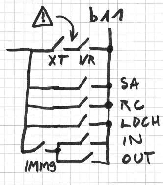
INV: 3OTOH the XT signal must be split into 5 diode-protected paths.
IN and OUT each use only 2 SPDT switches and 2 are left so each can feed (through a diode) the rotary encoders for IMM8.
XT also can enable the IMM8 encoders through the I8/R switch and 2 diodes. There are 2 encoders :
IMM8_hi = IN | OUT | ( XT & I8/R )
IMM8_lo = IN | OUT | ( XT & I8/R ) | I4/R
Due to the nature of the Hex switches, each output bit must be guarded by a diode as well...
Another interlocked switch selects the format : I4/R, I8/R and REG (they are mutually exclusive).
I8/R is only available in XT mode and otherwise defaults to I4/R mode.
The SRI field (as well as b6) is enabled with
SRI_en = REG & /INV & /IN & /OUT
This uses inverted logic and probably one of the spare/free SPDT of INV/IN/OUT.
Note : I have ordered 8PDT switches for the format selector because I thought it would be useful for actually MUXing the signals but it is not interlocked with XT and others and IN/OUT/INV would not reset the format to IMM8... Diodes seem to be necessary to enable the REG, COND and IMM fields.
The SND field is decoded with the following circuit :
![]()
The SRI and CND fieds are identical with some differences :
- The + is not tied directly to the power supply but to a diode-guarded contact of the REG switch
- The CND field is split, depending on the REG switch. The Bit0, Bit1, Bit2 and Bit3 options are enabled by REG (the b3 signal is switched) because otherwise the bit is used for the bit3 of the immediate (in IMM4 and IMM8 mode).
.
.
.
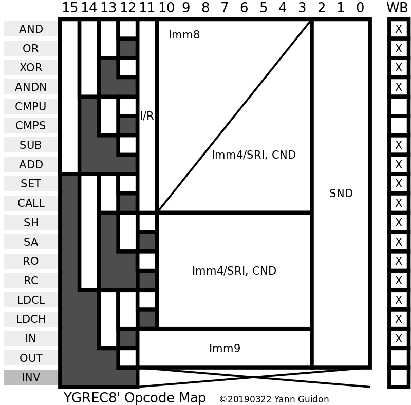
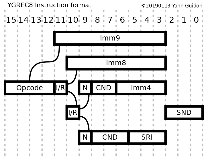
YGREC8
A byte-wide stripped-down version of the YGREC16 architecture