Since the lookup/jump table uses only one index, we can use A1 again to point at other things and preload the X and Y before the jump:
Select_direction:
  set X_Head A1
  set D1 R2
  set Y_Head A1
  set D1 R3

  set last_choice A2
  in buttons R1 ; read the external state
  and 15 R1 ; mask only the relevant buttons
  set D2 PC IFZ ; jump to last choice if no button
  add (jump_table-1) R1
  LDCL R1 PC ; lookup and jump
And now that the "default" choice is handled individually, the jump table could be relocated and save one instruction in the loop. The very first, unused, entry can be a jump to the initialisation code.
.ORG 0
  set init PC ; jump over the jumptable
; 0000 is already decoded
.DW Top_Handler     ; 0001 (it's a priority encoder)
.DW Right_Handler   ; 0010
.DW Top_Handler     ; 0011
;.......
.DW Top_Handler     ; 1101
.DW Right_Handler   ; 1110
.DW Top_Handler     ; 1111

init:
  set X_Head A1
  set (MAX_X/2) D1
  set Y_Head A1
  set (MAX_Y/2) D1
;...
The handlers can now be elaborated a bit:
Top_Handler:
  SET ($+1) D1
  ADD -1 R3
  SET -1 PC IFC ; jump to failure if negative
  ; ...

Right_Handler:
  set ($+1) D1
  ADD  1 R2
  CMPU (MAX_X-1) R2
  SET -1 PC IFC ; jump to failure if overflow
; ...

Bottom_Handler:
  set ($+1) D1
  ADD  1 R3
  CMPU (MAX_Y-1) R2
  SET -1 PC IFC ; jump to failure if overflow
; ...

Left_Handler:
  set ($+1) D1
  ADD  -1 R2
  SET -1 PC IFC ; jump to failure if negative
; ...
The address -1 in the code is a trampoline to the routine that handles the end of the game:
Failure:
  ; play the defeat song here.
  HLT

.ORG 255
  set Failure PC
This way, the immediate address is short and the jump can be conditional, called from about anywhere at no cost. The addresses 0 to 7 are already allocated to the priority/jump table, but there are 7 more "short addresses" for trampolines to other routines.
Now comes the big problem. The memory.
There are only 256 bytes per bank and only 2 banks by default. To get things going, we assume the playground is only 16×16 sites so one site is one byte. This is enough to store the required information since this buffer does not directly represent the graphics (each dot is black or white, controlled externally).
Each site needs to store the following information:
if the site is a "body" part (1 bit), and if so, the direction to the next one (2 bits)
if the site is a candy (another bit) (we can't represent a poison/trap with only 2 colors)
That's 4 bits only out of 8 and we will see later how to compact them. Let's first lay out the logic and solve addressing later.
For this 150th log, the new assembler lets us put everything together and consider a larger program than the short examples we've seen so far. So it's time to implement this Snake game, at last!
But it's also a sort of "code golf" for two reasons:
there is not much space for code and data
the code is expected to run on a very slow machine (the relay-based one, not onlu the FPGA)
The relay machine is expected to reach maybe 20 to 30 IPS (instructions per second, yes) which leaves no headroom at all for a game loop, 20 instructions per loop for a 1Hz refresh rate. So that's maybe 30, maximum 64 instructions to store (or program on DIP switches). Yet the YGREC8 is not designed for the Ultimate Code Compactness of All.
The first thing to determine is the direction. Already it becomes clear that the constraint of keeping the shortest possible execution time requires 4 separate code paths, otherwise there are many redundant or useless tests. So some duplication will appear but I don't think the size overhead will be significant, because there is more to do than steer the worm.
Another part is about "drawing the snake". This is common with the 4 code paths. This can be reduced to two steps :
draw the head
erase the tail
The head's new coordinates are given by the 4-parallel codepath discussed above. Removing the tail though requires storing the coordinates of all the X×Y previous positions, since eventually the snake could fill the whole screen. The required storage space gets too large. But there is a trick: the snake can only move to one of the 4 adjacent locations. This can be encoded in 2 bits.
Managing the scoreboard is another task to consider. Managing the counters and updating the display will take "some cycles" for every iteration. I know because some time ago, I did this:
so some of the game mechanics is already conceptualised, except that here, the playground will be "black or white" dots. Or yellow, in the case of my flip dots.
I don't know how many dots there will be but likely more than 16×16 and dot coordinates do not fit in a byte.
The interface also includes 5 buttons (up, right, down, left, start/stop) and some sound (let's say the electromechanical chime)
For the 5 buttons, let's simply say their state can be read directly off a GPIO port, mapped in the IO register space. Or, to make it even more handy, map the 4 direction buttons to the B0, B1, B2 and B3 conditions! The 4 buttons must first have a priority encoder then "remembers" the last choice, in case nothing is pressed. The "choice" can be stored as the address of one of the 4 direction handlers.
The trick here is to use an address register to index the table of entry points, save the index when a choice is taken, and restore the last valid index in case no new choice appears.
; First draft for the direction decoder

; in bank 1:
.EQU jump_table 1
; indices 1 to 4 store the values of Top_Handler,
; Right_Handler, Bottom_Handler and Left_Handler

; in Bank 2 :
.EQU last_choice 1

.ORG 0
; init the jump table
set jump_table A1
set Top_Handler D1
add 1 A1
set Right_Handler D1
add 1 A1
set Bottom_Handler D1
add 1 A1
set Left_Handler D1

set last_choice A2
set Right_Handler D2

;; ...

Top_Handler:
  set D1 D2 ; save the choice
  ; ...
  set Select_direction PC ; or somewhere else

Right_Handler:
  set D1 D2 ; save the choice
  ; ...
  set Select_direction PC ; or somewhere else

Bottom_Handler:
  set D1 D2 ; save the choice
  ; ...
  set Select_direction PC

Left_Handler:
  set D1 D2 ; save the choice
  ; ...
  set Select_direction PC

; ....

Select_direction:
  set last_choice A2
  set jump_table A1
  set D1 PC IF0
  add 1 A1
  set D1 PC IF1
  add 1 A1
  set D1 PC IF2
  add 1 A1
  set D1 PC IF3
  set D2 PC ; default/old value
The priority encoder/dispatcher uses 10 instructions, plus one in each branch. A smaller/faster dispatcher could use a table of precomputed indices, indexed by the value from the IO space. The total space would be 16 instructions, which is almost equivalent to the initialisation code and dispatching segment.
set last_choice A2
in buttons R1 ; read the external state
and 15 R1 ; mask only the relevant buttons
set D2 PC IFZ ; jump to last choice if no button
add (jump_table-1) R1
LDCL R1 PC ; lookup and jump

jump_table:
; .DW 0 ; 0000  => handled by the dispatcher
.DW Top_Handler     ; 0001
.DW Right_Handler   ; 0010
.DW Top_Handler     ; 0011
.DW Bottom_Handler  ; 0100
.DW Top_Handler     ; 0101
.DW Right_Handler   ; 0110
.DW Top_Handler     ; 0111
.DW Left_Handler    ; 1000
.DW Top_Handler     ; 1001
.DW Right_Handler   ; 1010
.DW Top_Handler     ; 1011
.DW Bottom_Handler  ; 1100
.DW Top_Handler     ; 1101
.DW Right_Handler   ; 1110
.DW Top_Handler     ; 1111
The 4 handlers don't change, and it takes only 4 instructions to handle the default codepath instead of 10 now. This is where orthogonality shines, as it allows the combination of several functions in one instruction.
A new breed of assembler is now ready in VHDL. Lionel makes his own in bison+flex, which might lag somewhat, but at least there is a functional command-line tool that eats .Y8 files and generates anotated .HYX dumps, along with optional dumps of the symbol table.
Here is one of the example code samples that pass easily:
; ygrec8/y8/asm.y8/gPEAC.y8
; created by sam. 11 nov. 2023 19:24:01 CET whygee@f-cpu.org
; version sam. 16 déc. 2023 21:34:37 CET
;
; gPEAC perfect moduli < 256/2 (no overflow of byte):
; 2 6 10 26 30 38 50 66 86 114 126
; orbit length is mod^2 + mod

.EQU MOD 10 ; Modulus
.EQU ITERATIONS (MOD * (MOD+1))

.ORG 0 ; default start value

SET MOD A1; mod (110 iterations)
SET ITERATIONS A2 ; loop counter
SET 1 R1 ; X
SET 0 R2 ; Y
SET 0 R3 ; T
ADD R2 R2 ; 0+0=0 : clear the Carry flag

reloop:

; first step
PF R2 IFC ; copy carry flag to carry in
ADD R1 R2

SET A1 R3
SUB R2 R3
SET R3 R2 IFC ; modulo

; second step
PF R1 IFC
ADD R2 R1

ADD -2 A2
OVL -1 IFS ; exit when loop counter expired

SET A1 R3
SUB R1 R3
SET R3 R1 IFC ; modulo

SET reloop PC
This is the result:
$ ./vasmy8 "-gfinput=../../asm.y8/gPEAC.y8"  "-gdump_symbols=1"
:00 ; .ORG 0 ; default start value
5188 ;l14: SET MOD A1; mod (110 iterations)
738B ;l15: SET ITERATIONS A2 ; loop counter
0C86 ;l16: SET 1 R1 ; X
0586 ;l17: SET 0 R2 ; Y
0686 ;l18: SET 0 R3 ; T
2D72 ;l19: ADD R2 R2 ; 0+0=0 : clear the Carry flag
85E2 ;l24: PF R2 IFC ; copy carry flag to carry in
2572 ;l25: ADD R1 R2
0E82 ;l27: SET A1 R3
2E62 ;l28: SUB R2 R3
B582 ;l29: SET R3 R2 IFC ; modulo
84E2 ;l32: PF R1 IFC
2C72 ;l33: ADD R2 R1
7376 ;l35: ADD -2 A2
7F97 ;l36: OVL -1 IFS ; exit when loop counter expired
0E82 ;l38: SET A1 R3
2662 ;l39: SUB R1 R3
B482 ;l40: SET R3 R1 IFC ; modulo
3786 ;l42: SET reloop PC
; SYMBOL TABLE DUMP:
; 'MOD' : user_symbol = 10 (x3)
; 'RELOOP' : address_symbol = 6 (x1)
; 'ITERATIONS' : user_symbol = 110 (x1)
; 'VASMY8_VERSION' : user_symbol = 20231212 (x0)
This is a 1.5 pass assembler: Lines where a symbol is undefined get stored for later and are re-assembled at the end. This creates a .HYX where a sequence of .ORG in reverse order are dumped at the end, which stretches a bit the format's convention but it's not an issue if the file is fed into a tool that will reorder the values (such as the upcoming simulator).
With such a tool, a major milestone is reached: it is now possible to write and assemble larger chunks of code and even whole programs, not just small examples. I'm thinking about the Snake program. This allows a better evaluation of the balance of the instruction set, and eventually adapt it.
The doc must be extended and completed but I'm almost ready for the next milestone: the simulator. Which raises a lot of new questions about its structure and organisation, in particular the interfaces.
This means that among the 65536 possible instructions, 22% may be re-attributed later, but more importantly, this disassembler provides a clearer picture of how the decoder will work later to detect invalid opcodes.
The INV opcode only accounts for 4096 instances, and the reserved opcode 1011 has 4096 more. That's 8192 so far. Oh and there are unused opcodes in the 1010 range.
The above count also includes all the undefined PF fields, as well as some unused bits in the extended opcode range. All those "holes" in the opcode map are flagged with a comment so they can be conveniently tallied. ...
I have also seen that the CALL imm4 instructions look quite dumb but you never know, some "negative addresses" might be trampolines for functions later, and these short forms allow conditional execution. This proves that "going with the architecture", instead of following the quantitative approach of Patterson & Hennessy, can give rise to new coding patterns, structures and interesting techniques.
Vive l'orthogonalité !
......
And there is more redundancy :
The assembler checks the immediate value first and if it fits in Imm4 (when applicable), promotes the instruction to Imm4cnd (for the 10 core opcodes). This means to for 10 opcodes, the range -8 to +7 of the Imm8 form is not used. This means 16*10 = 160 unused opcodes.
........
Update !
The new assembler forces Imm4 to be signed, but the disassembler generates a positive value so only values 0 to 7 are aliased between Imm4 and Imm8, 80 redundant opcodes only (though it still is 160 if the disassembler did output signed numbers and the program counts 640).
The opcode scan identifies 15743 exceptions to the bijection rule. This includes redundancies, reserved opcodes and unaffected bits.
        diff := instruction_word xor instruction_assembled;
        if diff/="0000000000000000" then
          if
           not (diff ="0000111000000000" and i<38976) and --imm4-imm8 confusion for SRI=0..7
           not (diff ="0000000001000000" and instruction_word(15 downto 12)="1010") and -- reserved bit>
           not (i >= 41728 and i <= 41983) and -- reserved extended opcodes, RR
           not (i >= 42752 and i <= 45055) and -- reserved extended opcodes, IR and unused IR bits
           not (instruction_word(15 downto 12)="1011") and -- RSVD opcode
           not (instruction_word(15 downto 12)="1110" and     -- PF opcode
                instruction_word(11 downto 10)                  -- IR, IR2
              & instruction_word( 5 downto 3)/="00000") and     -- SRI
           not (instruction_word(15 downto 12)="1111")   -- reserved opcode
          then
            output_message(SLV_to_bin(diff) & "_");
            mismatch := mismatch+1;
          else
            exceptions := exceptions+1;
          end if;
        end if;
.....
The new scanner contains some logic that skips the invalid opcodes, which also doubles as a definition of invalid instructions for later.
    OPCODE=Op_RSVD
or  OPCODE=Op_INV
or (OPCODE=Op_PF and   -- PF opcode with IR or IR2 or SRI not cleared
      instruction_word(11 downto 10) & instruction_word( 5 downto 3) /= "00000")
or (OPCODE=Op_EXT1 and
     (( instruction_word(11)='1' or instruction_word(9 downto 8)="11" )   -- 10 EXT1 reserved opcodes
  or  ( instruction_word(10)='0' and instruction_word(6)='1'))) -- unused bit when SRI
The other exceptions are harmless issues of Imm4/Imm8 aliasing or NEVR condition.
The http://src.ygrec8.com/YGREC8/Manual/Y8-Manual.html is slowly getting more precise and pertinent thanks to help from @alcim.dev , Lionel and Kanna. The assembler is getting better but the simulator is the goal and it is obvious that certain core registers can't be accessed as usual, so they must be mapped to the IO registers space.
I have been cautious to not overdefine or over-allocate this pristine area, so far, but now is the time to start somewhere.
The basic model requires at least 4 8-bit registers:
Data RAM port 1 Bank (an 8-bit extension to the A1 register)
Data RAM port 2 Bank (extends the A2 register)
Current_Overlay (read-only, use the OVL opcode)
Flags (3) and Prefix (5)
Since they uniquely define the whole CPU state, they need "shadow" versions that are automatically saved during an interrupt or exception/trap. That makes 4*2=8 addresses that are mapped in the "negative" addresses, when bit 8 is set:
OK this doesn't seem practical because -8 falls outside of a 3-bit range (it amounts to 0). So let's offset things a bit with 7 other scratch registers, used to spill and/or save an interrupted state:
This better version now includes a copy of the PC, as well as scratch registers that are used by a handler to save the state of a currently running program. One extra scratch register is provided, D1 and D2 are not saved because once you set the A1 and A2 registers, as well as the A1BANK and A2BANK registers, you can restore D1 and D2.
9 registers are read-write (including the A1BANK, A2BANK and FLAGS), the other 6 are read-only (for now). During a context save cyle:
Maybe one day there will be an instruction or other method to restore the registers back from their shadow. Yet so far, only A1BANK, A2BANK, FLAGS and CURROVL are strictly required for a basic implementation.
Beware : First restore the AxBANK then only the Ax registers, to trigger a re-load of the Dx registers. Similarly, when changing the AxBANK, don't forget to update the Ax otherwise the Dx will contain data cached from writing to a different bank.
We need other registers to provide more awareness and flexibility. For example, the cause of arriving at address 0 of an overlay:
Another convenient feature for later is to address the IO space in sequence. The address is 9 bits wide so there is a need for 2 byte registers for the address, one with 7 unused bits. The choice is different: take a data register for the one half of the addressing space, another register for the other half.
Now we also need to define what these extended condition bits test: let's just allocate one whole 8-bit register for each condition, which can control a multiplexer or whatever.
The timers/counters will need much more registers than that,
I don't even get started on the interrupt controller...
Concerning the rough allocation of the addresses:
Addresses 0 and above are left untouched for now.
So far we see the IO space split in two halves : the positive range (MSB=0) for user purpose and actual interfacing, with an open-ended and user-defined structure (where you put the GPIO, the serial links...), and the negative range will be more rigid and system-oriented (as above).
For simulations, we might want to read and write dummy data, for now it will go to address 42.
(if you speak regex and/or want to write a Flex parser)
In short: a number is recognised by its first character, either a + or - or a decimal digit. The eventual suffix determines the base.
The new feature is the "+" prefix that forces a positive number, which may exceed the limit for signed numbers. This is practical when using masks for example:
AND +F0h D1
OUT +511 A2
This wouldn't work with the original syntax because F0h wraps around to the negative range and would throw an error. So what the + does is tweak the parser and assembler to transform the data into a negative number "internally" so it passes the requirements for a valid number.
Screw it.
It's too inconvenient to implement and use, in the end. So I'm back to the old convention used by the YASEP. Here is the new manual's description:
Numbers are recognised by their prefix: a minus sign or a decimal digit. They are by default written in decimal but can have an eventual suffix to specify the base:
d (decimal)
h (hexadecimal)
o (octal optional)
b (binary)
Each number must fit in the desired field. All numbers are considered signed but can be written using unsigned numbers for convenience.
Imm9 range: -256 to 511
Imm8 range: -128 to 255
Imm4 range: -8 to 15 (8 to 15 may output a warning)
The user must be careful that the number is not sign-extended
to an invalid value, in particular with Imm4.
It should be clearer, easier to implement and use, but I'm disappointed it couldn't be better.
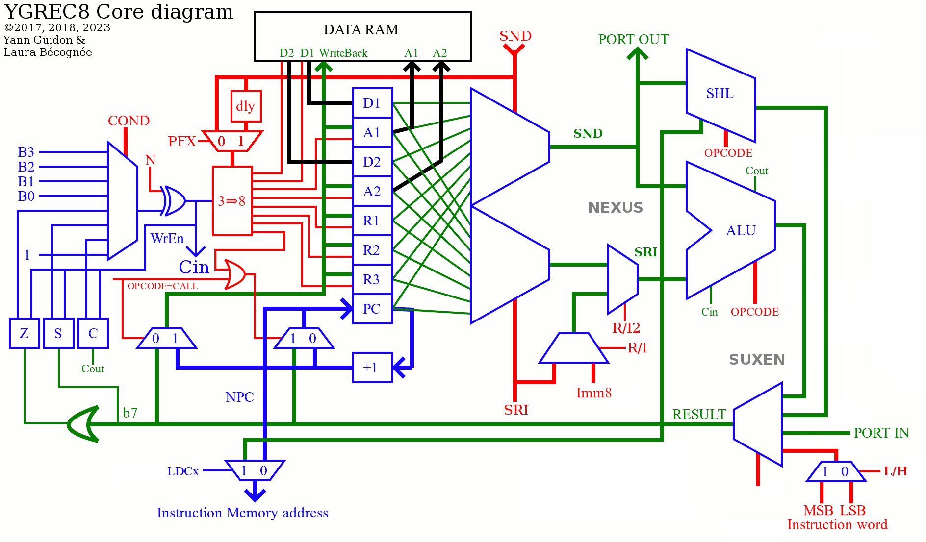
The state of the YGREC8 core is represented by the A1, A2, R1, R2, R3 and PC registers, as well as the three Status flags C, S and Z. Of course, this excludes the memories (instructions and data) as well as all the I/O space registers (some could store bank numbers) but here I focus on the core.
The three flags take three bits and that fits in a byte, with 5 bits left. With the new PF opcode, this free space is now totally used:
One bit is set when the current opcode of PF. This will be cleared by the next instruction, which will start by looking at this flag to modify its behaviour.
One bit will be new carry input, selected during the PF cycle by the condition field.
Three bits contain the real destination of the next instruction.
1+1+3+the existing flags equals 8, it fits nicely.
This matters not only for the simulator, but also because the core needs to handle interrupts and traps, which requires an accurate snapshot of the core that allows a precise restart.
There are some unused fields in the PF instructions, which might require more bytes to be stored for the next instruction.
What if you CALL using PC as SRI and another register as SND ?
SND gets PC+1 but PC will get PC, which ... yeah it wil get stuck. So we can detect this special case.
The result is that the next instruction's address will go into any other register, which is useful when starting a loop for example. So the corresponding opcode would be ENTER or ENTRY, useful when you don't want to compute addresses and your loop body has more than 8 instructions.
set R1 42 ; some loop counter

entry R2 ; sets R2 to PC+1

 ; do something long and useful here

  add -1 R1
  set R2 PC NZ
; end of loop
This looks nicer than
set $+1 R2
Now this increases the pressure on the registers. You could put the address on the stack top for example, but the loop counter would be better suited for this location, as it can be implicitly saved when a call occurs.
The address can be retrieved at the last moment:
set R1 42 ; some loop counter

loopentry:
 ; do something long and stupid here

  set loopentry R2
  add -1 R1
  set R2 PC NZ
; end of loop
The total code length is the same but the loop is slower by one instruction. It's not the highest code density ever, but it works.
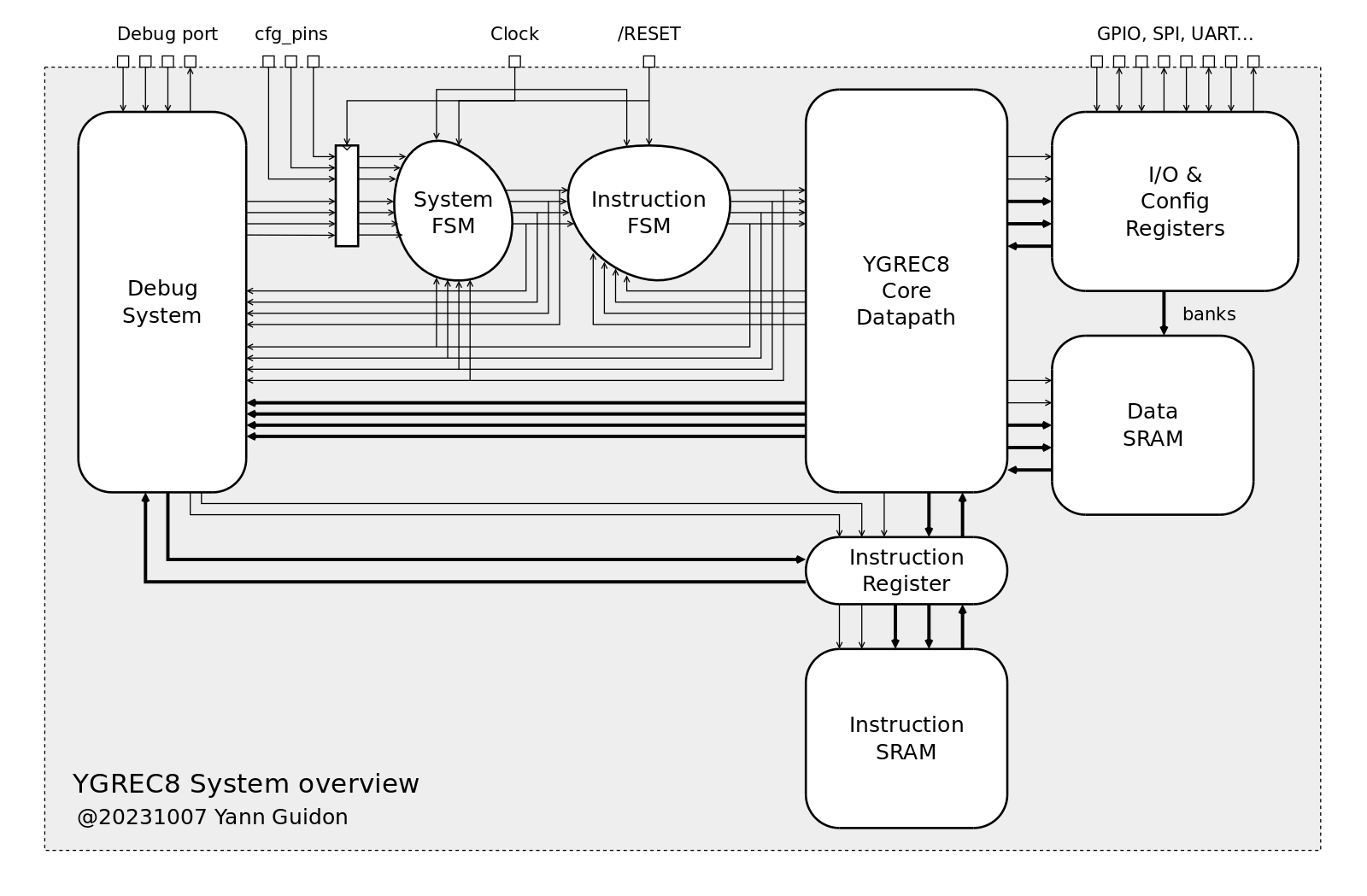
A complete YGREC8 system requires more than the main datapath. The following diagram shows the other necessary blocks :
The debug system is essential during development : this is the circuit that lets the developer write and read data inside the system. It can read and/or write :
the current instruction (read/write)
the result, SRI and SND (read only)
the flags (read only)
the current status of the core (read only)
From there, the developer can inject arbitrary instructions to access the other parts of the system (memory blocks, I/O etc.), dump or modify the state of the system... The debug circuits are totally asynchronous from the main clock, usually significantly slower. The developer must stop the core when inspecting or writing data. It is a bit more intrusive than other debug systems but it is designed to use as few transistors as possible.
The debug circuit has already been started as a standalone circuit but it could be replaced by anything that does the job, such as the Caravel harness used by eFabless (though it is much more complex and uses more real estate, meaning more prone to failure).
The core should be able to work in "standalone" mode, when no host controls the debug circuits. This is usually controlled by the state of some pins during /RESET : the System FSM can wait for a debugger to take control, or the FSM can load external instructions, either passively (as a SPI slave) or actively (by reading from an external SPI Flash chip). If the Y8 system has no internal code storage, you can bootstrap the core by sending 512 bytes through SPI (with an Arduino, RPi or ESP). The System FSM also handles the RESET/LOAD/START/STEP/STOP commands received from the debugger.
The Instruction FSM manages the lower-level details of scheduling the instructions and their details (such as OVL, HLT, LDCx, writes to PC...). This split of the FSM greatly simplifies the design and the modularity. More states are added as more features and corner cases are developed. Meanwhile, the System FSM remains core-agnostic.
The Y8 core does most of the remaining work : decodes instructions, fetches operands, performs operations, write back the results and move things around... It reads instructions from the Instruction Register, which usually transparently interfaces the Instruction SRAM. The instruction can also be read or written by the debug circuit, for inspection, injection as well as for writing a new program or overlay into the Instruction SRAM.
The Data SRAM is a plain memory array. 2 areas of 256 bytes each do the trick but some banking could take place if needed and if the necessary resources are available.
The IO & Config Registers is a user-defined area of 512 bytes that does everything that the rest can't. This is usually where customisation takes place, signals enter or exit the system, default behaviours are configured...
...
Still missing : the interrupt controller. Stay tuned.
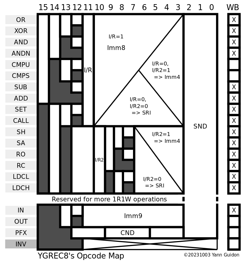
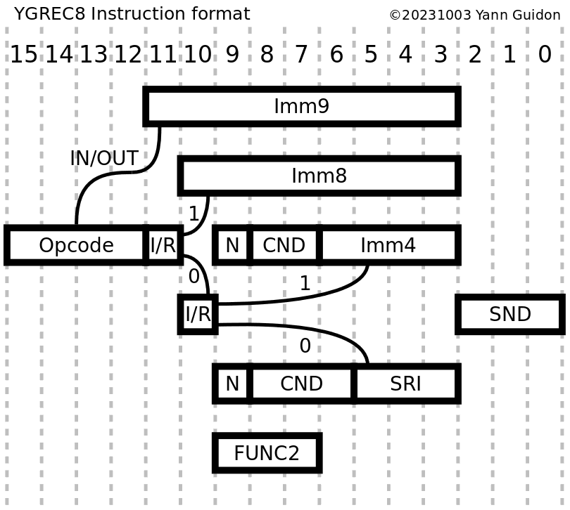
As I review and refresh the documentation, I realise that the pressure on the opcode map can be reduced a bit. There is a new prefix opcode (that interacts with the FSM) but the extra/optional opcodes do not need the conditional/predication bits. This would move a whole block of opcodes to lower bits and free more room. The prefix would have its own opcode and INV will remain untouched. Some reorganisation is required as I refresh the doc...
SH/SA/RO/RC are 4 optional opcodes that would now be located in the CND field, which is 3 bits wide. This leave 4 more opcodes, maybe for multiplication or whatever. But this frees 3 more main opcodes !
Maybe LDCL and LDCH could have a 8-bit version though that would be pointless (a SET Imm8 Reg instruction would do the same).
IN and OUT would have their own main opcode root code, not straddling across bit boundaries
...............
Update :
Here are the new versions of the opcode map and instruction format:
There is now ample room for more opcodes in the future, though they do not seem required now. There is also a separate prefix opcode, a totally independent INV opcode, and IN and OUT have the same opcode binary prefix (unlike previously).
The PFX opcode uses only the CND and SND fields, more could be used later. It doesn't check the I/R and I/R2 fields... yet. They should be kept cleared so far. More prefixes could appear in the future, for example using the SRI field.
I know : this will force me to rewire the mechanical assembler... The VHDL assembler will also need some revamp.
The core diagram has been updated too, implementing the prefix opcode: the output of the condition selector can be routed to the carry input of the ALU on the next cycle, and the writeback address can be delayed so write occurs on the register designated by the prefix and not the current instruction.
Maybe later : CMPU & CMPS can be dropped by adding 2 flags to the prefix : one to prevent result writeback, another to treat operands as signed. This would enable tests using the boolean opcodes.
 Yann Guidon / YGDES