JasMoH
-
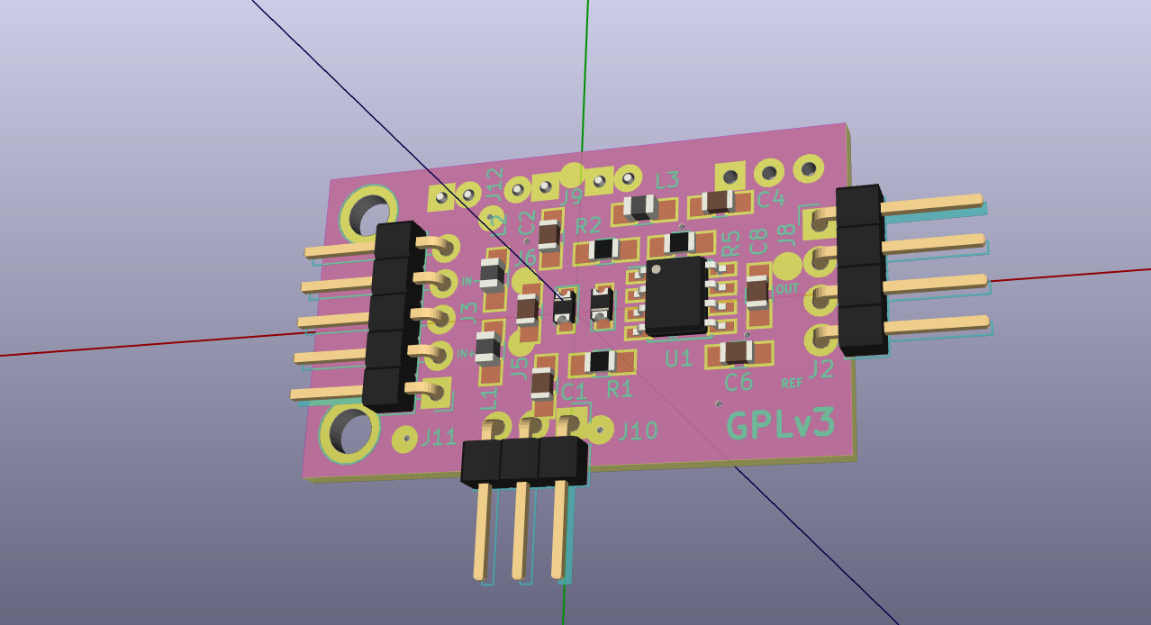
PLL Debug
01/09/2018 at 20:43 • 0 commentsBack from the holidays, and back into the swing of things. This post is rather rough because I don't feel like cleaning up my personal notes, but here's some raw, unfiltered black tar debugging. as always, the TL;DR is I'm an idiot who can't read letters...
Double check your footprints kiddos!
Pll testing notes:
Initial checkout:
Input midpoint tracker works at a variety of frequency down to the 10HZ range - coo.
Comparator is not comparatoring - uncool.
I’m thinking that this is a hysterisis problem. Pull up r88 - consider new values for r87
and r88 - or remove entirely and use on board hysterisis (dpending on low freq. performance?)
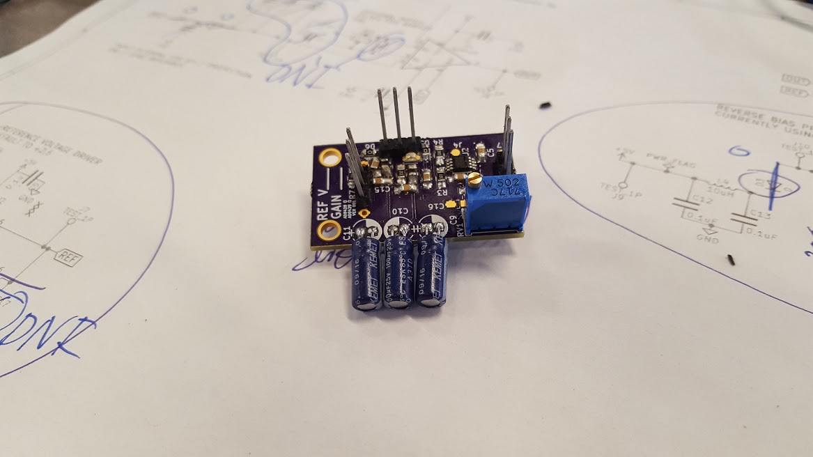
Pulled off r88 (feedback resistor). In process noticed issues with solder bridges on comp. Pins.
It has worked intermittently, but appears to have issues w/ manufacturing (wrong footprint).
That was an ordering problem. I ordered sc70 (.65 pitch) package - i laid out sot-23 (.95)
Next time: include nicer grounding studs for scope probes!
1/8/18
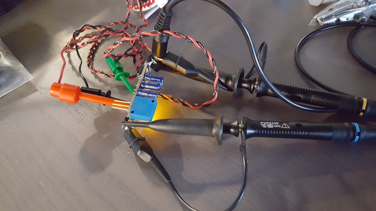
Replaced comparator with correctly packeged part. Always fun to do smt rework with my heated screwdriver soldering iron...
Midpoint tracking issues -
Seem to have issues with the input midponit tracking, even on 1KHz. Unsure why that was working before but not now.
measured 3v3 at non-inverting input (about 10x), and railing at output. Colud this be due to tolarance issues w/ rc?
Quick’n’dirty spice-y sims say that it shouldn’t be that sensativ eat 1k (20% mismatch between the input and output)
Op amp damage?
Loading effects from comp?
5000 rA input bias current, 10^13 input resistance. Should be good fine.
Op amp lifted off due to incorrect footprint sizing. Likely under stress… fix that and try agin...
1/9/18
Repaired input midpoint tracking opamp (u7) and it works again. So that’s cool.
Still no PLL lock though. Comparator is just railing out...
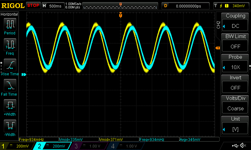
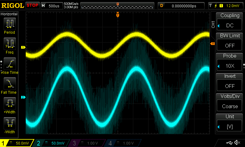
Quick midpoint characterization. “Decent” at 10 Hz, falls appart in the single Hz range.
This should be good enough for a first pass, it’s unlikely to ever be used bellow 20Hz due to 1/f noise.
Sceenshots:
I bought the wrong footprint. Fucking again. I am not a clever man
-
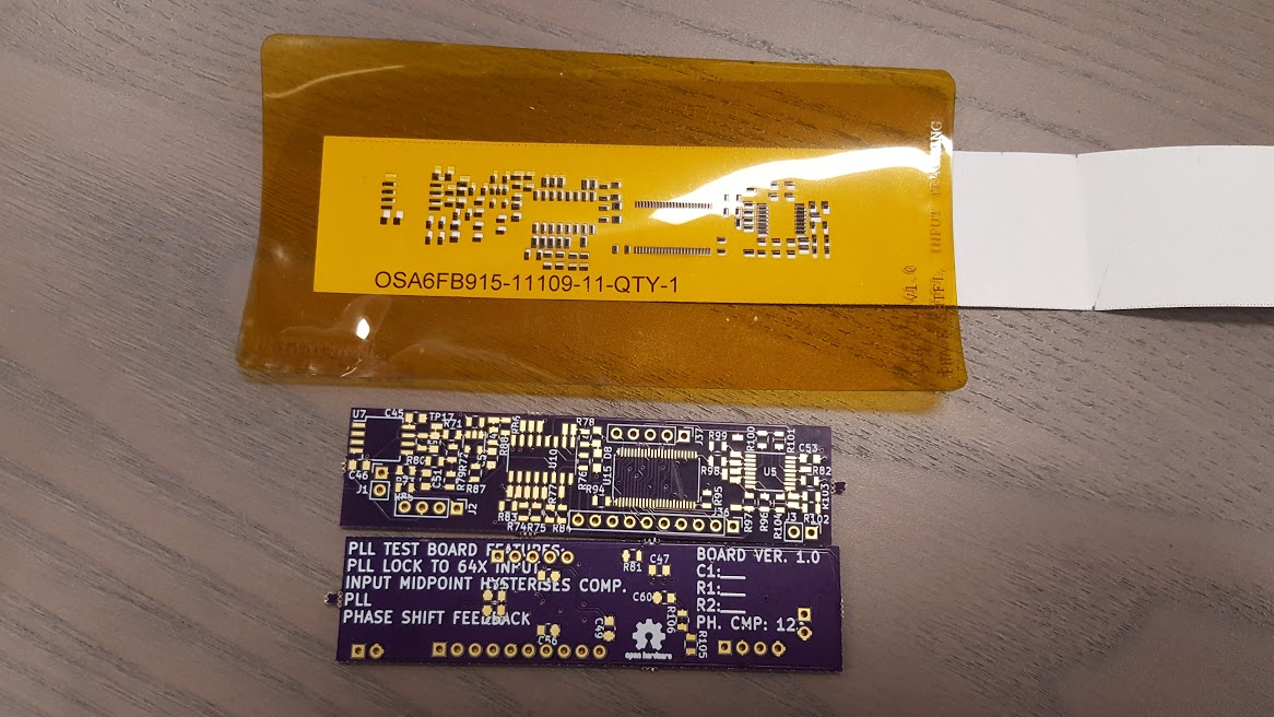
PLL prototype test board in
12/26/2017 at 22:32 • 0 commentsPrototype board and top solder stencil for PLL. The design goals are
support ~1Hz - 100kHz input frequency
"arbitrary" waveform that is between +-5V and crosses its midpoint twice per cycle.
outputs 64x the input frequency for the ADA2200 demodulator
phase shifts output to allow manual phase adjustment.
I'll be populating and testing this out in the next few days. I may decide to OBE the phase shifter in favor of just having 2x ADA2200, and support I and Q demodulation and digital phase shifting.
-
PLL test board ordered - LNA board started
12/15/2017 at 00:31 • 0 commentsTest boards and stencils for the PLL subsystem are on order. This includes a CD4046 based design with divide by 64 capability for the ADA2200's clocking requirement. It also can phase shift the output by steps using a digital delay line in the feedback loop.
The input conditioning logic will track the midpoint of the input clock and use that as the reference for a comparator. This should allow flexible inputs from the "real world".
![]()
I've also begun laying out the front-end, which has by far the most stringent layout requirements. Both the transimpedance amplifier (pictured), and the instrumentation amplifier require guard rings for mitigating stray surface charge migration. I have both of them under their own cans.
![]()
-
Initial Design Review
12/07/2017 at 21:50 • 0 commentsI have the initial schematic for the analog front end done! I'm currently soliciting design reviews from basically everybody I know.
See the design here: https://github.com/JasMoH/Photoacoustic/tree/DR1/lock_in_amplifier
![]()
![]()
![]()
![]()
![]()
![]()
-
Another Weekly Status Update
12/04/2017 at 20:30 • 0 commentsProgress from last week:
LNA and transimpedance amplifier schematic complete
Power supply complete
Initial high gain amplifier design complete. Gain selection scheme complete.
Selected mechanical switches for user input.
ADA2200 added, input protection and indication created.
Connector scheme complete
RF can for LNA selected
Design for manufacture/test begun. (test point addition, 0 ohm resistors to isolate or modify circuit, resistor / capacitor component minimization).
Found some real cute 0603 smt test points that’ll let me sprinkle tones of TPs without taking up too much board space for down the line debugging.
Outstanding todo:
PLL - find/ implement/ build. It’s looking like I’ll need to do at least some signal conditioning on the front to accommodate flexible input signals, and may need to build large portions of it due to low frequency range
Line filter - choose a 60Hz line filter implementation. It’s for sure going to be put at the input to the high gain amplifier chain, after the LNA. Debating stand alone active filter, integrating into the high gain amp, others.
Op amp selection review - I have some “lazy” op amp choices. I’m currently using the OP1177 as a “performance” amplifier and the lm358 as the “cheapo” amplifier. The OP1177 is expensive (~$2.50), and the lm358 is kinda crap (1.1MHz GBWP). I’m adding a lot more op amp applications than expected. These include: reference voltage buffer, guard trace driver, and amp overload indicator. I expect that I may need a few more to complete the design, such as an active line filter. I would like to get a cheaper “performance” amp and a better “cheapo” amp than my current selection.. I’m considering the lm833, which is similar in price to the lm358 and has similar performance numbers (GBWP, input noise) to the OP1177.
Select power connector: just something cheap, dual supply (+-12V), and polarized so it can’t be inserted backwards...
Design for test / manufacture:
Sprinkle more test points
Add 0 ohm resistors for isolating subcircuits, adding flexibility, etc.
-
Shopping for PLLs and Transimpedance Amplifiers
11/29/2017 at 13:40 • 0 commentsI have completed the schematic for the power supply and filtering system. I have a first pass at the amplifier chain design, at least for single endend and differential voltage inputs.
Many lock in amplifiers include a transimpedance amplifier to make current measurements, for instance with photodiodes. From looking at some demonstrations on youtube (link below), many of these units are capable of femptoAmp sensitivities. I'm currently shopping for a transimpedance amplifier design with sufficiently low noise to support these measurements.
I am also looking for a PLL system for the demodulator. I'm using the ADA2200, which requires a reference clock at 64x the modulating frequency. So I'm looking for a PLL that will lock at low frequency; Ideally down to 10Hz or less for maximum flexibility, but 100Hz is probably more realistic due to flicker noise.
-
Lock In Amp TODO
11/27/2017 at 16:34 • 0 commentsI've been letting this project lie fallow for the last couple weeks. I intend on getting a dedicated lock in amplifier board built. here is the todo list for that effort.
- Characterize components:
- Put up a resistor / pot bridge, see what sensitivity we get and whatnot…
- Just do the lock in portion.
- Add back in pre-amp - don’t worry ‘bout rail protection for today - monitor
- Change midpoint resistors!
- See if ad8429 works with shorted Rg for 10,000x gain? Should be like 0.6 ohm (check math)?
- Possible re-design of input amp?
- Work noise budget!
- Test point selection
- 100 mil header
- 0603 probe pads - https://www.digikey.com/product-detail/en/te-connectivity-amp-connectors/RCT-0C/A106144CT-ND/3477801
- Get rid of ground pigtails somehow?
- Mmcx connectors - $$$
- Connector selection
- BNC - edge mount
- SMA - edge mount
- 100 mil headers
- Guard traces
- Possibly a can? Pick an optional can and footprint.
- https://www.digikey.com/product-detail/en/leader-tech-inc/SMS-201C/1798-1176-ND/7203462
- Transimpedance amp w/ switches for single ended, differential, and current inputs
- Component selection
- Switches - spdt
- Switched gain
- common numbers for measurement (1x one of the amps)
- Switch selection
- 2xN 100 mil header jumpers
- N pole N throw slide switch - $$$? Real estate?
- DIP
- amp cascade - LNA + “normal” amp
- Nominal goal for 1 nV sensitivity with long enough time base; 1nV -> ~1V
- 1e9 v/v system gain.
- Ad8429 does 1e4 v/v, leaving 1e5 remaining
- Run noise budget trade; friis.
- 1e2 + 1e3 cascade (order)
- 1e4 , 1e1 cascade?
- Run LNA at lower gain (i.e. 1e3 for each stage?)
- Datasheet + friis to make trade
- Multiple 1e3 stages would be more user friendly. Just a chain of amps w/ a single switch to enable (1e3 v/v) or disable (1 v/v).
- Noise budget for additional esd protection at input?
- Diode noise acceptable?
- Or just not do it and label as esd sensitive? Cheap enough components to blow...
- LNA selection
- Reason not to pick AD8429?
- Secondary amp selection
- PLL w/ divide for lock in?
- F, 2F modes
- PLL lock / unlock indicator LED
- Component selection, again...
- Line filter at input - concerns with saturation
- Switched enable - dip or jumper
- Power supply
- LDO selection, +5, -5, +3v3? Unless others necessary
- 7805 serries
- others
- Line filter - maybe?
- Pi filters from current design should be good.
- Beef up bulk caps
- Move indicator diodes to clean side of supply
- Reverse bias protection w/ fets - clean side / dirty side?
- Supply connector w/ bias protection
- Output integration / lpf
- Switched time constant / output buffer
- Long time constants (~10s) desireable
- Output monitor connectors
- Amplified signal
- Demodulated signal, I/Q components
- LPF output
- Phase shifters - include or not?
- How to even implement?
- Indicators, dials, connectors, etc. start pretending at being a “real instrument”
-
Amplifier Initial Functional test
11/09/2017 at 22:24 • 0 commentsAfter tweaking my solder setup, I got one of my three prototype boards to work. This one is populated with the AD8429 (variable gain amplifier) and a trip pot so I can get an idea for the gain necessary for my application.
![]()
My totally low noise haywire setup. PC sound card on lowest volume stimulating a 440Hz sine wave for input.
![]()
Results with a low gain applied.
-
Amplifier Boards In
11/07/2017 at 19:31 • 0 comments![]()
![]()
Boards and components have arrived. thanks to the good people at mram I have the miscellaneous cables 'n' things that I forgot.
Power filtering and reference voltage driver circuit passed smoke test and initial functional test, so that's nice. I have a soldering defect somewhere on the signal side, so now it's rework time!
-
Instrumentation Amplifier Prototype to Fab
10/27/2017 at 22:23 • 0 commentsSent out PCB to OSHpark, have parts on order. simple board to breakout the AD842x, add reference voltage. has enough lands for passives to permit flexible notch filters / gain adjustment / RFI filtration, and the like.
![]()
Photo-acoustic Spectroscopy
Creating an at home photo-acoustic spectroscopy system