Close
0%
0%

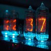
One Tube Nixie Clock

It is time to take my nixie hardware testbed from the breadboard stage to something that doesn't have wires sprouting everywhere.

Similar projects worth following
A while back, when I decided that I wanted to make my own Nixie clock hardware, I created a testbed to work through my various options. While I was doing this, I was also busy buying Nixie tubes and I created a bunch of adapters for them to plug in to this testbed so that I could admire them before I actually got around to building a clock for them.

Well, the testbed has served its purpose, but I use it constantly to display a one-tube-clock, swapping different tubes in and out. So I thought it was time that I actually built some real hardware that was a little more presentable.

The clock will run off a USB port, synchronize time via the internet, be configurable via a web browser and use my adapters to allow me to swap different tubes in and out.

Features include:

STCBOM.csv

BOM

Comma-Separated Values - 3.22 kB - 02/04/2018 at 18:44

Download

USB-UART-USB-UART.pdf

USB-UART sub-schema

Adobe Portable Document Format - 44.36 kB - 12/21/2017 at 02:41

Preview

HVPS_SMD-HVPS_SMD.pdf

HVPS sub-schema

Adobe Portable Document Format - 32.03 kB - 12/21/2017 at 02:41

Preview

ESP8285-ESP8285.pdf

ESP8285 sub-schema

Adobe Portable Document Format - 41.87 kB - 12/21/2017 at 02:41

Preview

OneTubeClock.pdf

Main sheet of design

Adobe Portable Document Format - 51.53 kB - 12/21/2017 at 02:38

Preview

View all 6 files

  • Notes and Thoughts

    Paul Andrews01/25/2018 at 03:22 0 comments

    Some Thoughts on the Next Version

    Its great as it is, but here are what I would put in the next version:

    A LiPo battery

    I want to be able to carry this thing around from one place to another. It would be optional and just plugin in underneath the main board. I would need to add a boost converter from 3.7V - I need 5V for some of the logic. The power supply itself could run straight from the 3.7V. It would need to charge when plugged into a USB port.

    So I guess I won't be dismantling my testbed just yet.

    Fifteen HV Pins

    I pull 12 HV pins out currently (plus another two for the little neon indicators). This is so I can drive tubes that have one or two decimal points. However there is a tube called the B7971 that is a 15 segment neon display. It is big. I can't drive it using this clock :-(. On the current connector I have one unused pin, so I would just need to add another two. In other words, instead of a 2x8, I would use a 2x9. That is a small change.

    Real Time Clock

    Currently it just syncs with the internet. But if I want to use it somewhere were I can't connect it to the internet, like my office, I need some other way of keeping the time. Actually I could add this now via the I2C expansion header, so maybe I don't need to add special support after all.

    A Button

    If I don't have access to the internet, I need some way of setting the time. Again, I could add this via the I2C expansion header. So maybe, I need to design a little add-on module for use away from the internet.

    Hardware Notes

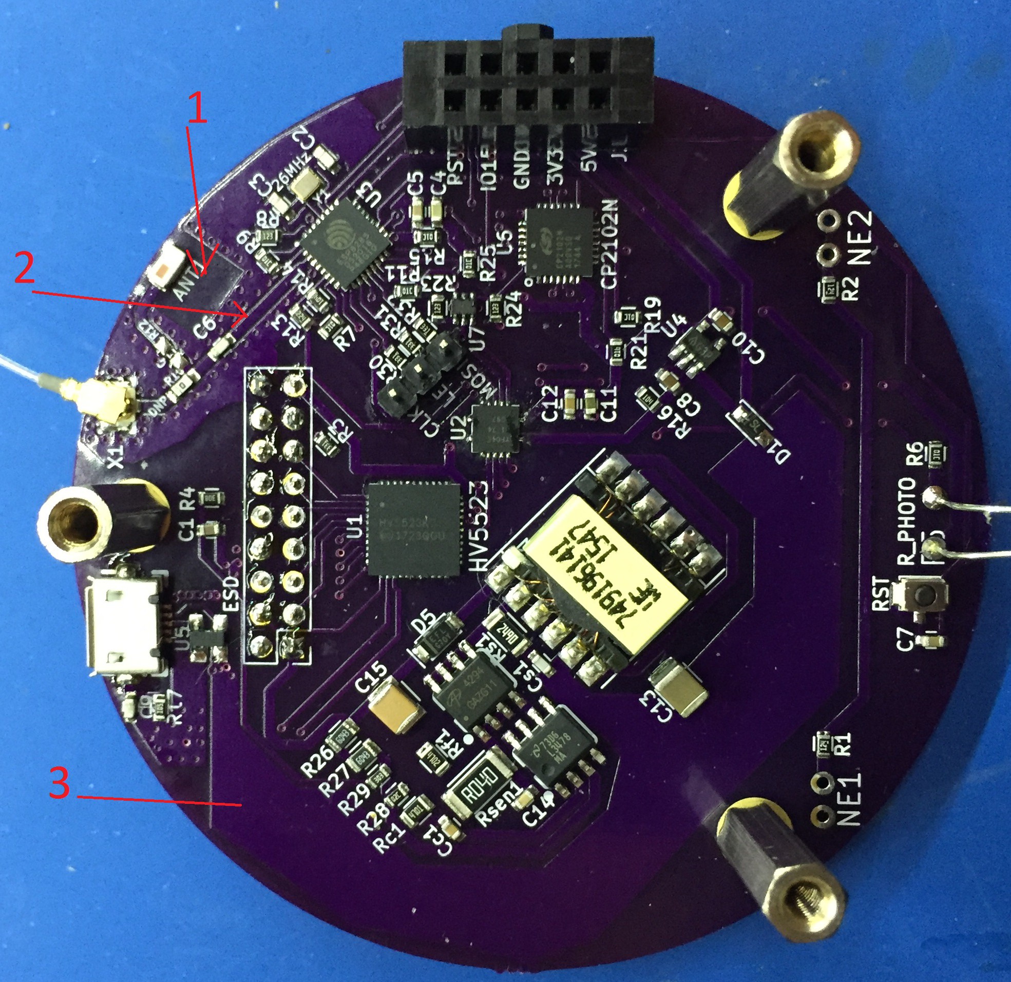
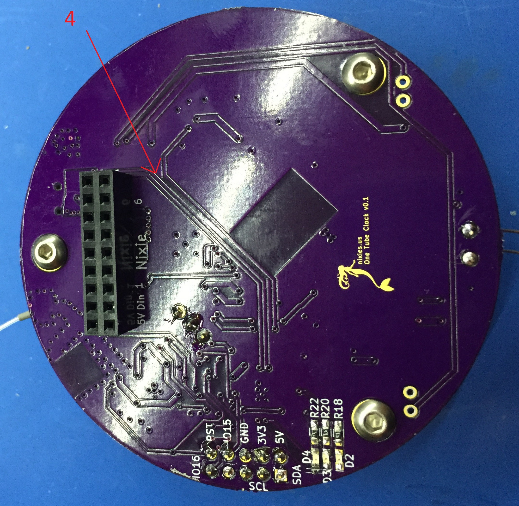
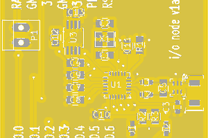
    There are some not-so-obvious but important points about the PCB layout:

    1. The layout of the copper layer here (on both sides of the board) is defined by the manufacturer of the specific chip antenna. 
    2. This is a 50 Ohm trace that leads from the ESP8285 to the antenna. The width is chosen specifically to match the copper depth and the characteristics of the substrate. KiCAD has tools that help to calculate this width given this information. OSHPark has the information needed to make this calculation. If you use a different fabricator, or a different spec board from OSHPark, you should re-do this trace. Though I am not sure how important it really is. On the flip side of this trace is an unbroken ground plane. No other traces can cross this trace underneath it.
    3. This +5V plane is kept as wide as possible to minimize resistance and hence minimize voltage drop when we start to pull more power.

    You'll note that there are also many through-vias around the antenna traces with ground planes both top and bottom. This is to minimize stray EM radiation.

    This pair of traces are the USB data lines. They should really be a differential pair. Like the antenna trace, the impedance is important, but here layout is also important. I kept them parallel, but that was about it. The CP2102N is a full speed device. We shouldn't really need to worry until the traces get up to about six inches in length.

    Software Notes

    I'm pushing it with the ESPxxxx devices. I was careful to test out my code before I committed to using them. The problem is that the WiFi gets priority over everything else, so anything that is sensitive to timing can get thrown out. This is particularly important for the NeoPixels, which use a clockless protocol. In fact at one point I updated my ESP8266 Arduino libraries to v2.4.0, and the NeoPixels started glitching on me. Down-graded back to v2.3.0, and all is well - there is still a chance they will glitch, but I haven't noticed it in all the months I have been using it.

    Allegedly the ESP32 would be better in this regard - it has a separate core for the networking.

  • Build

    Paul Andrews01/22/2018 at 03:14 0 comments

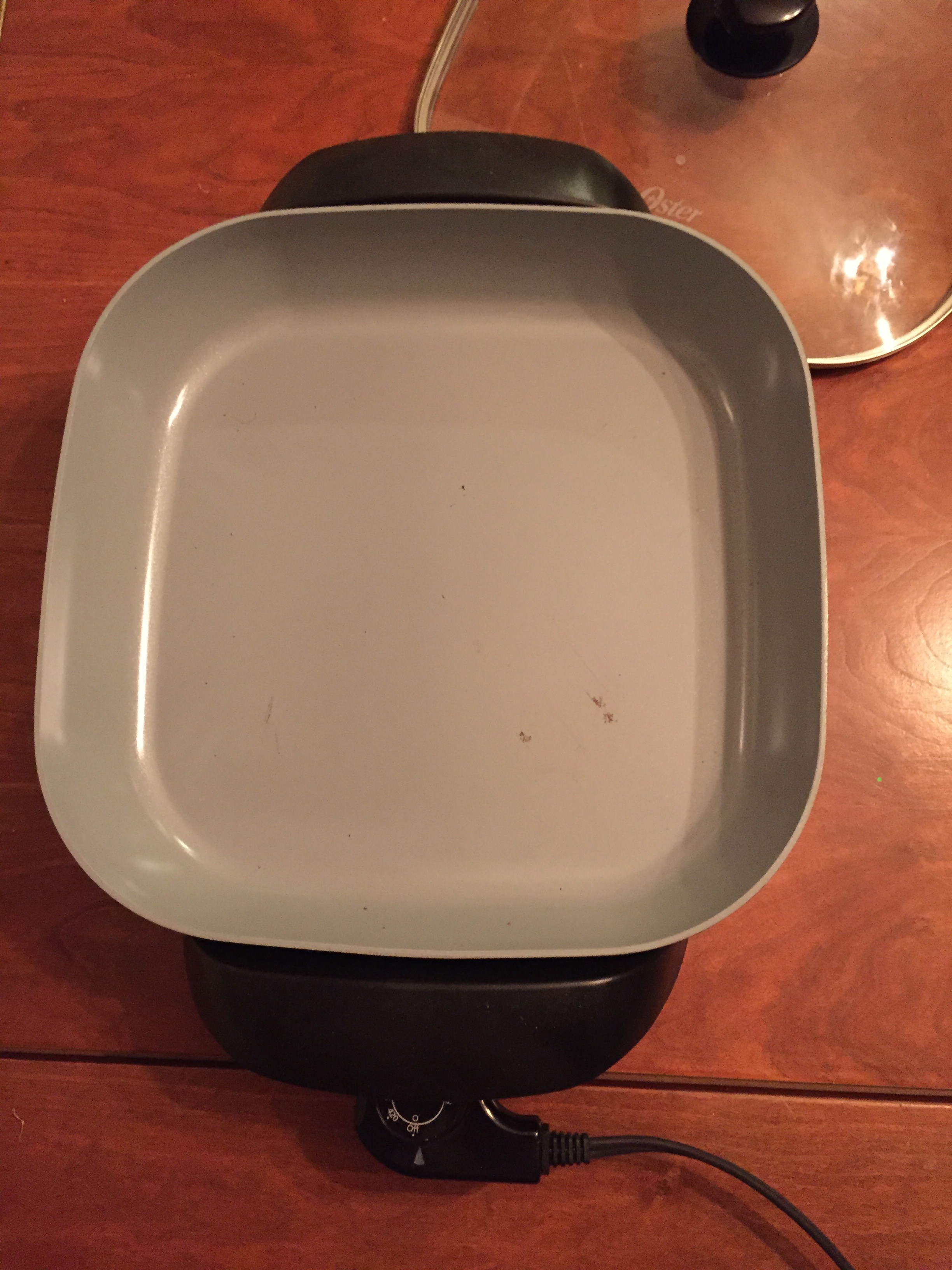
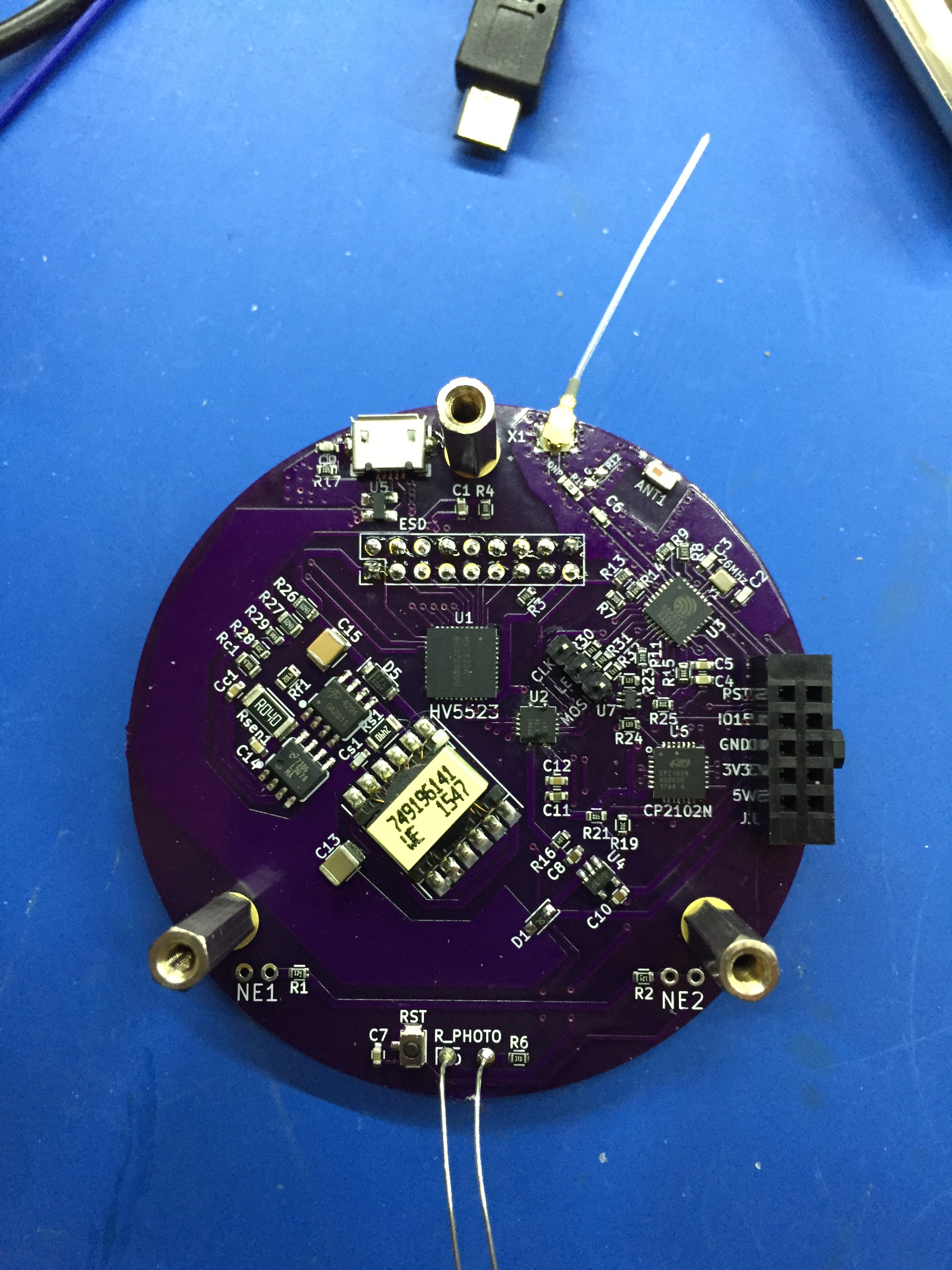
    I finally had time to get around to building one of my clocks. I spent an hour or so labelling all the component bags so I wouldn't be searching for components once I had the solder paste applied. Then I taped the board to my bench and used the stencil I had made at OSHStencils.com to apply solder paste. Once done I started adding the components to the board and finally wandered over to my reflow soldering station:

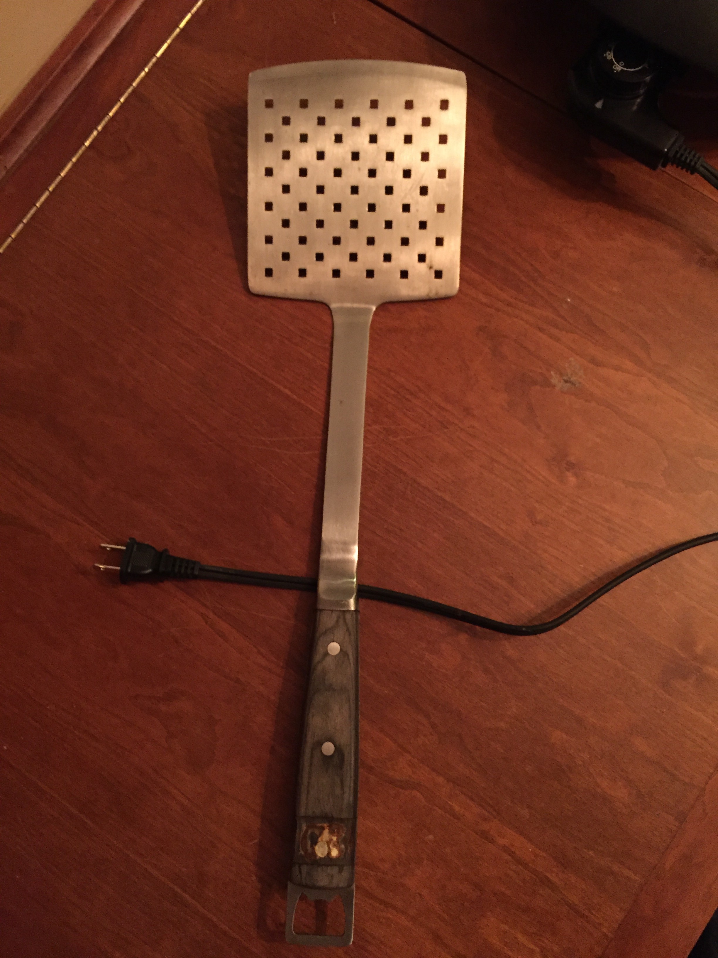
    Yes. Its an electric griddle. About $40 from Target. As this board was bigger than all the others I had made, I needed a special tool to load it into the griddle:

    I knew that over-sized spatula would come in handy one day.

    Anyway, this is what I ended up with:

    Testing went surprisingly smoothly (at first):

    • My PC recognized the board when I plugged it in
    • I could configure the CP2102N USB-UART chip using Silicon Labs config tool
    • I uploaded the clock program and assets to the ESP8285 (U3 in the picture above)
    • My phone saw the access point presented by the ESP8285
    • I could run the web GUI

    Then I plugged a tube in and things weren't as I expected: All of the digits were lit up and the LED backlight wasn't! There followed about 2 hours of debugging. First, I hooked up the Clk and MOSI pins to my oscilloscope - they showed that the ESP8285 was producing the right signals for the HV5523. However, the signals are level-shifted through a TXS0104 - I very carefully managed to stick the probe on the output side, and there was nothing. So that was it. I spent an hour or so trying to touch up the contacts with my soldering iron and eventually I succeeded! One or other of the +5V or 3V3 connections had been bad (note to self: Don't put vias on really small pads!). Now I could see the clock displaying digits, except that it was displaying all but one of the digits - in other words it was inverting the outputs. I took a look at the schematic and for some reason I had tied the HV5523 polarity pin to ground rather than +5V. Fortunately, this was easy to fix in software, and finally I had a functioning clock:

    If you're wondering, the dangling thing on the wires sticking out the front is a LDR - at some point I will be putting this in a case, so I didn't want to trim the wires until then.

    There is one other problem with the hardware: I should have cut a notch in the PCB where USB connector is, without it it is pushed up at an angle by a lip on the connector, however it still works.

    I like these things so much that I can't wait to assemble my other two boards and scatter them around the house. Unlike a full 6-digit clock, they easily fit anywhere.

    When I get a bit more time, I will add upload all the CAD files and source code to GitHub and add links to everything.

  • The Boards Have Arrived!

    Paul Andrews01/09/2018 at 01:43 2 comments

    The boards have arrived! Unfortunately it is going to be a couple of weeks before I get to do anything with them. While I was waiting, I was honing the software, which is pretty much ready to go.

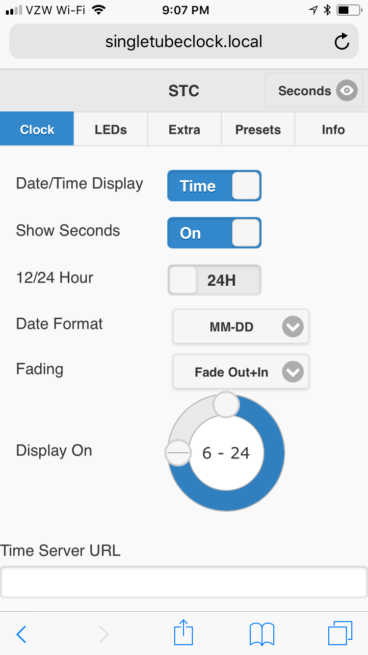
    Here are some screen-shots from the web GUI. The Clock screen lets you configure all of the actual time display features.

    The Time Server URL is used to synchronize the time with NTP and adjust for timezone and DST - I blanked it out in this image:

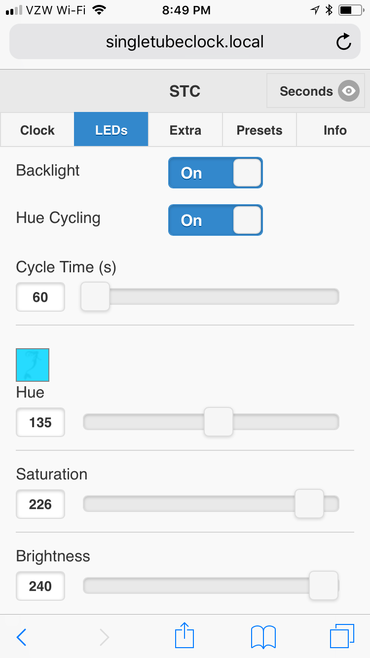
    The LEDs screen allows you to control the backlight and reflects the current state of the backlight in real time using web sockets push from the clock.

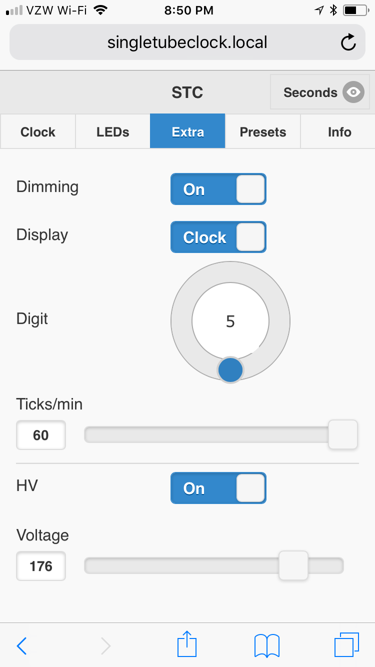
    The Extra screen allows you to change the purpose of the hardware:

    • You can use it as a clock.
    • You can also use it as a tube-tester by getting it to just cycle through all of the digits.
    • Finally you can use it to de-poison the cathodes by increasing the voltage and having it cycle through all of the digits slowly enough for the over-current to burn off the deposits from the cathodes. Or, I have some tubes in my collection that just need to be run at a higher voltage.

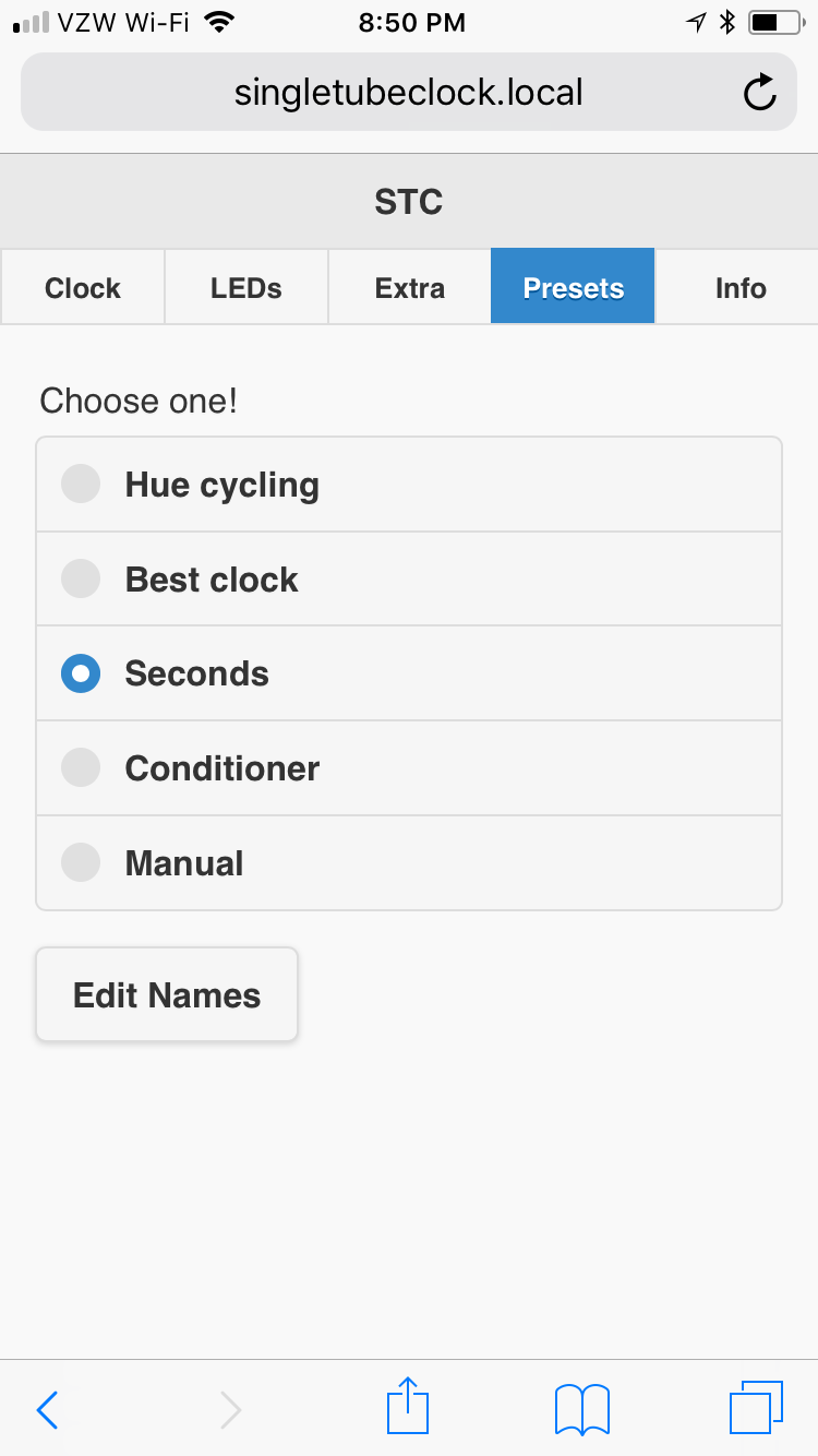
    There are so many options that it comes with five presets that you can just jump between. If you make changes to a preset, they are saved automatically, and you can rename the presets.

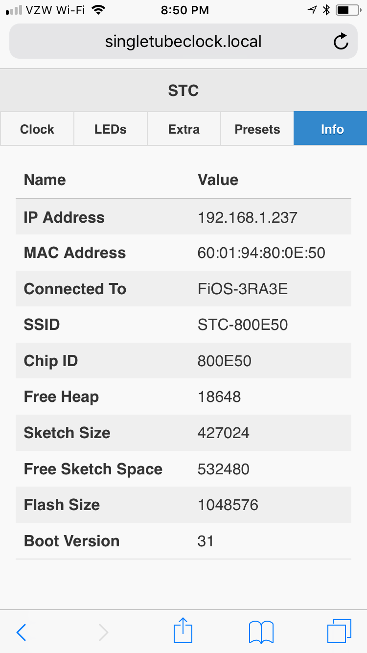
    Finally, there is an info screen:

  • Prototype at OSHPark

    Paul Andrews12/21/2017 at 02:47 1 comment

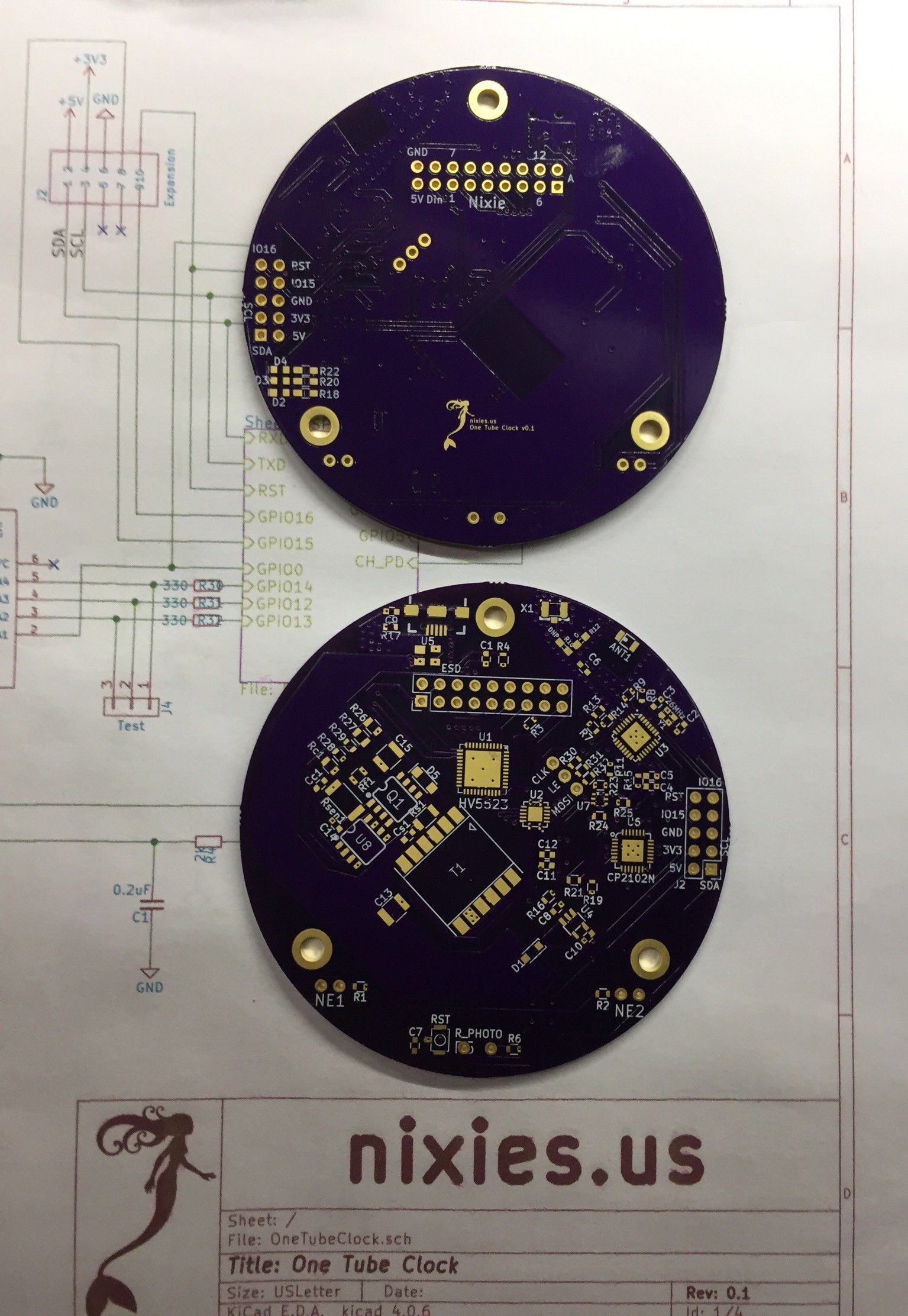
    Well, my prototype is being fabbed by OSHPark, along with a stencil from OSHStencils!

    I also designed a couple of adapter boards. One for an IN-12, because I test everything with these tubes. This is a vertically mounted board. One for an IN-18, because I wanted to make a horizontal adapter and I also need an adapter for those tubes.

    So, fingers crossed that I didn't make any mistakes in the design and layout, and that I can actually build it without messing it up!

    I uploaded the OSHPark render and the schematics for the design.

  • Progress

    Paul Andrews12/12/2017 at 15:03 0 comments

    I am waiting for some parts to arrive before I can start laying out the board. The design is basically done, except for some tweaking I have been doing for things such as power sources, connector layouts, pin breakouts etc.

    In the meantime I have been polishing the software using my breadboard prototype. Here are some of the things I think are worth sharing:

    Development Framework

    As you probably know, I am using an ESP8285 - this is an ESP8266 with 1M of on-board flash - so it reduces component count and frees up a couple of extra GPIOs. I use the ESP8266 arduino development framework. A good resource on this framework is the ESP8266 Arduino Core docs. The arduino development framework is kind of like the Java of the hardware world. It has many, many libraries that a developer can leverage, rather than having to roll their own for every different processor out there. Developing for this framework also means that my own code is more portable.

    The ESP8266 boards are fully supported in the Arduino IDE, however I use Sloeber- an Arduino Eclipse plugin. It makes me way more productive.

    Key Libraries

    From the outset my aim was to leverage the WiFi connectivity of the ESP boards. I have developed a web interface for Nixie clocks before, and I used the ESPAsyncTCP library, rather than the libraries from the ESP8266 core for Arduino. In particular ESPAsyncWebServer. I wrote a small ESPAsyncHttpClient to go with it. Asynchronous communication places less load on the ESP8266 - it allows it to get on with other tasks, while the communication is happening in the background. I came across this library via fauxmoESP - a library that allows you to mimic WeMo devices, so you can control things using Alexa - it uses the ESPAsyncTCP library!

    One problem that needs to be solved when using WiFi is the initial connection to a router. I had previously rolled my own solution to this before, but it is a finicky business and after I had implemented it I came across WiFiManager, which displays a captive portal when a device tries to connect to the ESP, and allows you to choose which router you want to connect to. However, it uses the synchronous web server and I wanted to use the asynchronous web server. Fotunately someone had already implemented that too: AsyncWiFiManager

    Interrupt Handling

    I implement various fading effects by turning power on and off rapidly to selected digits. I do this using interrupts to guarantee the timing - the ESP8285 has many other things to do, so the loop() method isn't called at consistent enough intervals to rely on that for timing. I had implemented this a long time ago using timer0 - the handler issued SPI calls (using the Arduino SPI library) to set the state of the HV5523, telling it which digits should be on and which should be off.

    It all worked fine until I integrated the ASyncWifiManager and started serving up web pages. Then it started crashing randomly. When the ESP does that it spits out a stack dump as a bunch of numbers, so the first thing to do was to convert these to symbols. If you're using the Arduino IDE there is the EspExceptionDecoder for doing that. For me, I needed to use the EspStackTraceDecoder command line tool.

    What it told me was that I was always crashing with an illegal instruction error. WTH? After some googling I found that various system calls can cause flash to be unmapped from the address space. If an interrupt happens at that time, you will get an illegal instruction error. The solution is to move your interrupt handler to RAM using the ICACHE_RAM_ATTR tag. For example:

    void ICACHE_RAM_ATTR myHandler() {
    // Do some stuff
    }

    However:

    1. Everything that is called from that interrupt handler also has to be in RAM.
    2. There isn't much RAM.
    3. SPI methods are not declared with that tag, so they are all in flash.
    4. There isn't much RAM (see 3).

    So. I created my own copy of the SPI library and added ICACHE_RAM_ATTR...

    Read more »

  • ESP8285 GPIO

    Paul Andrews11/26/2017 at 02:10 0 comments

    Theoretically the ESP8285 has 17 GPIO pins and one ADC pin. The bad news is that many of these are already assigned to specific functions. Some of them are still usable, with restrictions, some aren't usable at all.

    First here are GPIO states for various boot modes:

    GPIO0GPIO2GPIO15
    Normal startup110
    Programming010
    Boot from SD001

    Because these pins have to be in a specific state at startup, they can't be used as inputs. We also need to be aware that GPIO0 might change state if we are using it as an output - i.e., whatever hardware is connected to that pin needs to be able to handle that.

    After startup, we can do whatever we want with these pins.

    GPIO6, GPIO7, GPIO8 and GPIO11 are completely unuseable.

    GPIO16 is used by 'wake from deep sleep', and I would like to play with that.

    So, that leaves nine completely unused GPIO pins. We want the following pins:

    • MOSI
    • SCK
    • Latch Enable
    • Neopixel data
    • HV enable
    • HV adjust

    In addition, I want to play with USB charge detect, so I also want:

    • Charge enable
    • Charge 0 enable
    • Charge 1 enable

    That is all nine free pins. However I would also like, if possible to give access to I2C for expansion - that is an additional two pins.

    Fortunately, if we are careful, we can also use the three boot pins (GPIO0, GPIO2 and GPIO15).

    So, this is the plan:

    Pin FunctionRestrictionsClock Use
    0Boot mode selectCan't be used as an input. State during boot is dependent on boot mode.Neopixel data
    1TX0During boot, debug is output on this pin.SDA
    2Boot mode select/TX1Can't be used as an input. There is an external pull-up on this pin, so it also can't be used for applications that require Hi-Z (such as I2C).HV Enable
    3RX0During boot, while debug is being output on GPIO1, this is held high. So, if we use GPIO1 as SDA and this as SCL, no data will make it to any slaves.SCL
    4SDAThis is the default SDA pin, we moved I2C to GPIO1 and GPIO3 because it can handle the noise at boot, so it frees up this pin.HV Adjust
    5SCLThis is the default SCL pin. But we need it for, we moved I2C to GPIO1 and GPIO3 because it can handle the noise at boot, so it frees up this pin.CHRen
    6-8FlashOn the ESP8266 these are used to interact with the flash memory. Unfortunately, they are not freed up in the ESP8285.-
    9FlashOn the ESP8266, this is used for flash, but on the ESP8285 it is free. Yay!CHR1
    10FlashOn the ESP8266, this is used for flash, but on the ESP8285 it is free. Yay!CHR0
    11FlashStill not available on the ESP8285-
    12MISOSPI Master in/slave out. We don't need it for that...Latch Enable
    13MOSISPI Master out/slave inMOSI
    14SCKSPI clockSCK
    15Boot mode selectCan't be used as an input. There is an external pull-down on this pin.Free
    16Wake from sleepThis is used by the deep-sleep mechanism, should we want to use it.Free
    A0ADCThis is used for analog in. We attach a LDR to it.LDR

    By leaving two pins for I2C, I have an easy way to add more GPIO (including ADC) plus a whole host of peripherals like a little OLED screen for debug.

    All control of the clock will be via WiFi, including setting the time, so there is no immediate need to add buttons and switches, but I2C GPIO expansion could be used if more are needed.

  • Starting the Design

    Paul Andrews11/20/2017 at 15:57 0 comments

    Define Some Libraries

    Time to start putting some footprints and symbols together. My workflow for this is to define the device (symbol and footprint) in Eagle and then convert it to KiCAD using Eagle to KiCAD libs, to which I have contributed quite a few modifications. My main reason for this is that I use KiCAD for my circuit designs, but there are way more libraries for Eagle.

    I have two new parts I need libraries for (I already have libraries for everything else):

    • The HV5523
    • The TXS0104

    I couldn't find any existing Eagle libraries for these, so it was time to create my own.

    The first is a 7mm QFN-44 chip. I need to get that size right! In one of my earlier iterations of a USB-UART adapter, I didn't release that QFN-28 came in a couple of sizes and I fabricated some boards with the wrong size. Fortunately I found a footprint in an ST-Microelectronics library that I already had. I imported it into my own library and modified the size of the center tab to match the Microchip datasheet. Then I duplicated a symbol for the HV9808 that I had already defined, modified it a little for the HV5523 and hooked everything together.

    The second is a VQFN-14 - at least that is the version I will be using. I couldn't find this in any library I already had, but a quick search turned one up in SnapEDA. I downloaded it and imported it then checked the dimensions against the TXS1040 datasheet. It was a match, so then I quickly defined a symbol and hooked them up.

    Then I double-checked the dimensions, the connections and the pin directions. OK. Good to go, so convert it using Eagle to KiCAD libs and it is ready to use in KiCAD.

    Start the Board Design

    My board will use sub-circuits from other experimental boards I have already built (with a few modifications). Namely:

    • High voltage power supply
    • USB-UART
    • MCU

    I have never used hierarchical sheets in KiCAD before, but it seems like a good time to start. Coincidentally, it also seems like this is the only way to copy those sub-circuits into a new project with the version of KiCAD I have (4.0.6). Copy and paste just don't work. I followed the procedure outlined on this post by padu1000. I'll reproduce the text here, but it I have modified it slightly:

    • Copy "yourSchematic".sch from the original project to the new one. (At this point it will not show up in your kicad project)
    • In new project create a new hierarchical sheet with the same name as the one you just copied. You will see a popup that says this:
    • (A file named 'yourSchematic.sch' already exists. Do you want to create a sheet with the contents of this file?)
    • Click yes
    • Link up your libraries

    So now, just add the new symbols and wire them up to the sub-circuits :-)

  • Component Selection

    Paul Andrews11/16/2017 at 04:40 0 comments

    MCU

    Pretty early on, I had decided to try using an ESP8266 to drive all the functions of my clock designs. I had already used an ESP01 to provide network connectivity for an Arduino-based clock, and that had always seemed a bit like the tail wagging the dog. That is to say, the Arduino was a 16MHz, 32K device, while the ESP01 was a 64MHz, 1M device with built-in WiFi, yet the Arduino was doing all the work. One worry was that the ESP8266 would give priority to the WiFi functionality, which would mean that user code could be interrupted at any time to service possibly lengthy network tasks. The only way to find out was to actually try it, so I set about trying to find suitable dev boards. While I was doing that, I discovered the ESP8285 - a chip that combined the ESP8266 with 1M of on-board flash, meaning it was essentially a one-chip MCU solution.

    Dev Boards

    It was clear that this would be what I would aim to use, but in the meantime I needed some dev boards. I ended up with this shortlist:

    • Wemos D1 mini pro - this is an ESP8266 based board.
    • ESP8285 dev board - as the name suggests, this is an ESP828 based board
    • PSF-B85 - this is not a complete board, but is aimed at being soldered directly on to a main PCB.

    And more recently:

    • Seeed ESP-01M - this is a bit like the PSF-B85 in concept, except it is vertically oriented. This makes a lot of sense, because this puts the antenna in a better position.

    All boards have an on-board antenna, except the ESP8285 dev board.

    I bought them all, but I have several Wemos D1 mini pros that I use wherever I would normally use an Arduino. Again, in a finished PCB, I would aim to use an ESP8285 directly. Getting hold of these isn't straightforward, but you can get them on ebay.

    Proof-of-Concept

    Designing a board to directly use an ESP8285 (rather than one of the options presented above) is an interesting excercise, because you have to lay down tracks with specific RF properties, and pay attention to the placement of ground planes and through-vias. I had a couple of attempts at doing this, but wound up with this one on OSHPark.

    USB-UART

    Another important component is the USB port. If you are familiar with programming an ESP01, you'll know that you need a USB-UART board. Something like the Wemos D1 mini pro has one of these on board, so you can just plug it straight into a USB port for both power and programming. The Wemos also uses the NodeMCU mechanism to put the ESP8266 into program mode, so there is no fiddly holding down of buttons in some weird sequence.

    In addition to doing the USB to serial conversion, I wanted something that could detect the power mode of the USB port it was plugged in to. i.e. I wanted to know how much power I could get out of it, before I start to try and draw more. This is more of a requirement for another clock I want to build, but I might as well use the same part everywhere. The only IC I could find was the CP2102N QFN28 part from Silicon Labs.

    To prove that I could this to work, I built a USB-UART board that uses it. You can get it on OSHPark here. It breaks out the USB power detection pins, plus it has an adapter to directly plug into an ESP01 (or my own dev board). It implements the NodeMCU reset style, so there is no button pressing needed to program the ESP01. The voltage regulator can provide enough power to power the ESP01 too.

    I like my experiments to be useful in their own right.

    Nixie Controller

    And by this, I mean the part that switches the HV under control from the MCU. I have attached a spreadsheet to the project that lists several contenders. They fall into a few groups:

    • A transistor array.
    • An HV shift register. I'll include old nixie ICs such as the 74141 in this category.

    I have a couple of...

    Read more »

  • Background

    Paul Andrews11/16/2017 at 00:42 0 comments

    For a while I have been putting together some reference hardware for a Nixies clock, and using it to test out some assumptions - basically, can I program it to do everything I want? So some basic requirements were:

    1. Can be re-programmed without dismantling it!
    2. Has a WiFi connection
    3. Can drive six Nixie tubes
    4. Can drive tube backlights
    5. Has a light sensor.
    6. Can dim the Nixies.
    7. Can turn off the HV side of the circuit
    8. Can be driven from USB and optionally LiPo
    9. Can take up to three button inputs.
    10. Can include an accelerometer.

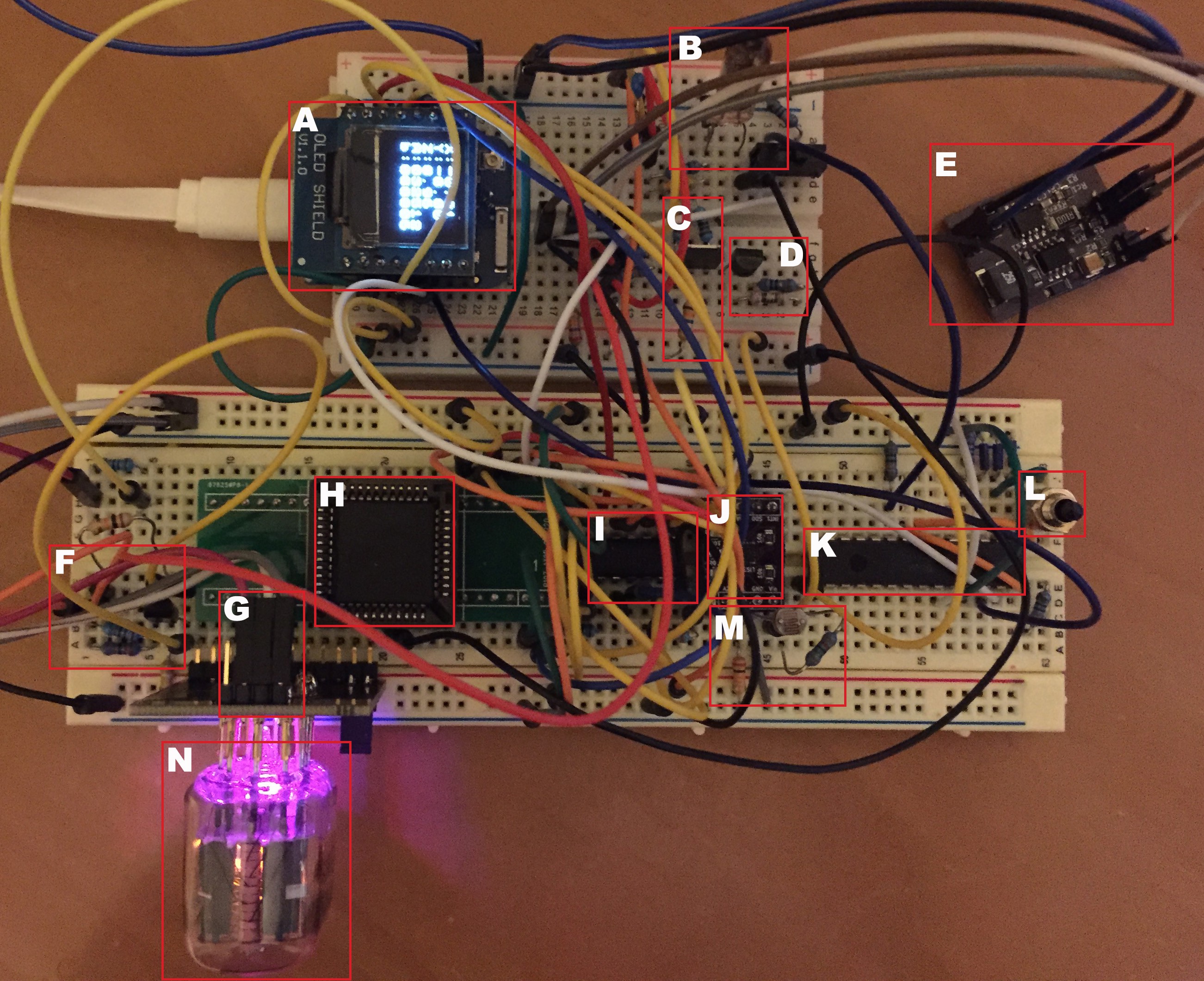
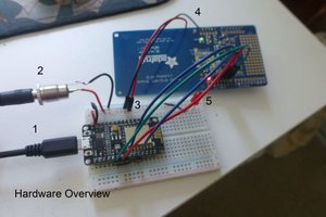
    What you see below is basically that.

    A. Is a Wemos D1 mini pro. It is basically an ESP8266 with all of the GPIOs broken out and it has a USB input. So this satisfies requirements 1, 2 and 8 in one go. What you can actually see is an OLED shield on which I am displaying some debug information.

    B. Is a test colon-separator, an IN-3. I needed to develop the circuitry to drive it.

    C, D and F are different implementations of a constant current source. I could use one of these instead of a current-limiting resistor.

    E. Is one of my HV power supplies that I documented in another project log here on hackaday.io.

    G. Is a connection to a NeoPixel on my adapter board. By using neopixels rather than RGB LEDs, I only have to dedicate one GPIO pin, and I can make each of them do something different if I want.

    H. Is an HV9808. This is a high voltage shift register. It has 32 outputs, so it can drive three nixies plus change. It uses four GPIOs and is easily controlled using the SPI library. This particular chip uses 5V control levels and they can be daisy-chained together so I can control as many nixies as I like, with just the four GPIO pins.

    I. Is a level shifter. The ESP8266 is a 3.3V chip, the HV9808 is a 5V chip. Sigh.

    J. Is an accelerometer. It has an I2C interface, so it takes two GPIO pins, which it shares with any other I2C chips. It also happens to have an analog input, so I connected a light sensitive resistor to it.

    K. Is an IO expander - it adds a bunch more digital out and analog in ports. Is also uses an I2C interface.

    L. Is a test button connected to the IO expander.

    M. Is the light sensitive resistor.

    N. Is an actual nixie tube (an IN-12B) plugged in to one of my adapter boards.

    The aim here was to test that everything I though I might need could actually be made to play nicely together. So far it does. My clock  code does dimming, cross fading, HSV LED cycling, network time synchronization, reads the accelerometer, displays debug on the OLED, reads the button, controls an LED on the IO expander, presents a web page and I can program it over the air.

    One thing noticeable by its absence is an RTC chip. With network time synchronization that automatically adjusts for timezone and DST, why would I need one? The ESP8266 clock is enough to keep time in between synchronizations. Still, I should probably add one just for completeness.

    Here are some videos of it in action. The first is a little blurry, but it shows off the backlighting too. The nixie is a GR10J numicator (swoon):


    This one is of CD-12 and shows the clock display a little better:

    Anyway, we won't need all of this in my one-tube clock, and we'll change up some of the components while we're at it.

View all 9 project logs

Enjoy this project?

Share

Discussions

Jeremy g. wrote 02/07/2018 at 19:15 point

very nice, I thought about using the esp8266 on mine but was space constrained. if you look at my mini clock I have a circuit on there that might interest you. the charging / super cap circuit. also runs off Lipo. 

  Are you sure? yes | no

Paul Andrews wrote 11/16/2017 at 17:55 point

Hi Mike,

The clock uses an ESP8266 (actually it will probably be an ESP8285, but same thing). It won't use the USB to access any data, only for power.

  Are you sure? yes | no

Mike Szczys wrote 11/16/2017 at 16:27 point

Very cool, I'm glad you're taking it to the next level. Should be quite a show piece when done!

Feature request: You mentioned it will run from the USB port and grap NTP from there. It would be cool to see it run from 5V USB power but utilize something like an ESP8266 for the connectivity and NTP pulls. This way you can power it from USB port, or a USB phone charger and it just needs to be on the local network to get updates.

  Are you sure? yes | no

Similar Projects

Does this project spark your interest?

Become a member to follow this project and never miss any updates