-
What's next?
01/12/2015 at 15:34 • 0 commentsThis project gathered a good following, so I'm now wondering where I can bring it next. There are a few things to think about and some decisions to be made. The Teensy conversion should bring very interesting improvements, that could make the product worthwhile for a crowdfunding campaign, and/or make it an interestiong open source project. But this would mean leaving the Nokia part behind, as there are not many 3310 left, the display while good is still quite low res, and there may be copyright problems.
And by the way, I think that the Gabotronics Xminilab and Xprotolab are still the best choice for a device of that kind, even if they're missing the whole current and power measurements that first pushed me to this quest. http://www.gabotronics.com/oscilloscopes/xminilab-portable-oscilloscope.htmI foresee two "extreme" paths, and a whole lot of other viable paths inbetween. The best thing would be a community effort to expand and improve the Xprotolab by porting it to the Teensys Freescale micro (or better) and designing a platform with improved input handling and features; then a plethora of devices could be made, as it happened with the Gongkai ecosystem. I would build a board for the Nokia 3310, someone could build a Fluke lookalike case, or even an oscilloscope in a watch. The easy path would involve just designing boards for the original Xprotolab micro and work with its limitations, maybe with a second micro to handle UI, battery charging etc., as it's already happening with some customer-made Xprotolab devices.
I think that the only innovation that my device brought to the table is the Nokia 3310 "integration", but in the end that's just a gimmick, a novelty. Bringing this project forward would require a great effort, and I don't know if it will be worth it. I've done 80% of the work, with 20% of the effort. Should I leave this here as a nice exercise in creativity and a fun holiday project, or should I try to bring it to the next level by working the other 80% to complete the remaining 20% of the project?
-
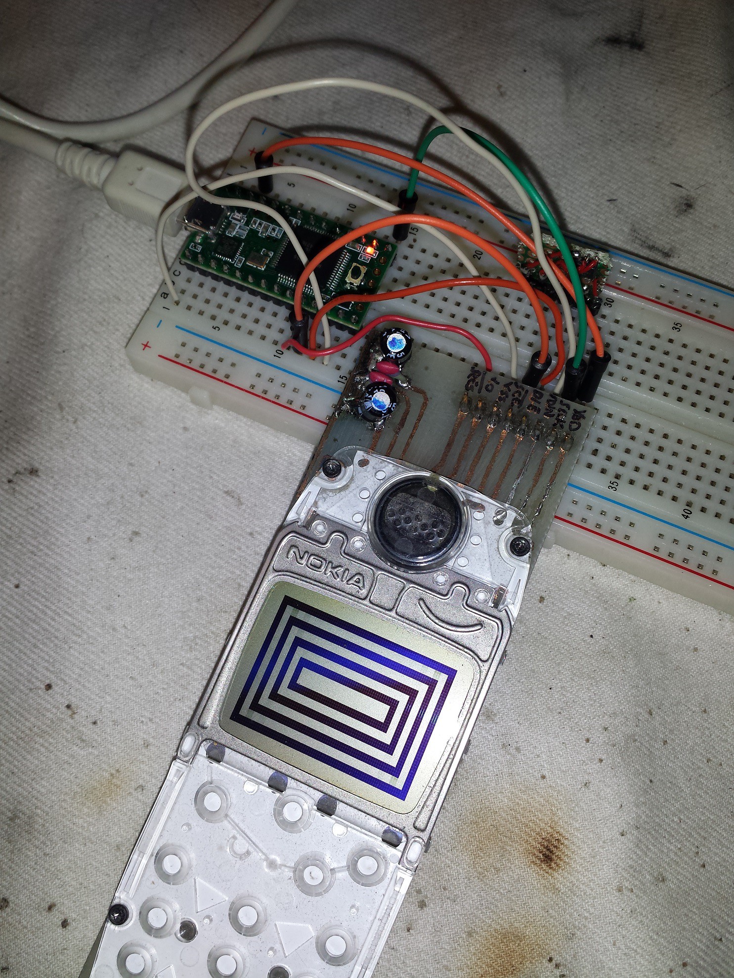
LCD testing with the Teensy
01/06/2015 at 22:04 • 0 comments...and it works! Other than more memory and more power, the Teensy also has two PGAs on board and two separated 16bit A/Ds that should help to improve significantly the original design. Well, the hardest part of the project is already done, now on to the porting!!
![]()
-
ALL HAIL THE 3310 WIZARD!
01/03/2015 at 16:37 • 0 comments![]()
-
Sources online!
01/03/2015 at 15:02 • 0 commentsI just uploaded the sources on my GitHub account! So, do you want to build it? Here's a step-by-step introduction:
- Get all the design files from the main repo: https://github.com/mastrogippo/1337-3310-tool
- Build the hardware!
- Download the firmware, binaries and tools from here: NokiaPack
- If you're lazy go to step 10, if not read on to generate the Font and Bitmap binaries yourself
- Use the PPM editor in the NokiaFirmware folder with the .fls file to export the .pef file with the fonts and a folder with all the bitmaps in the original firmware
- Get the Bitmap converter: https://github.com/mastrogippo/BitmapToBinary
- Place the bitmaps in the "bmp" folder with the BitmapToBinary exe, run the program, select the bitmaps to include and click "Gen"
- Get the PEF Fonts tool: https://github.com/mastrogippo/PEF-Fonts
- Place the font PEF file in the same folder as the PEF Fonts executable, run it to generate the font binaries, save them and the listed offsets
- Get the EEPROM upload tool: https://github.com/mastrogippo/Arduino-EEPROM-Upload
- Upload the sketch to the Arduino (if you have all the hardware conneted, upload the 1337 3310 sketch uncomenting the #define EEWRITE)
- Copy all the bin files to the EEPROM uploader folder and run it (change the serial port in the code if needed)
- Upload the binaries, then click any phone button to end the write process if you're using the 1337 3310 sketch; the phone will beep
- Comment again the #define EEWRITE and upload the sketch
- ???
- PROFIT!!
-
Video recap!
01/02/2015 at 19:38 • 11 commentsAnd here's a video of the latest developments!
-
1337 c0nn3kt0r sk1llz
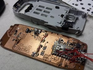
12/26/2014 at 18:09 • 2 commentsWell, today I started testing the analog input circuitry. As you can see, I'm soldering wires directly from resistors to the connector. The casual observer may see this as being too lazy to route a proper connector on the PCB, but it's really a very sophisticated way to relieve stress on the connector! :P
I also had to add a bodge flyback diode to the buzzer, as I forgot to include one... That's the second error on the PCB: the other one is taking for granted that I could put two green LEDs in series. I'm too used to modern, super efficient LEDs, but since I'm reusing the original Nokia 12 years old LEDs, they need a bit more current and seem to have an higher forward voltage than the ones I use everyday. -
PCB design
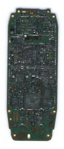
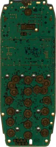
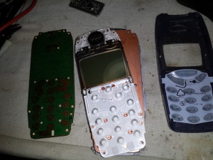
12/26/2014 at 00:53 • 0 commentsDesigning a replacement PCB for the 3310 mainboard requires quite a bit of effort. The first thing I did was to remove all the components from a broken phone, to get a nice scan of the board:
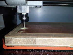
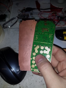
Now I know where all the holes and pads are, and I can draw the outline of the PCB. After a lot of failed attempts and frustration with various open source softwares, I ended up using Adobe Illustrator to create an exportable vector image of the outline and holes to feed to my Roland SRM-20 mill. Here she is cutting the PCB to size:
![20141212_193338]() and here's the result, after a lot of tests on foam to fix minor issues:
and here's the result, after a lot of tests on foam to fix minor issues:![20141212_212104]()
![20141212_214000]() it fit very well, despite the PCB being thicker than the original (1.4mm instead of 1mm).
it fit very well, despite the PCB being thicker than the original (1.4mm instead of 1mm).
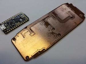
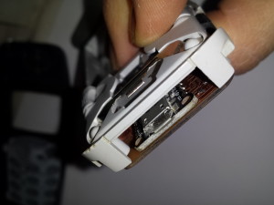
Time to fire up Eagle! I created a library for the phone footprint with the various pads for the LCD, buzzer, battery connector and buzzer and started laying out the board. I wanted to design a board that I could etch at home, so I had to stick with two layers, but I soon discovered that I had to give up the numeric pad to route all traces. I was still able to keep the function buttons, so I guess that I'll live with that for now!
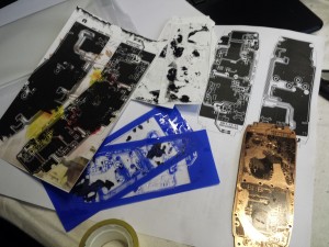
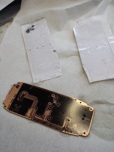
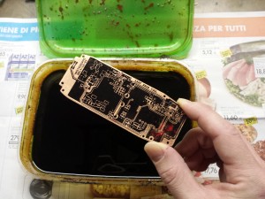
Etching the board was a nightmare by itself, as my printer couldn't print a design this big on wax paper without scratching a lot of the toner away; Press'n'peel is not very good either for big boards with very thin traces. After dozens of failed tests, I was able to transfer the toner well enough with the good old photographic paper technique, being extra careful with every step of the process, even going as far as measuring the temperature of the iron before heating the board.![20141222_141156]()
![20141222_144030]()
![20141222_151055]()
![20141222_161930]()
![20141222_162025]()
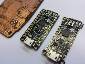
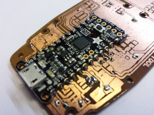
![20141222_162132]() TA-DAAAHHH!! Not perfect, but still very nice and usable. Since the board is sandwitched under the screen plastic frame, I couldn't have anything protruding from the PCB, so I had to transform the Trinket to be surface solderable:
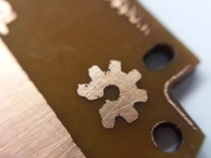
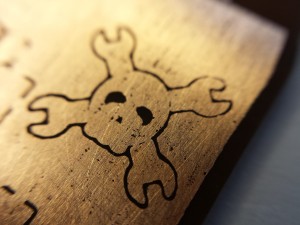
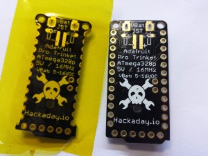
TA-DAAAHHH!! Not perfect, but still very nice and usable. Since the board is sandwitched under the screen plastic frame, I couldn't have anything protruding from the PCB, so I had to transform the Trinket to be surface solderable:![20141222_173530]()
![20141222_173705]()
![20141222_174844]()
![20141222_175430]() Some filing and a bit of kapton to insulate the bottom pads, and I was good to go!
Some filing and a bit of kapton to insulate the bottom pads, and I was good to go! -
Testing the PGA113
12/19/2014 at 15:07 • 0 commentsPGAs are quite common, but I don't have one in my parts bin and I was curious about an idea I had for a while...
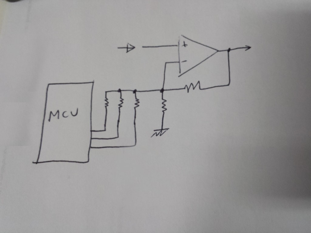
![]() In the non-inverting configuration, the opamp gain is set by the two resistors ratio, and since one of them is grounded, I can add a resistor in parallel by connecting it to the MCU I/O and grounding the pin or setting it as an input to activate or deactivate it.
In the non-inverting configuration, the opamp gain is set by the two resistors ratio, and since one of them is grounded, I can add a resistor in parallel by connecting it to the MCU I/O and grounding the pin or setting it as an input to activate or deactivate it.![]()
I looked around the web but couldn't find anyone supporting/bashing my theory (if someone has links discussing this, please let me know), so I just tried it and it works! With the ATMEGA328P in the Trinket you must connect the resistors to analog pins, or else it will still load the amp too much when set as a digital input. Setting the pin to analog input will leave the resistor floating, and setting it as a low digital output will connect the resistor to ground. This setup is not perfect, especially at low voltages, and it seemed to further reduce the bandwidth at high gains, probably due to the input pin capacity.
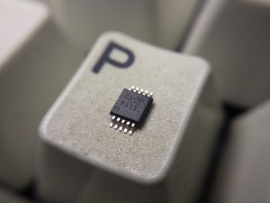
I decided to take the lazy route when designing the input stage, so to get a wide input range while keeping a good resolution I opted for a Programmable Gain Amplifier. I decided to order the Texas Instruments PGA113 as it's cheap, has 2 switchable inputs, a reference pin and a nice range of switchable gains. It comes with a choice of 8 multipliers (1, 2, 5, 10, 20, 50, 100, 200) and while the bandwidth is quite low (230kHz at the highest gain setting), it's still good enough for the Trinket ADC.
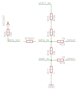
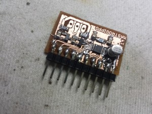
Dividing the input by 1:100 I calculated an acceptable resolution, but to get better results I would really need a 16bit ADC and a lower gains.So here's the input circuitry I came up with:
it should be able to measure both current and voltage at the same time, to calculate instant power consumption.
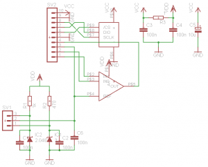
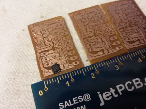
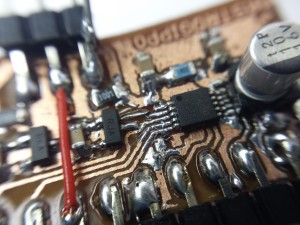
Time to test the PGA!The PGA113 comes in a VSSOP package so I just decided to build a simple breakout board with the basic passives required to make the device work. I also included two precision voltage reference sources, selectable with a jumper.
The board has only one single jumper wire, so it can be printed on a single layer of a dual-layer PCB, keeping the back as a ground plane.
Everything worked on the first try! The PGA113 is quite simple to work with, and the datasheet is clear and complete; it was just a simple matter of modifying the SPI/digitalPot example to send the right two bytes, and I had my PGA working!
// include the SPI library:
#include <SPI.h>

#define PGA_CS 10

void setup()
{
pinMode (PGA_CS, OUTPUT);
SPI.begin();

SetPGA(0,0);
}

void loop()
{
}

void SetPGA(int G, int Ch) {
 //take the SS pin low to select the chip:
 digitalWrite(PGA_CS, LOW);
 //send in the address and value via SPI:
 SPI.transfer(0x2A);
 SPI.transfer((G<<4) + Ch);
 //take the SS pin high to de-select the chip:
 digitalWrite(PGA_CS, HIGH);
}
That's it! Now on to the 3310 PCB design!
-
Nokia firmware reverse engineering
12/04/2014 at 21:10 • 0 commentsA long time ago, (I felt like) I was the coolest kid on the block, with my heavily modified Nokia 3310. A thriving community existed with the purpose of reverse engineering Nokia DCT3 phone firmwares, creating from the simplest mods like changing a few bitmaps to writing a full alternative open source firmware, aka Project MADos. Yes, I was “cooking ROMs" before it was cool.
This is what I'm talking about:
As the years passed, everyone got new phones and these projects got abandoned. While I was writing this article and working on my project, I looked back at the iconic websites of that era to find myself in a ghost city full of dilapidated buildings. blacksphere.tk is now just a black page. nokiafree.org attempted to renew itself providing recent Nokia news, but got abandoned early this year (but still kept the awesome forum archive). g3gg0.de, the website of one of the legendary hackers that put a lot of effort on the reverse engineering, lost a lot of the old content in an update and stopped updating his blog in 2013. Most of the links point to dead websites, and it's getting harder to find copies of the tools and firmware images. I'll upload some later.
A 3310 phone has a very simple memory mapping:0×200000 – 0×340000 firmware
0×340000 – 0x3D0000 PPM
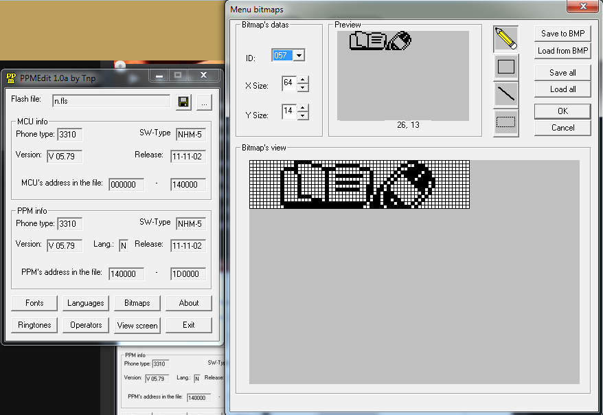
0x3D0000 – 0×400000 EEPROMand the PPM is what I'm looking for: it stores all the localization data (strings and operator list), fonts, ringtones and bimaps. PPMEdit is a nice piece of software to edit and export that data.
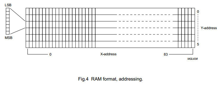
![]() On the Bitmaps window, you can find and edit all the images and export them as single .bmp files. So I just have to convert them to store the data on an external eeprom because the Trinket board that I'm using doesn't provide enough memory to store all that stuff. The PCD8544 display stores the data in this order:
On the Bitmaps window, you can find and edit all the images and export them as single .bmp files. So I just have to convert them to store the data on an external eeprom because the Trinket board that I'm using doesn't provide enough memory to store all that stuff. The PCD8544 display stores the data in this order:
so I'll just pre-align the data in a way that will not require any further processing by the MCU, that will just have to read and forward it. I played a while to see if I could directly connect the SPI MOSI from the eeprom to the MISO of the display, to save buffering and time during transfer, but this would increase complexity a lot if I wanted to access the display from the MCU too so I'll leave this exercise for another time.![]()
You can find the C# code I wrote to handle this conversion in my github: https://github.com/mastrogippo/BitmapToBinary
![]() Preparing the fonts is a bit harder, as they are exported with a custom file format. It's not complicated at all, and I'm working on a tool to prepare that data for easy access too, but that's not quite ready yet. As the display memory is arranged in six 8bit-high rows, it's very easy to use the small fonts. Putting fonts between the rows or using the large/bold one (13px high) will require a lot of effort and CPU power, so I won't implment it now. Ladyada's library does it and eats up 35% of the flash available, and I can't afford it right now! :)
Preparing the fonts is a bit harder, as they are exported with a custom file format. It's not complicated at all, and I'm working on a tool to prepare that data for easy access too, but that's not quite ready yet. As the display memory is arranged in six 8bit-high rows, it's very easy to use the small fonts. Putting fonts between the rows or using the large/bold one (13px high) will require a lot of effort and CPU power, so I won't implment it now. Ladyada's library does it and eats up 35% of the flash available, and I can't afford it right now! :) -
LCD and external storage working!
11/28/2014 at 18:53 • 0 commentsToday I got the LCD and an external FRAM working. I usually don't care much about aesthetics, but big part of this project is the Nokia 3310 styiling, so I'm taking extra care to emulate the phone as much as possible!
I had some FRAM samples, so i opted for the FM25V10. With 1Mbit of memory, it can store 260 full screen images for the 84*48 LCD. Without huge optimizations, I can load and display an image in about 7ms.
 Mastro Gippo

 In the non-inverting configuration, the opamp gain is set by the two resistors ratio, and since one of them is grounded, I can add a resistor in parallel by connecting it to the MCU I/O and grounding the pin or setting it as an input to activate or deactivate it.
 On the Bitmaps window, you can find and edit all the images and export them as single .bmp files. So I just have to convert them to store the data on an external eeprom because the Trinket board that I'm using doesn't provide enough memory to store all that stuff. The PCD8544 display stores the data in this order:
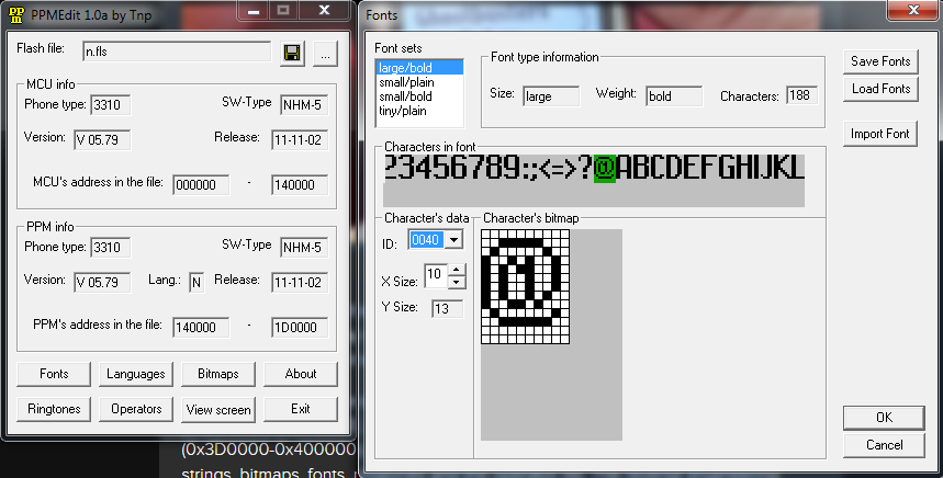 Preparing the fonts is a bit harder, as they are exported with a custom file format. It's not complicated at all, and I'm working on a tool to prepare that data for easy access too, but that's not quite ready yet. As the display memory is arranged in six 8bit-high rows, it's very easy to use the small fonts. Putting fonts between the rows or using the large/bold one (13px high) will require a lot of effort and CPU power, so I won't implment it now. Ladyada's library does it and eats up 35% of the flash available, and I can't afford it right now! :)