 Hacker404
Latest Updates:
Sunday 24 April -
Project log added.
Details:
This is just an 'idea' of the parts and I am sure things will change.
- Z80 CPU, probably NMOS
- ROM - probably FLASH, perhaps large so as to use as FDD replacement.
- RAM - Just SRAM too easy, but still with RAS CAS on expansion connector.
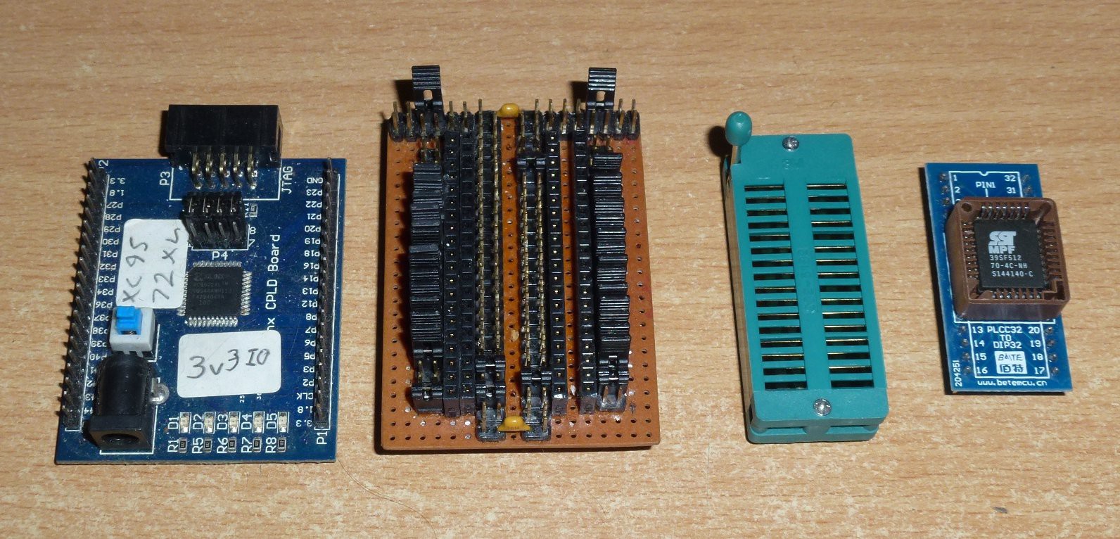
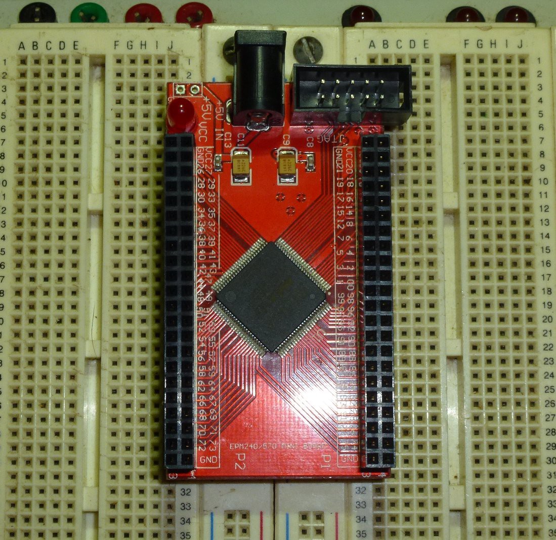
- CPLD - Glue logic / video. Xilinx XC9572XL (easy to solder) or Altera EPM750 (cheaper to program).
- OP-Amp - for cassette port filtering.
- 7805 V Reg - and we're done! (The rest is connectors).
Some thoughts -
The Video is not standard but close enough to NTSC to work, also needs a PAL variant - set with jumper.
Two approaches:
- 100% hardware compatibility, hard to do and many extra parts like character ROM, more expensive.
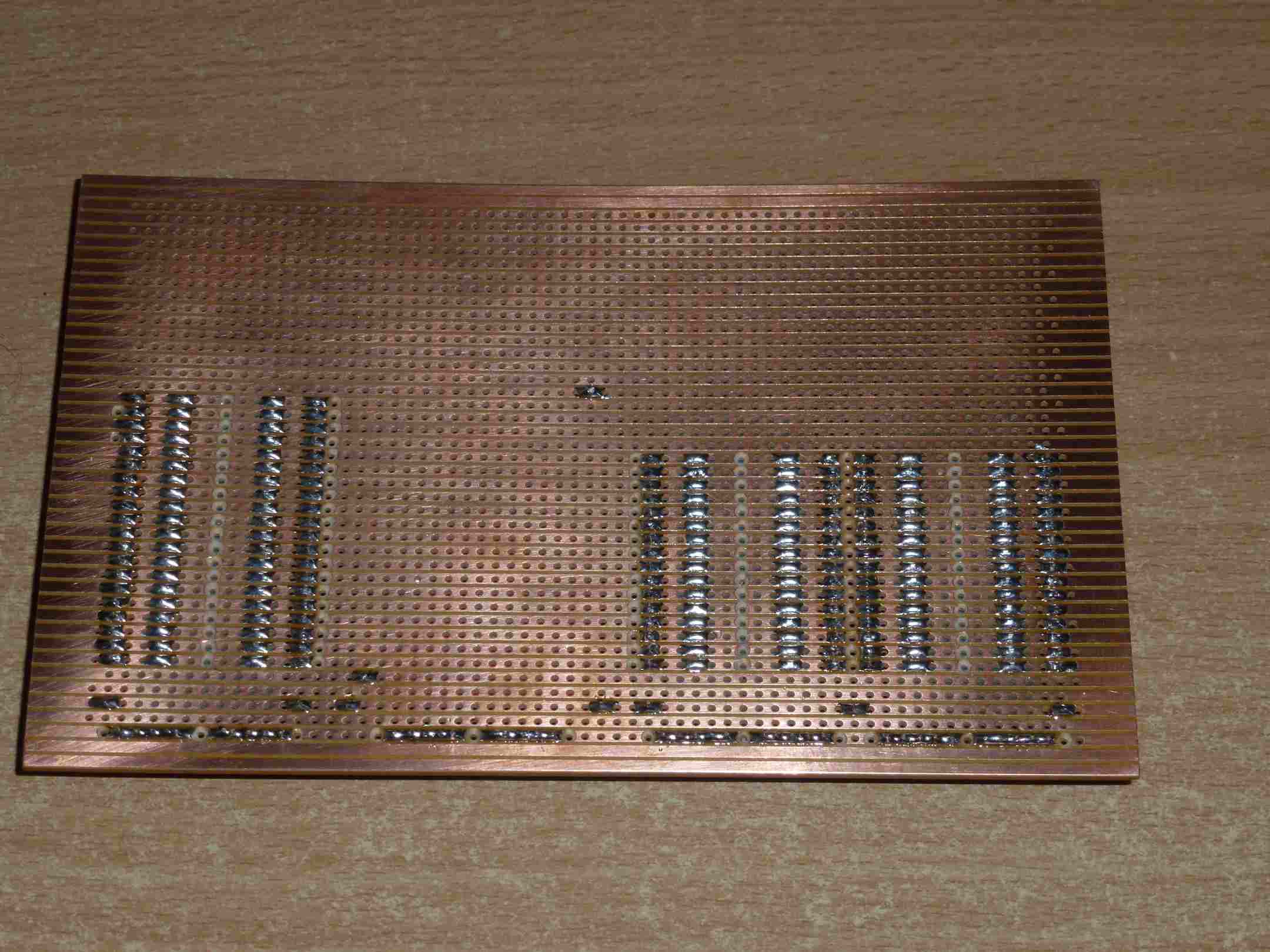
- Hardware compatible on expansion Bus (and I/O) connectors only. Saves some corners like only one FLASH for ROM (no separate Char ROM) and only one (S)RAM chip, saves PCB board space which is cheaper to make by time division multiplexing of the system bus at a higher rate than CPU access. Would also get rid of screen flicker (mostly).
NOTES:
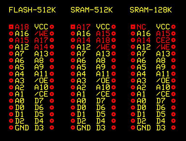
SRAM available in 32kB, 128kB, 256kB or 512kB in DIP packages.
Perhaps the 128kB chip as it is still cheaper than a combination of two chips.
FLASH available in 128kB and 512kB in DIP packages.
Perhaps the 512kB FLASH as it's still a 32Pin and may serve as a emulated FDD. Who knows ...
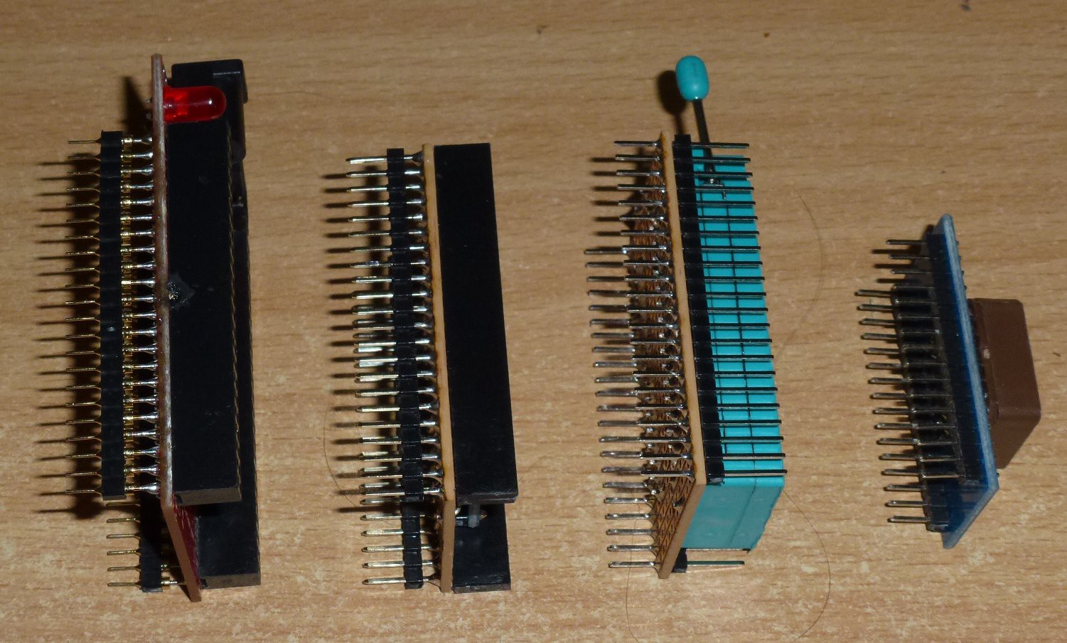
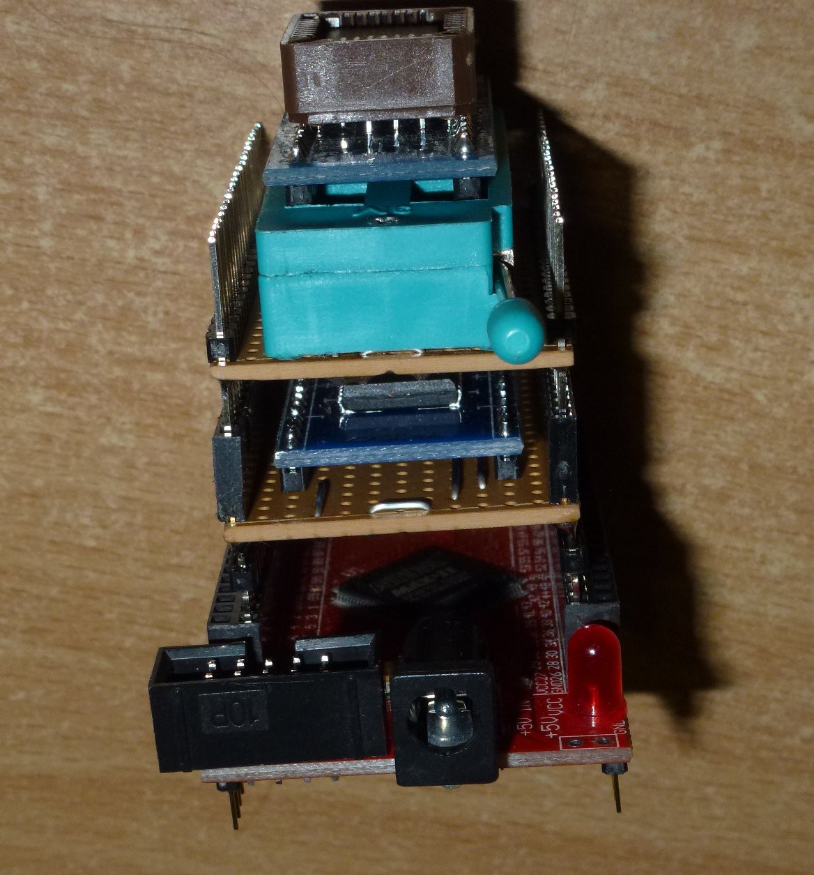
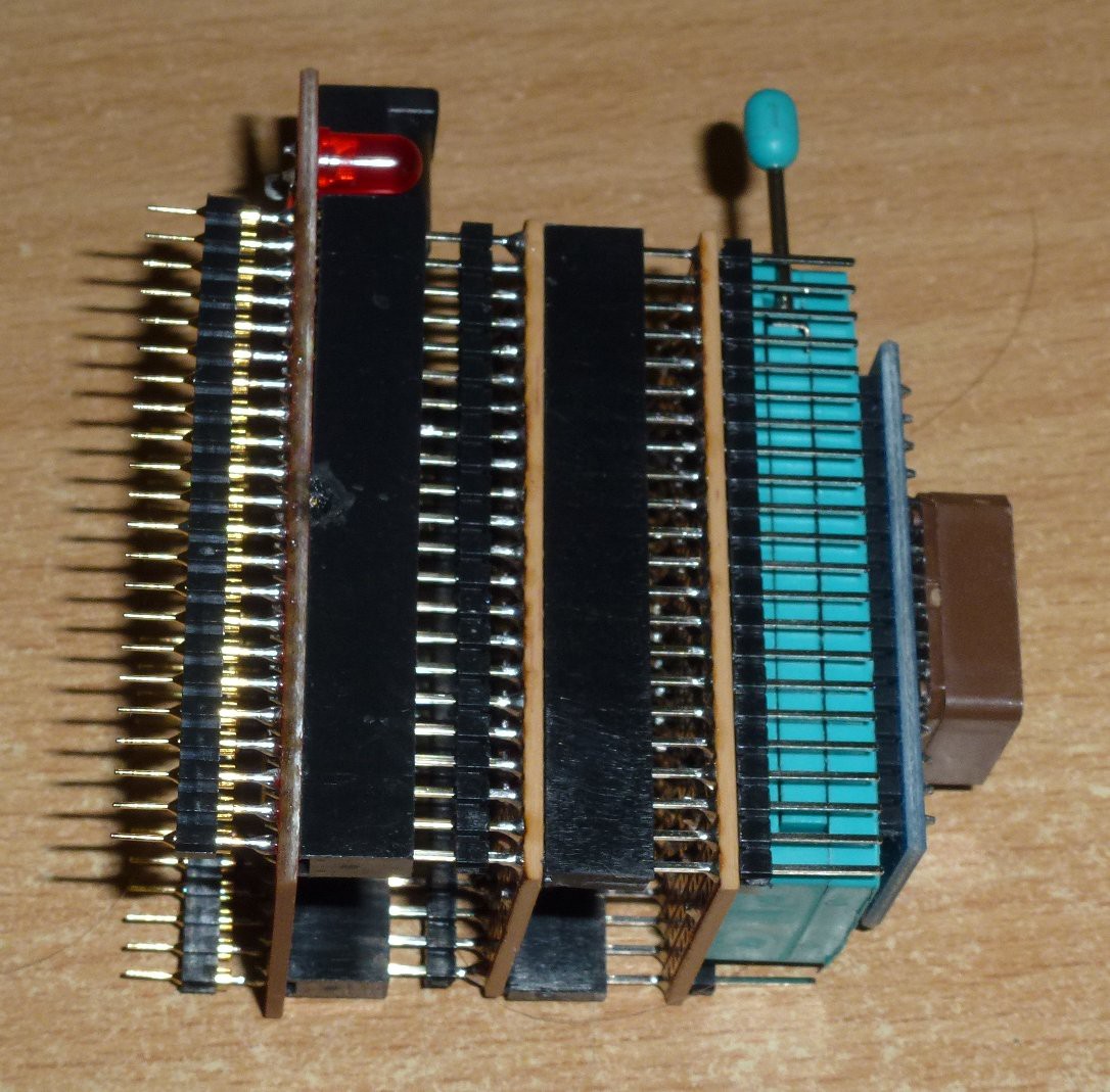
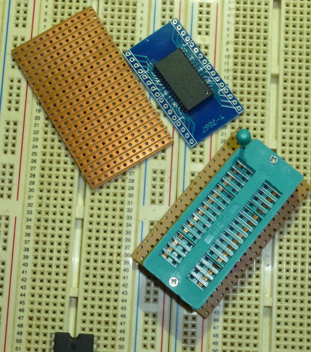
I can't get any of the above here in my country so I will have to work with adaptors.
I don't have any clue as to where I can get such a weird crystal (10.6445MHz). The dot clock seems to come from this (will confirm) also divided by 6 for CPU clock.
So I am thinking of going with:
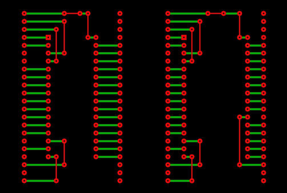
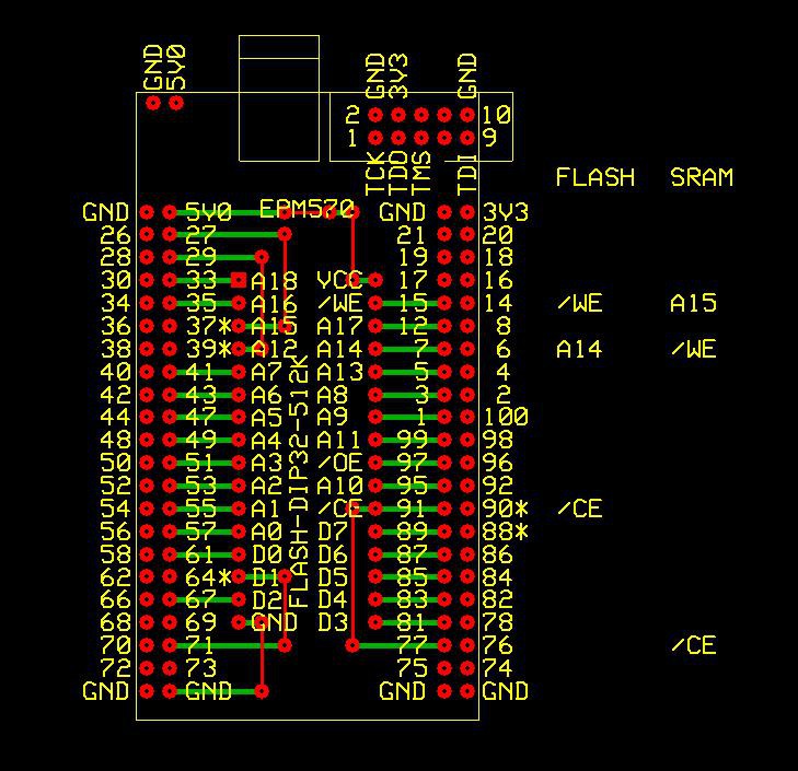
32 Pin DIP socket for FLASH and SRAM anything from 64kB to 512kB will fit in the socket if you can find it - probably 128kB SRAM and 512kB or 64kB FLASH.
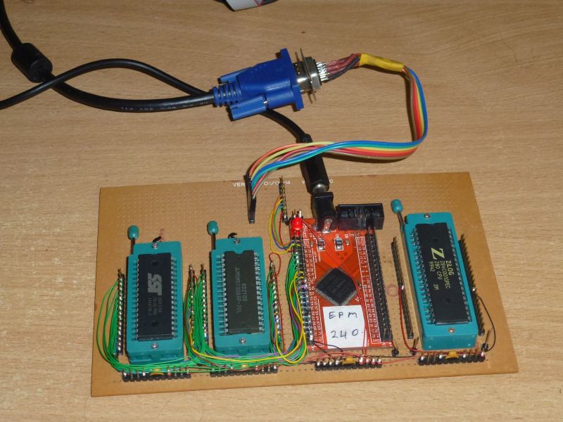
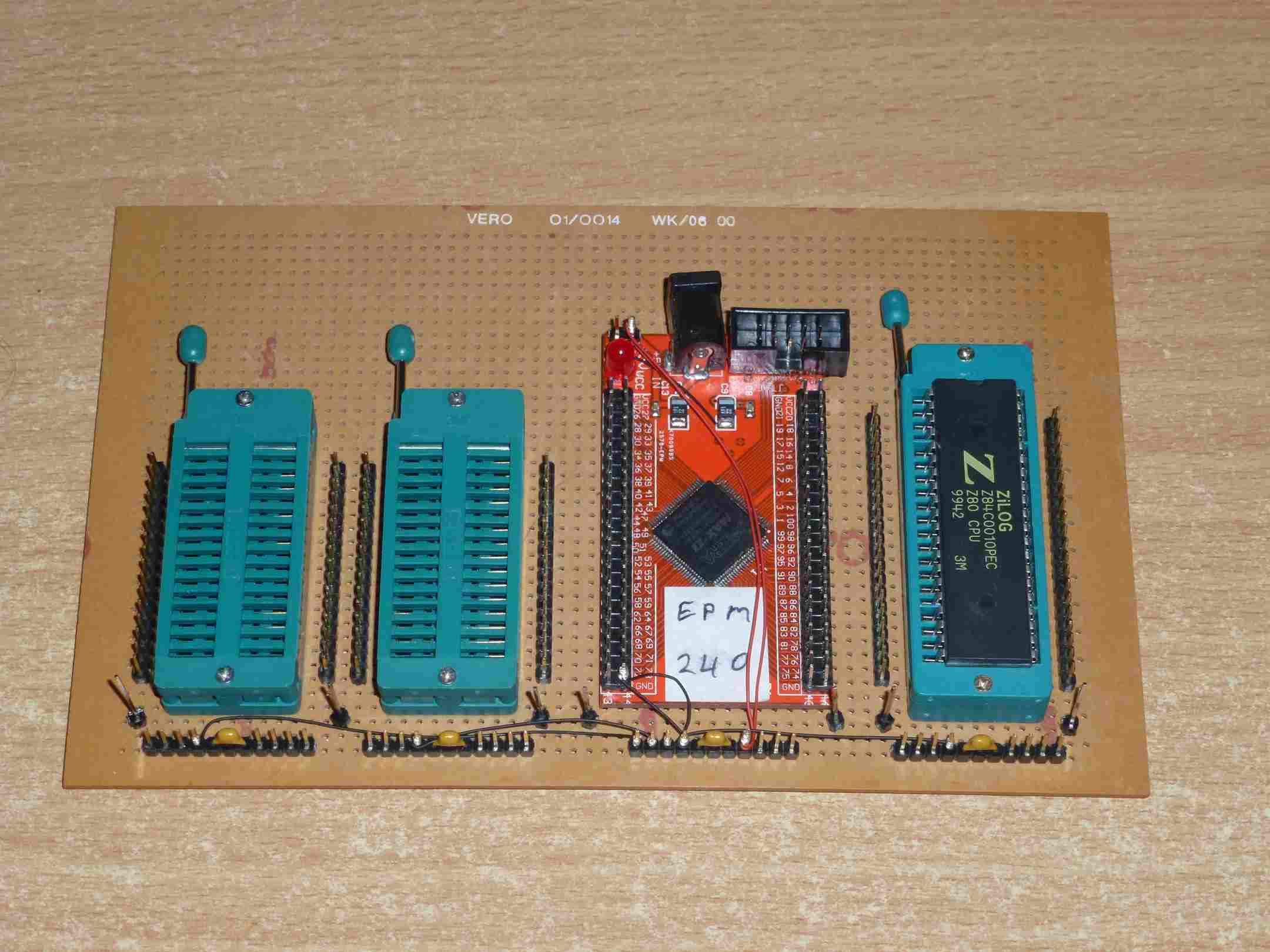
40 Pin DIP socket for the CPU. The NMOS 10MHz version is still available in DIP.
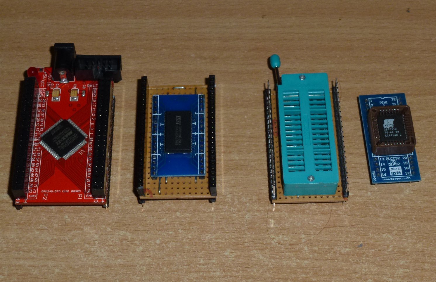
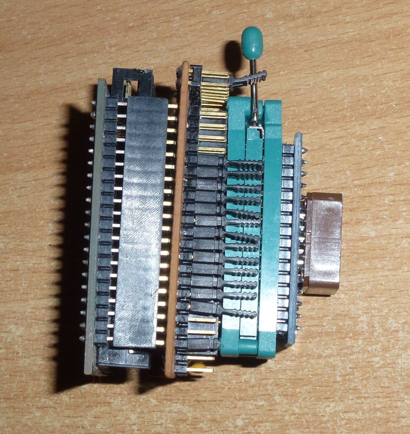
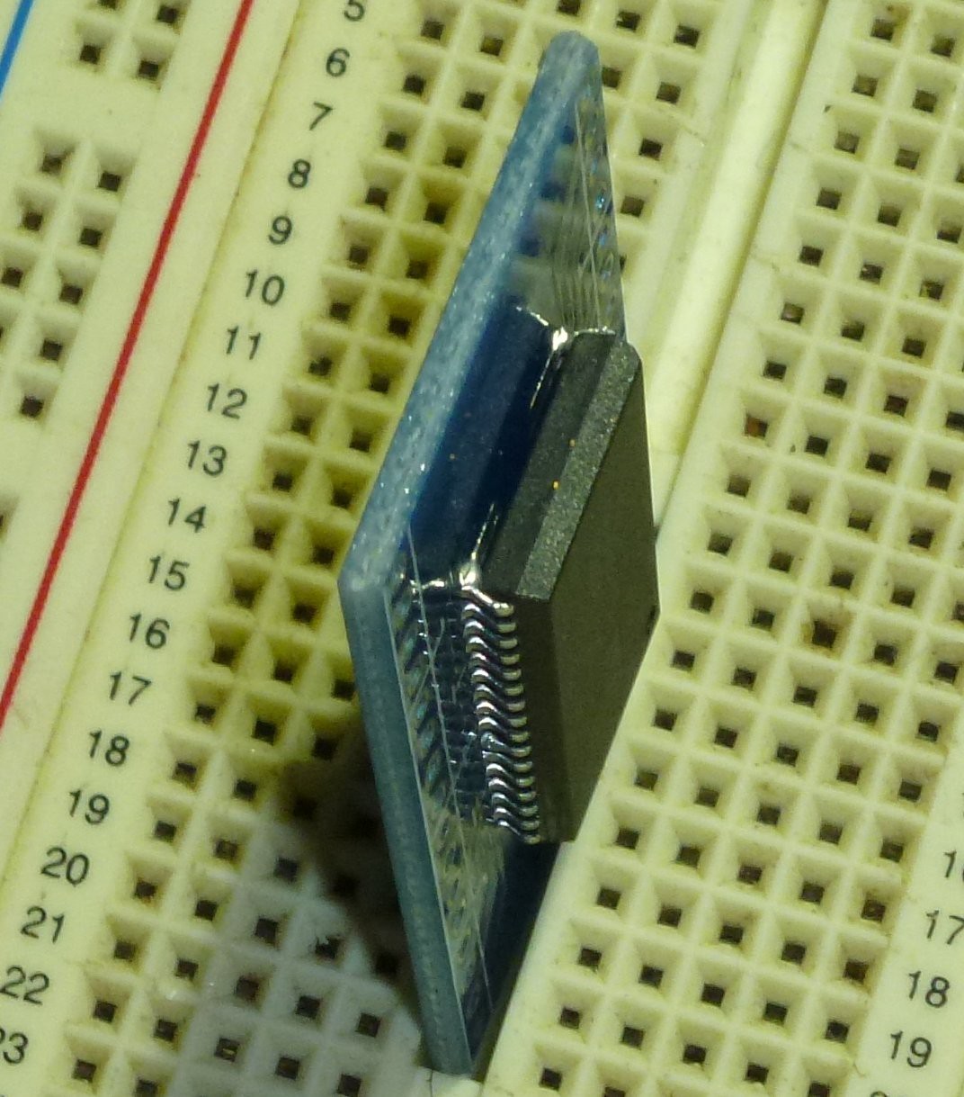
44 Pin DIP for the CPLD. The actual chip is QFP44 Pin so it will sit in a 'standard' QFP to DIP adaptor and have a funky pinout.
Next Steps:
Do a pin count on the expansion bus to see if a 44 Pin CPLD will cut it. If 'YES' then design prototype PCB or (god forbid) try to bread board it.
If 'NO' then try to work out how I am going to mix 0.1" spacing, single sided PCB and a QFP100 chip in the same space.
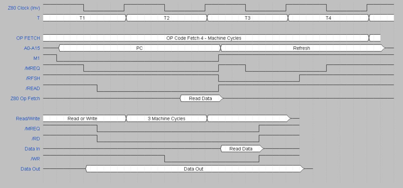
(NOTE: The NMOS and CMOS versions handle OUT(port), register differently, one puts 0xFF on the upper Address bus and the other puts 0x00 on same. Will this effect operation ?) ie are the ports mapped to an 8 bit address space or a 16 bit address space.
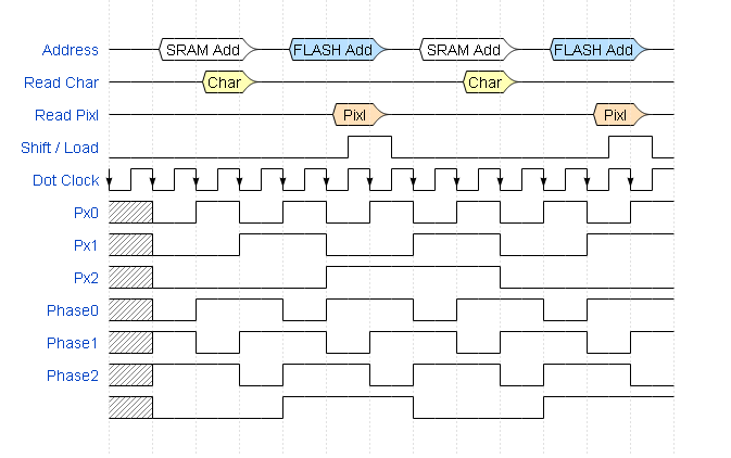
Video and Graphics:
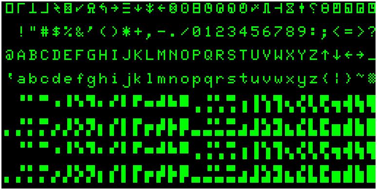
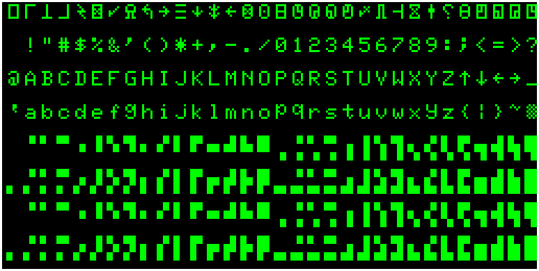
The screen is 63x16 Char cells or 128x48 Graphic cells.
One Char is 7x5px in a 12x6px cell
One Graphic is 3x4px in a 12x6px cell
Total resolution is 384px by 192px, that is 2 horizontal px to every vertical px and has to be converted to an aspect ration from 2:1 to 4:3
For VGA the closest matches are:-
800x600 :- 384x2 => 768 (of 800), 192x3 => 576 (of 600)
Clock frequencies for the above VGA format are 40MHz (60Hz refresh, 628 Lines/Frame) and 50MHz (72Hz refresh, 666 Lines/Frame)
768x576 :- 384x2 => 768 (of 768), 192x3 => 576 (of 576)
Clock frequency for the above VGA format is 34.96MHz (60Hz refresh, 592 Lines/Frame)
NTSC is 525 Lines/Frame??? Anyone help? I have PAL here.
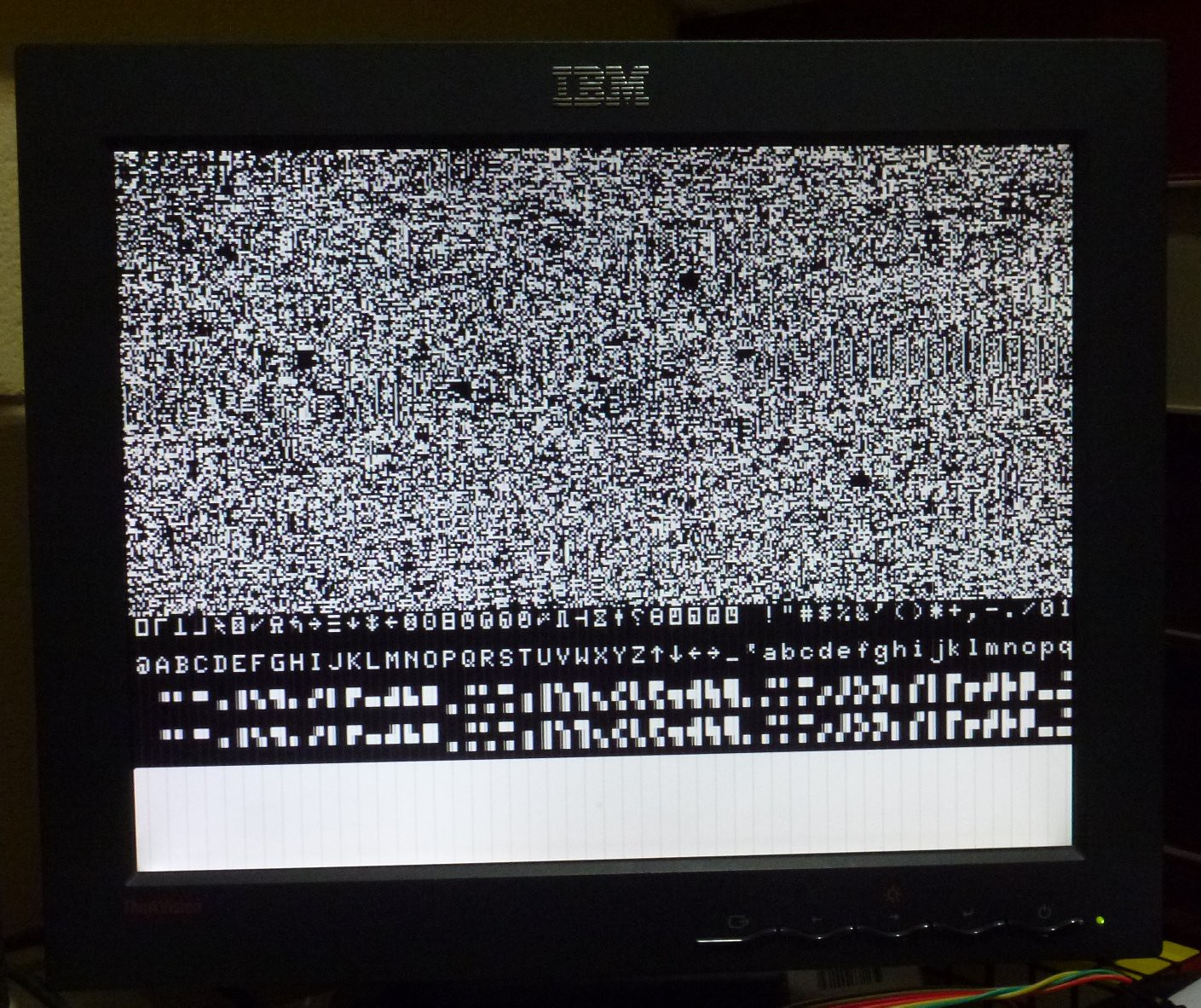
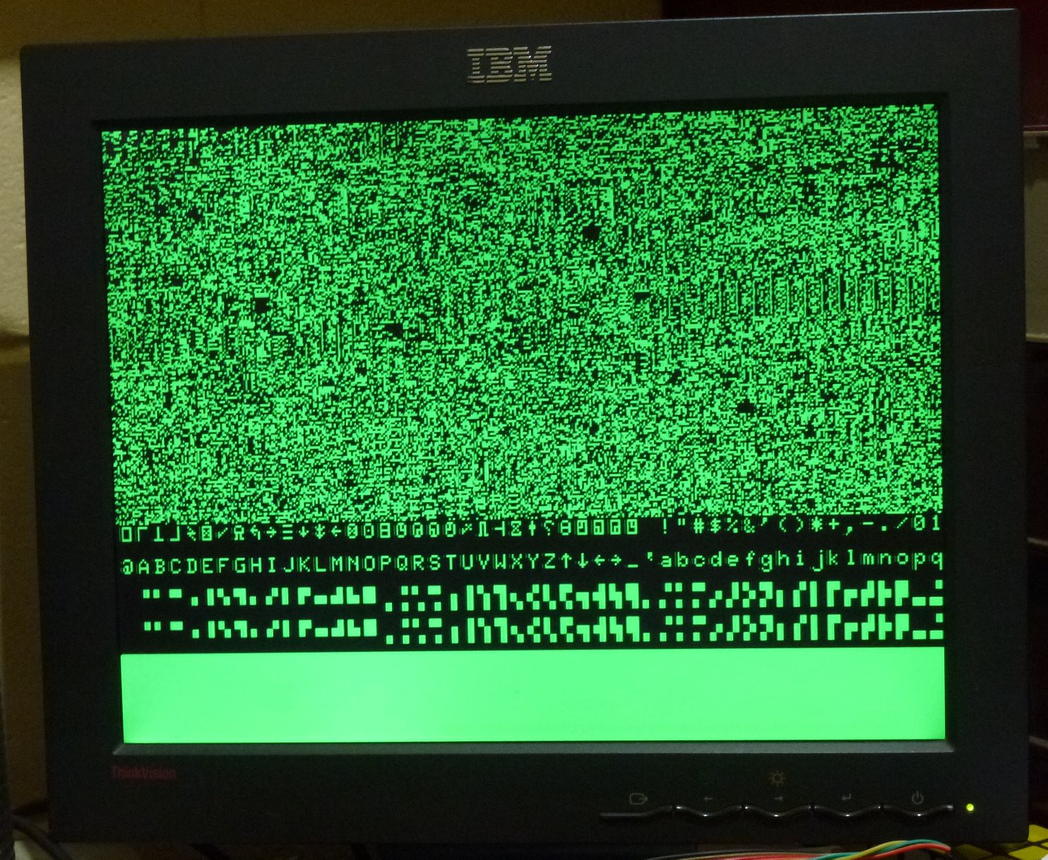
It looks like there are four desired standards: NTSC Composite, PAL Composite and VGA and the original. (I can't fit all four into the smaller CPLD).
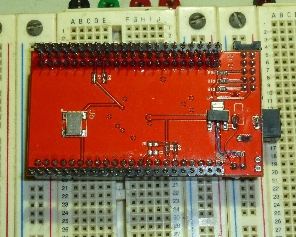
I am going to proto with 50 MHz first because the development board has a 50 MHz oscillator. This means the closest match for CPU clock is 50 / 28 MHz or 1.7857 MHz.


Judging from how old the last post on this page is, it could be that this project has died... however...
I was reading about the problem you encountered with the video needing access to the RAM (and ROM) at the same time as the CPU. Not a problem on the real hardware as they were separate because the RAM chips were so small. A solution used long past for such problems was dual ported RAM, but I don't know if that is still a thing.
An alternate approach might be to "dual port" standard RAM by running it at double speed big problem back then, not a problem now). First cycle is access by the CPU, second cycle is access by video generator, repeat. All handled through the CPLD/FPGA (it may just need to handle chip selects and not the full A & D bus). I really think you should upgrade the chip to the 100qfp though, you said already that the 44 pinner was too small for what you had and there was no room for tape IO etc. You don't want to go budget on such a cool design!
Great project. I'd like to see it live.