-
Prototype #5
05/28/2015 at 07:26 • 0 comments![]()
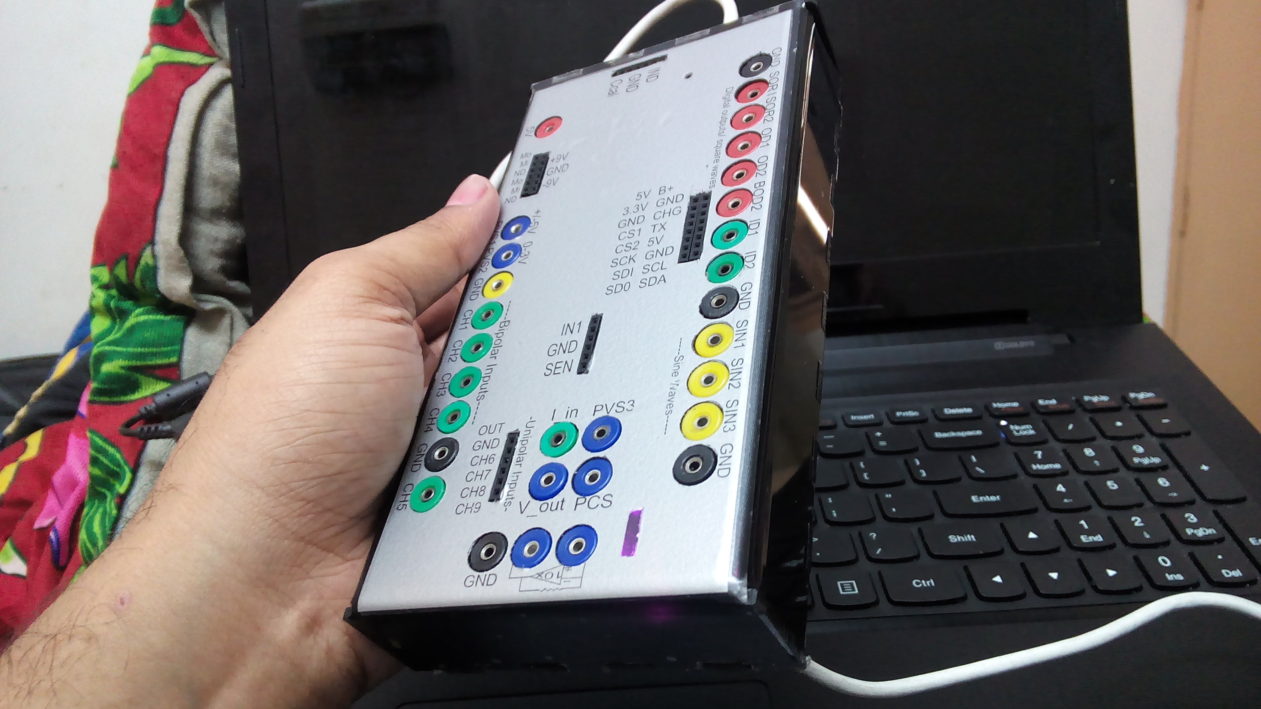
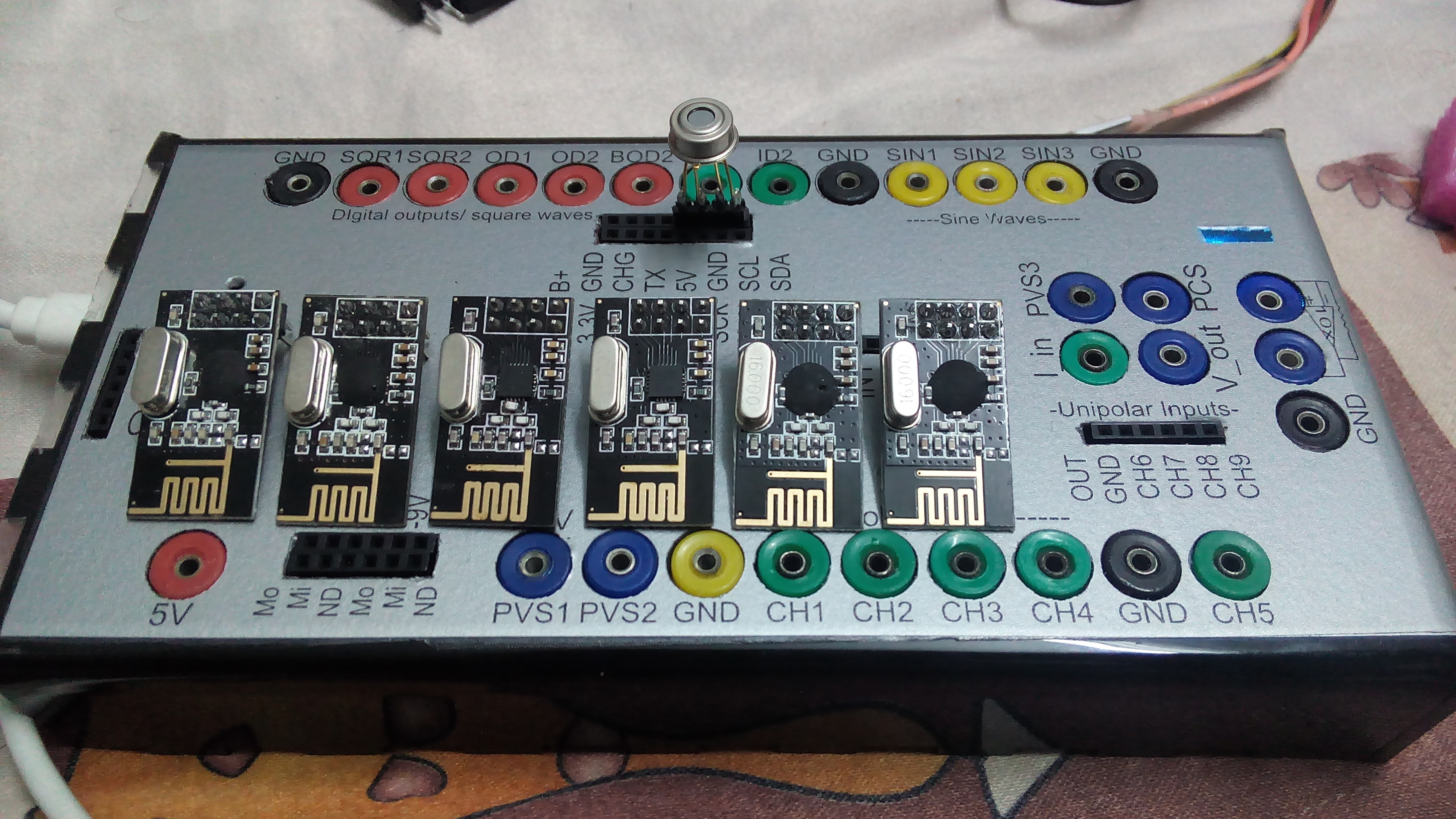
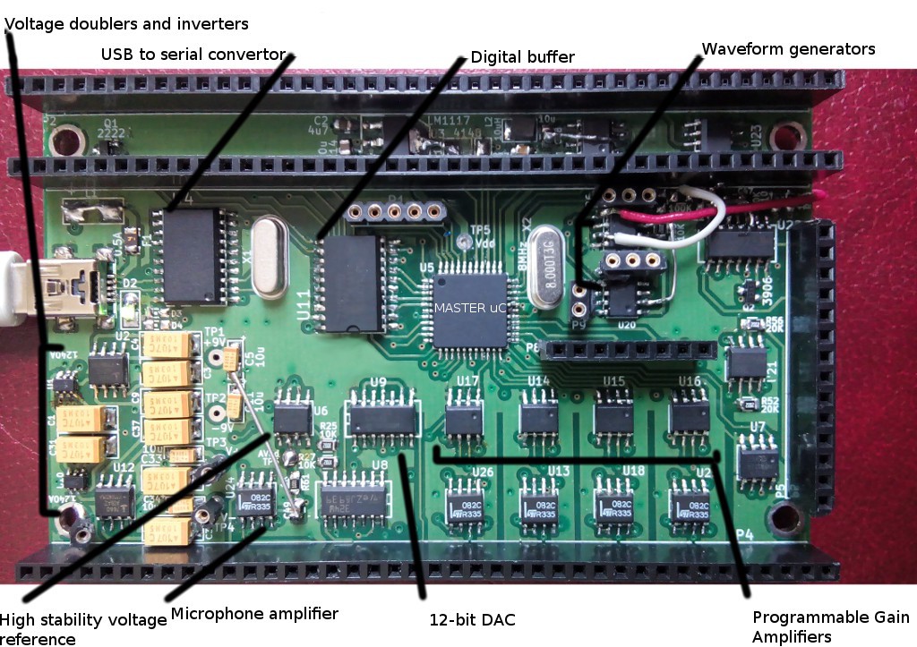
Moved to a larger form factor.
Replaced several crucial input connectors with banana sockets that are more reliable.
These include:
- CH1-CH5 - Oscilloscope inputs + 1 high impedance input
- ID1,ID2
- SQR1,SQR2,OD1,OD2
- I-V convertor
- Sine Wave generators
- PVS1 , PVS2, PVS3
- 5V, GND
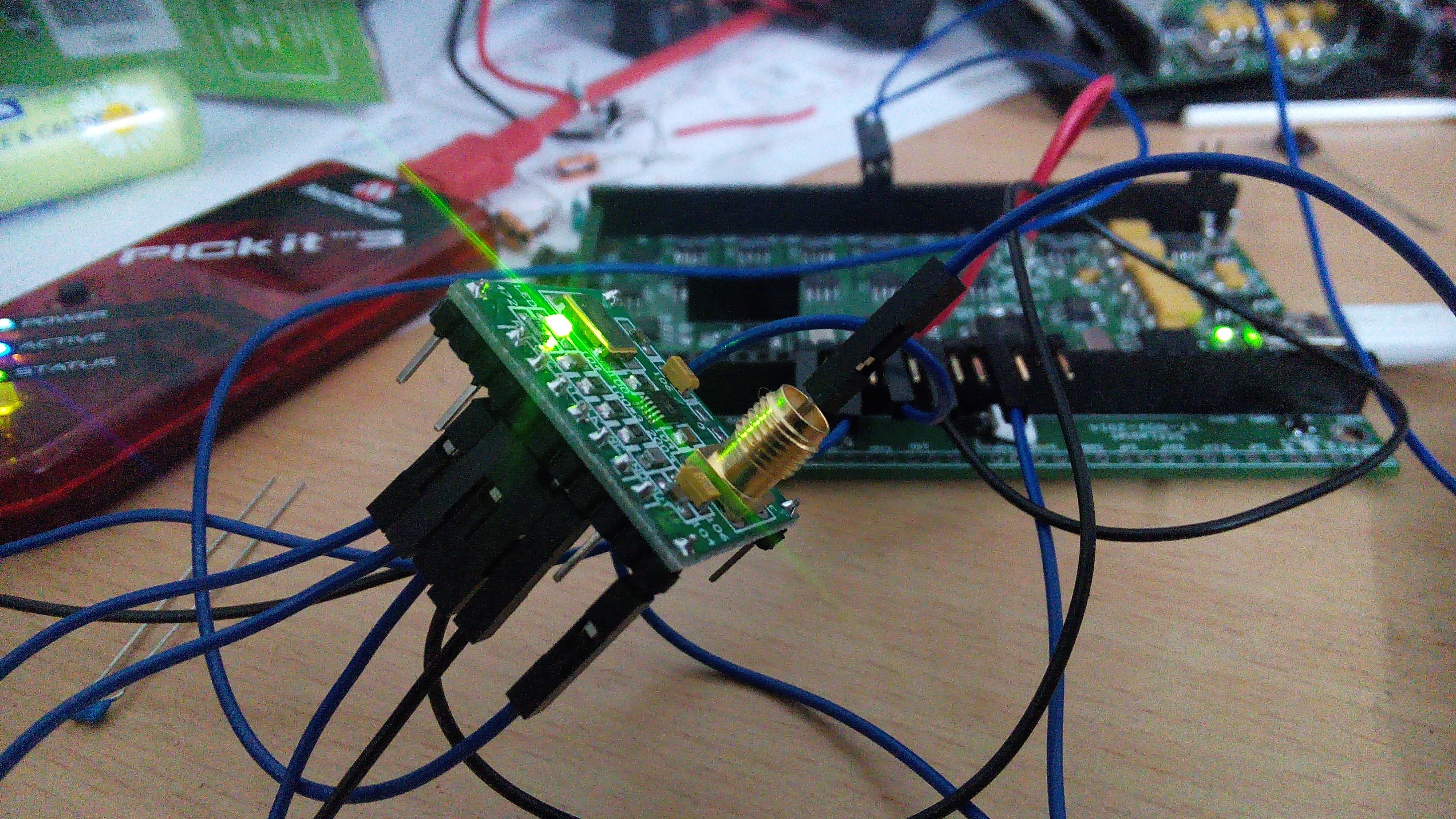
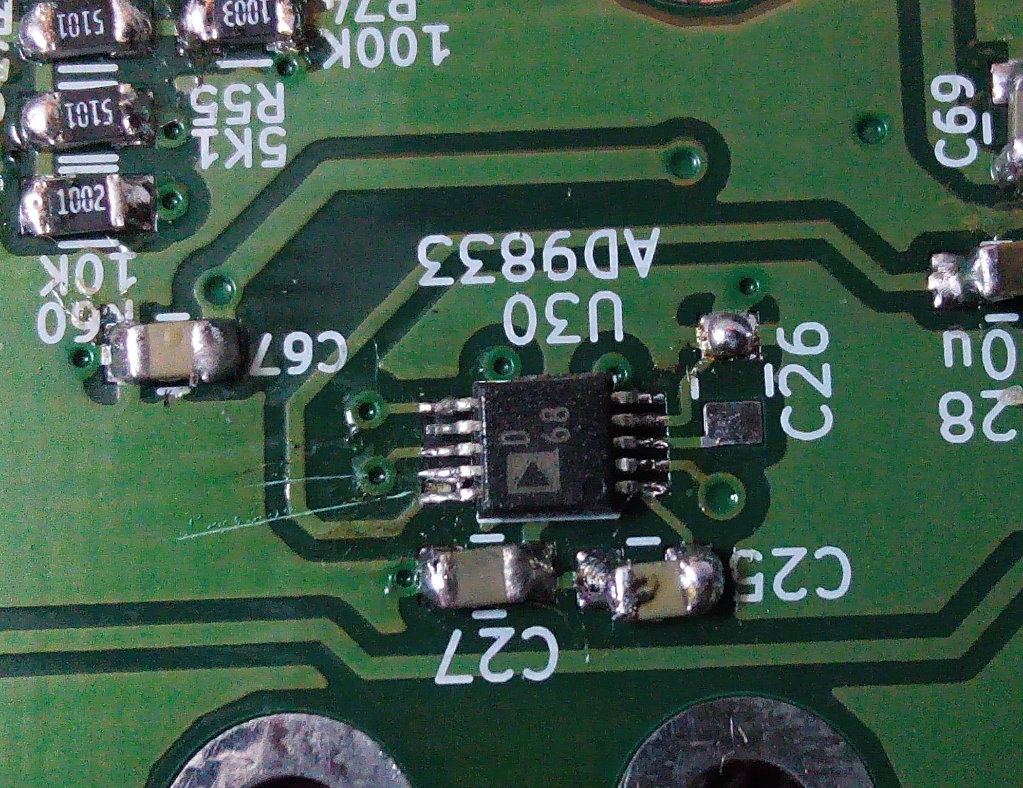
Included an AD9833 28-bit DDS in addition to the two phase correlated PIC1752 based wavegens.
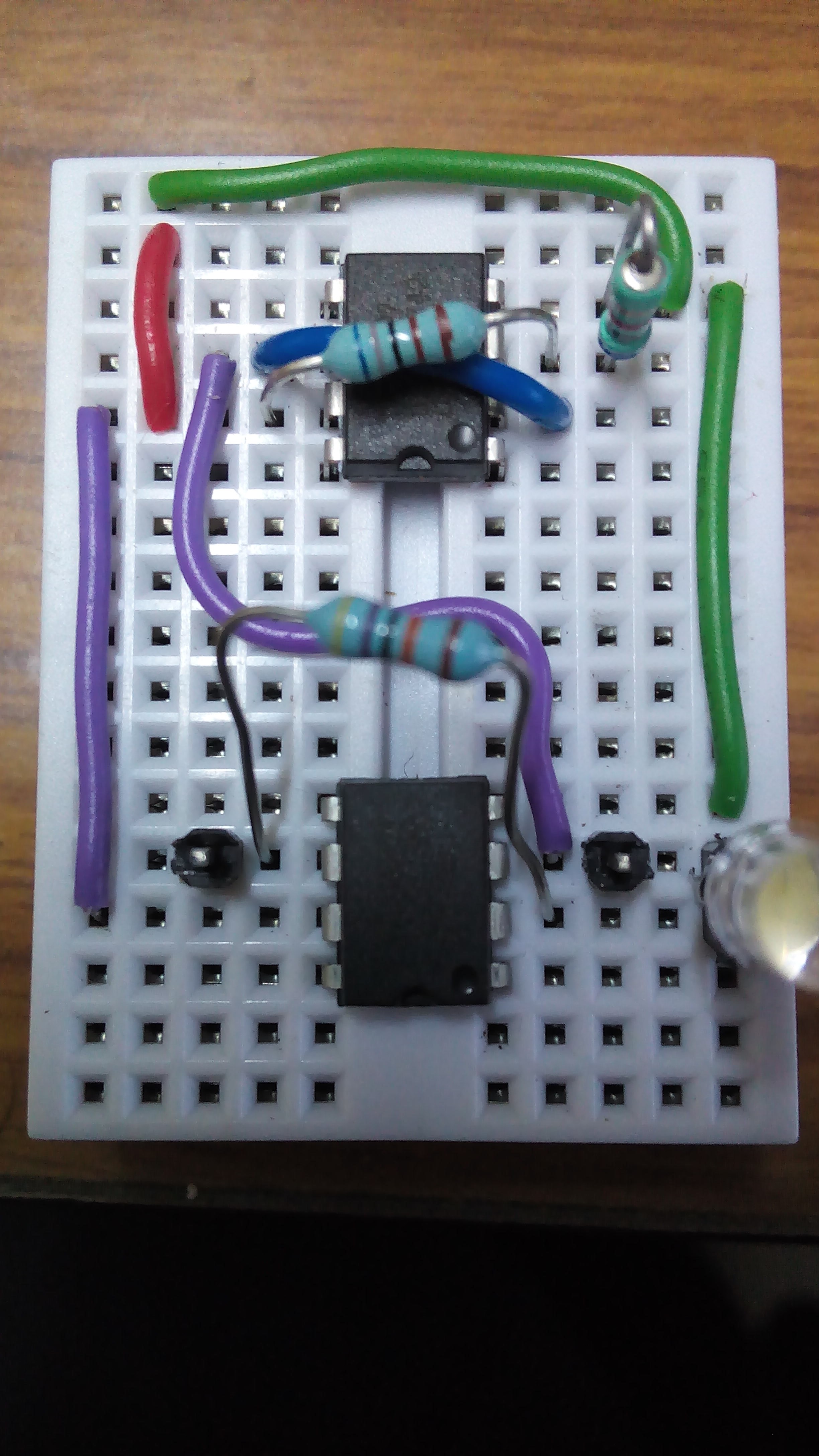
This is the module I used for testing the AD9833 before including it on the main PCB
![]()
![]()
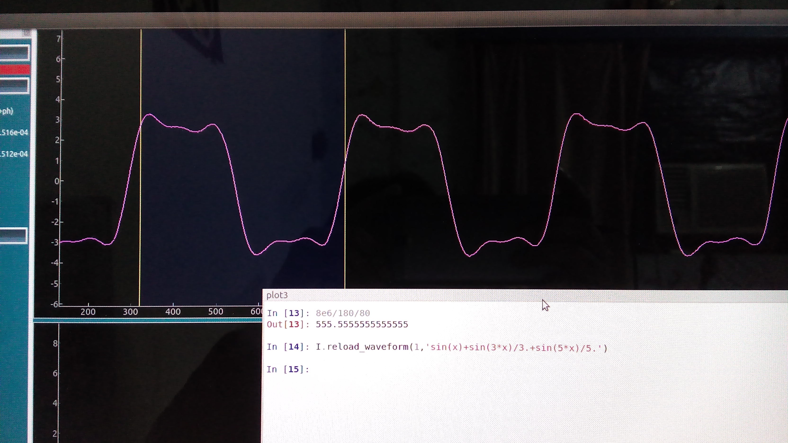
Since The PIC based wavegens use a a table I programmed, I added the ability to edit those tables in order to enable arbitrary waveforms. Subject to frequency response limitations.
The image below shows how easy it is to load arbitrary waveforms. Python accepts your function( In this case it;s the first three terms used to construct a square wave from sines ), and generates the corresponding table before loading it onto the PIC wavegen.
Sadly, the more powerful AD9833 is limited to sine, triangle and square waves.
![]()
NRF radios arrived. Looking forward to making wireless modules.
![]()
Visited several Laser cutting faciities to try out different enclosures for the prototype boards.
Will add a separate log for those
-
Bandpass filter characterization
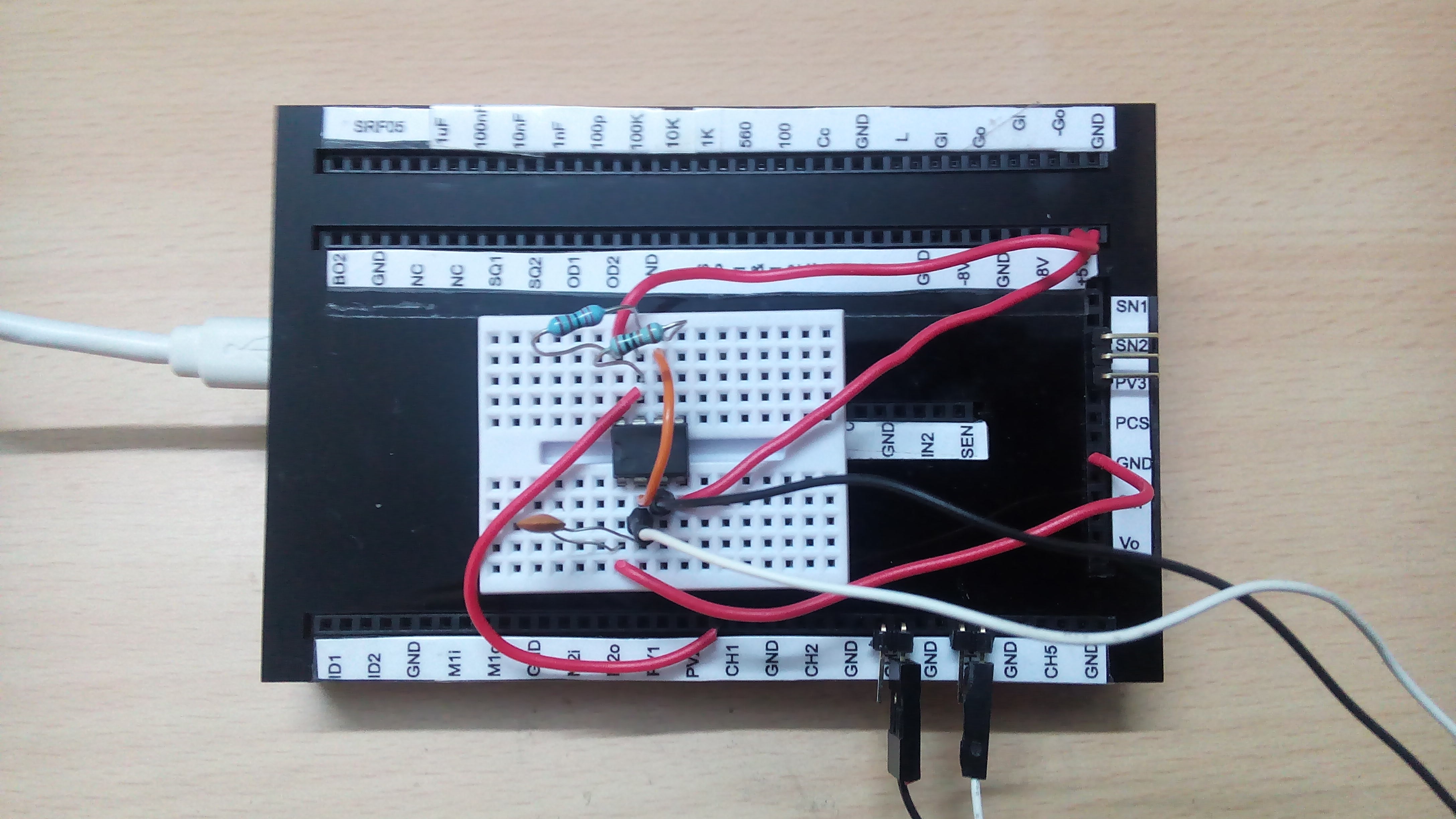
05/27/2015 at 10:40 • 0 commentsThe PIC12F1572 based sine wave generator was used to sweep the input signal frequency of an active bandpass filter I made. Both the input and output were monitored using the device's oscilloscope. Scipy was used to fit the waveforms to a sine function and extract parameters.
Extracted Amplitude and phase were plotted against input frequency.
![]()
This is the only picture I have. I made the connections properly, but later.
The PIC based waveform generators were later replaced with AD9833 DDS chips which offered 28-bit frequency resolution, and 12-bit phase control in addition to other features such as FSK capability
-
Prototype #4
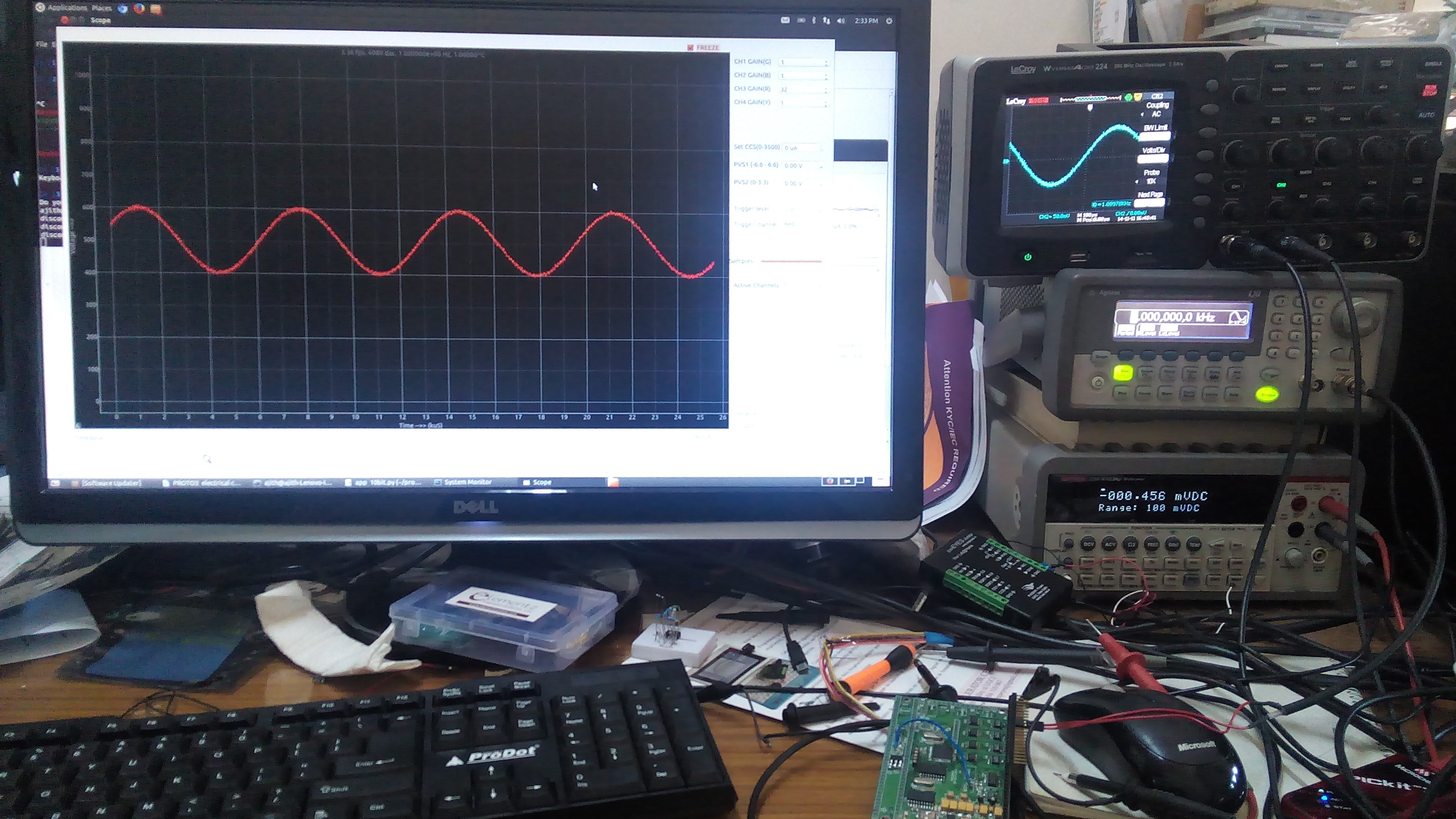
05/27/2015 at 09:37 • 0 commentsReplacing the PGA Vref drivers with TL08 ICs fixed the previous problems. Tested all gain ranges by sweeping frequencies of sine and square inputs across the entire bandwidth, and monitoring the output on a scope. A function generator by Agilent was used to provide the input waveforms.
![]()
A simple laser cut enclosure was also made.
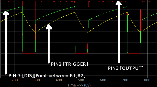
The picture below shows a 555 oscillator being studied using the device. Three oscilloscope channels are being used to monitor the output, voltage across the capacitor, and the midpoint voltage of the two resistors. The results are shown in the next picture.
![]()
![]()
![]() Source: WIkipedia
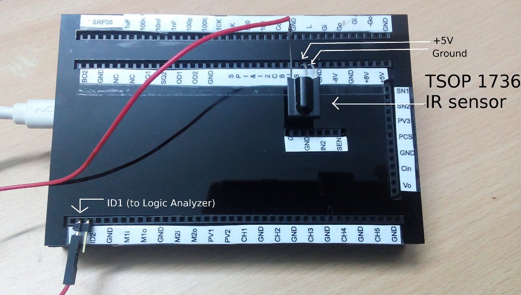
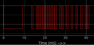
Source: WIkipediaI also started using the Input capture modules along with DMA to try to make a Logic Analyzer at no additional cost. Preliminary results from a TSOP1738 IR demodulator IC receiving the signal from a TV remote are shown
![]()
![]()
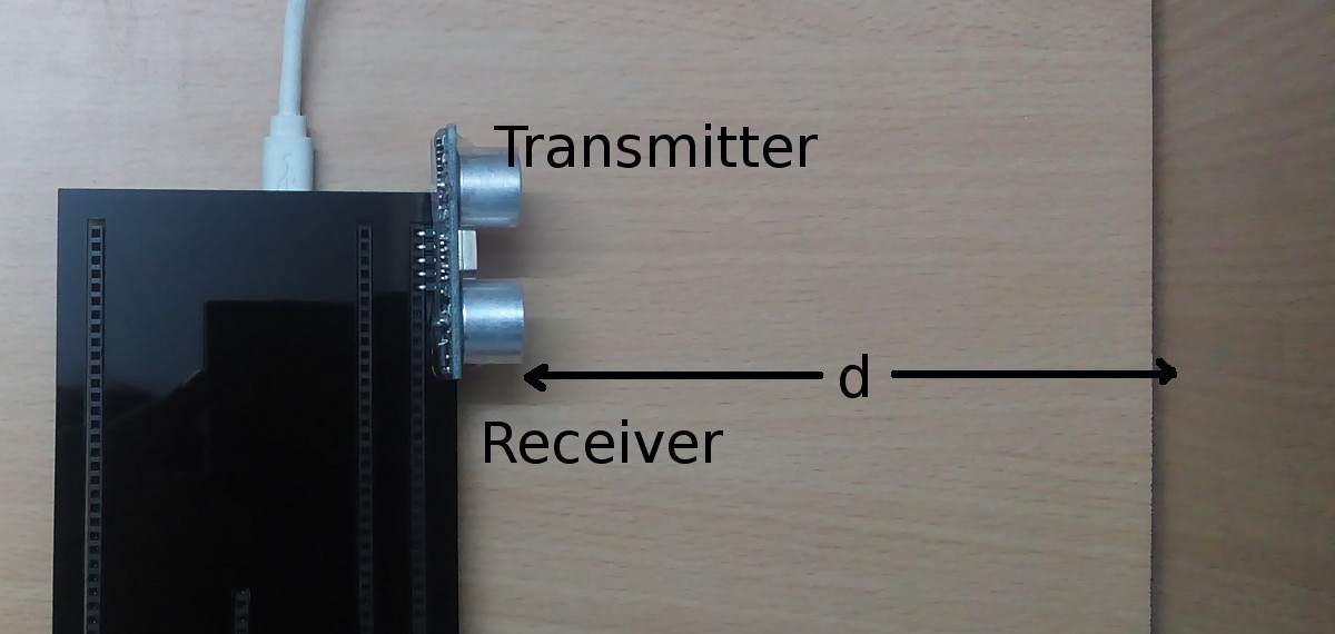
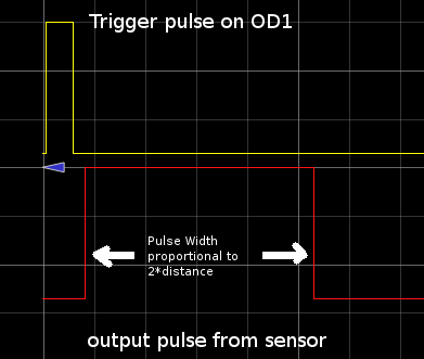
It was also used to test an SR-04 ultrasound based distance sensor
![]()
![]()
Without going into the details of scopes and logic analyzers, I'll post a couple of pictures of both monitoring the same signals.
![]()
![]()
![]()
-
PROTOTYPES #2,#3
05/27/2015 at 08:21 • 0 commentsThe following changes were made
- LM324 was used to buffer a midpoint voltage(1.65) and fed to Vref input of MCP6S21 PGAs. This didn't work as expected in higher gain settings. The datasheet demands an output impedance of <0.1 ohms for Vref, although I'm not sure what caused the erratic behavior. Check out the following image of a 100mV sine wave amplified 32x. The PGA works fine up to 10x.
![]()
- The yellow trace is a mess! The other traces represent high impedance inputs that were floating, and probably accumulated charge which drained once the scope started digitizing them.
- I tried several possible solutions including disconnecting three PGAs and letting the LM324 drive the Vref of only one. But with no hope. Here's what the Vref pin looks like on a LeCroy scope.
![]()
- The LM324 simply cannot drive the Vref at high gain settings.
- Switching to a TL08 worked.
![]()
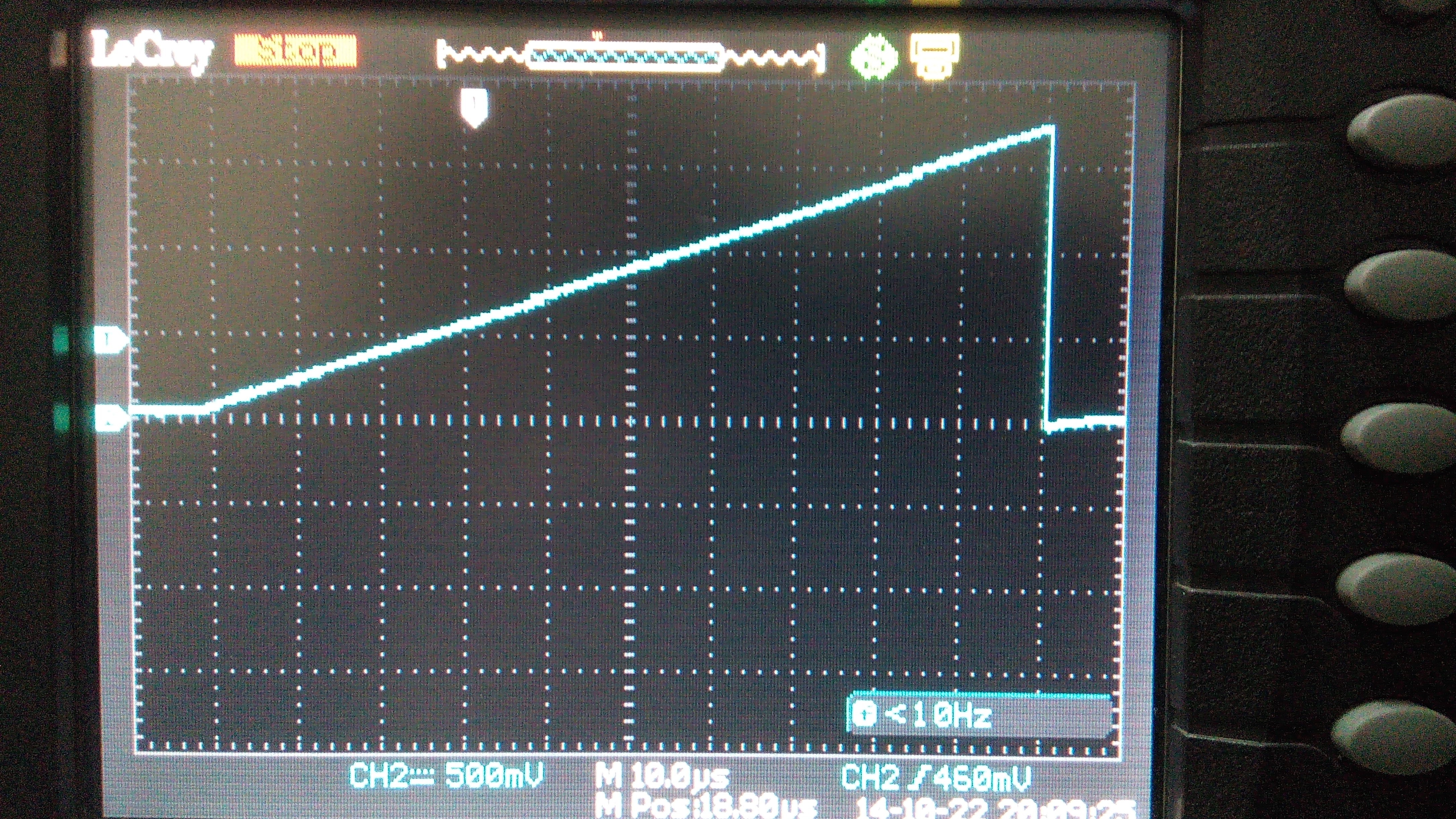
Yellow trace - DAC output to CCS circuit. Blue trace - Voltage drop across a 100 ohm load connected to CCS. The range of the constant current source is dependent on the load resistance since for higher loads, higher voltages need to provided to maintain the same current (I=V/R) , and there;s a limit to that.
![]()
testing an LM311 based tank circuit driver to use as an inductance meter.
![]()
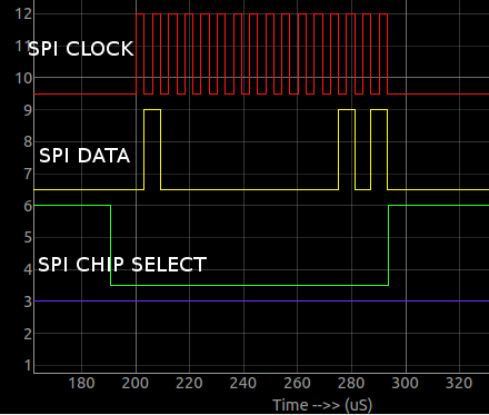
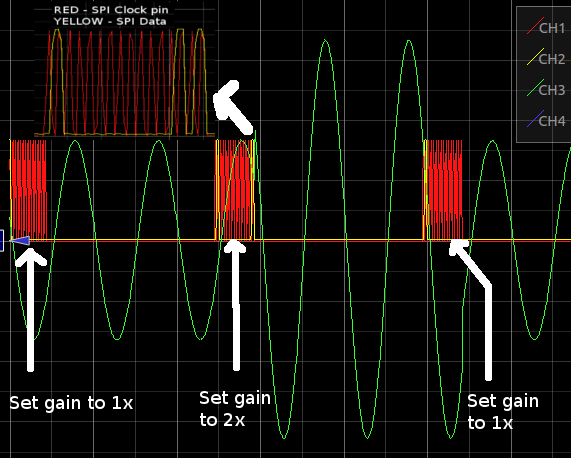
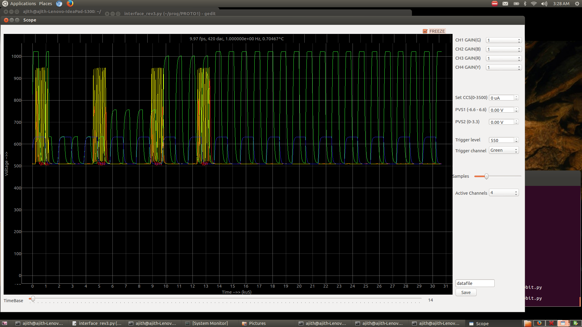
Verifying that other function calls can be executed while the oscilloscope runs in the background. In this instance, The yellow and red traces are looking at the SPI clock and data pins, while the green is a square wave connected to a PGA. The data sent over the SPI bus is actually changing the gain of that particular PGA. One can see that once the last clock of each packet is sent to the PGA, its output(green trace) changes.
![]()
Vdd (Yellow) , AVdd (Blue) rising together since a diode was connected from Vdd to AVdd. No PIC oscillator failures have occured since.
![]()
Aluminium Capacitors can't seem to do the job for the charge pumps. They require low ESR Tantalum capacitors.
![]()
I monitored a capacitor's voltage while the CTMU was being used to estimate its capacitance using constant current charging. Q=CV => I*t = C*V [ Current, and charging time are both set by us. Voltage is measured at the end of the charging time, and therefore Capacitance can be calculated. ]
Monitoring this charging cycle using the LeCroy scope caused an increase of 13picoFarad in the measured capacitance. This value somehow tallies exactly with the 13pF capacitance specified on the LeCroy scope. No current source calibration was used.
![]()
Trying out a NanoAmmeter. The LED is used as an input source, and the output from the ammeter goes up by a few mV when I shine a light source onto the LED
-
Prototype #1
05/27/2015 at 08:08 • 0 commentsThe very first board .
![]()
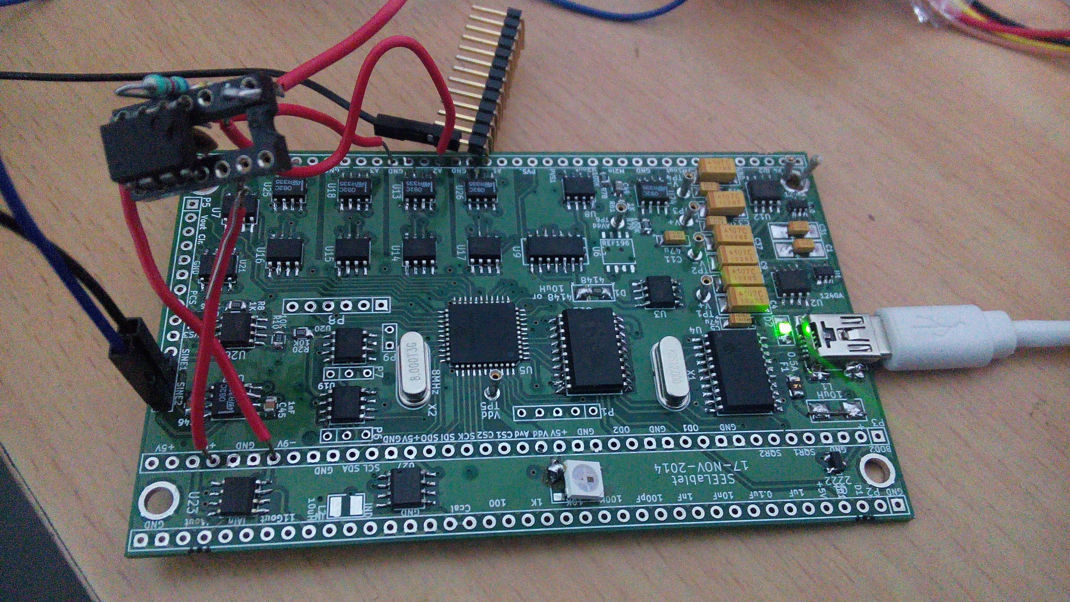
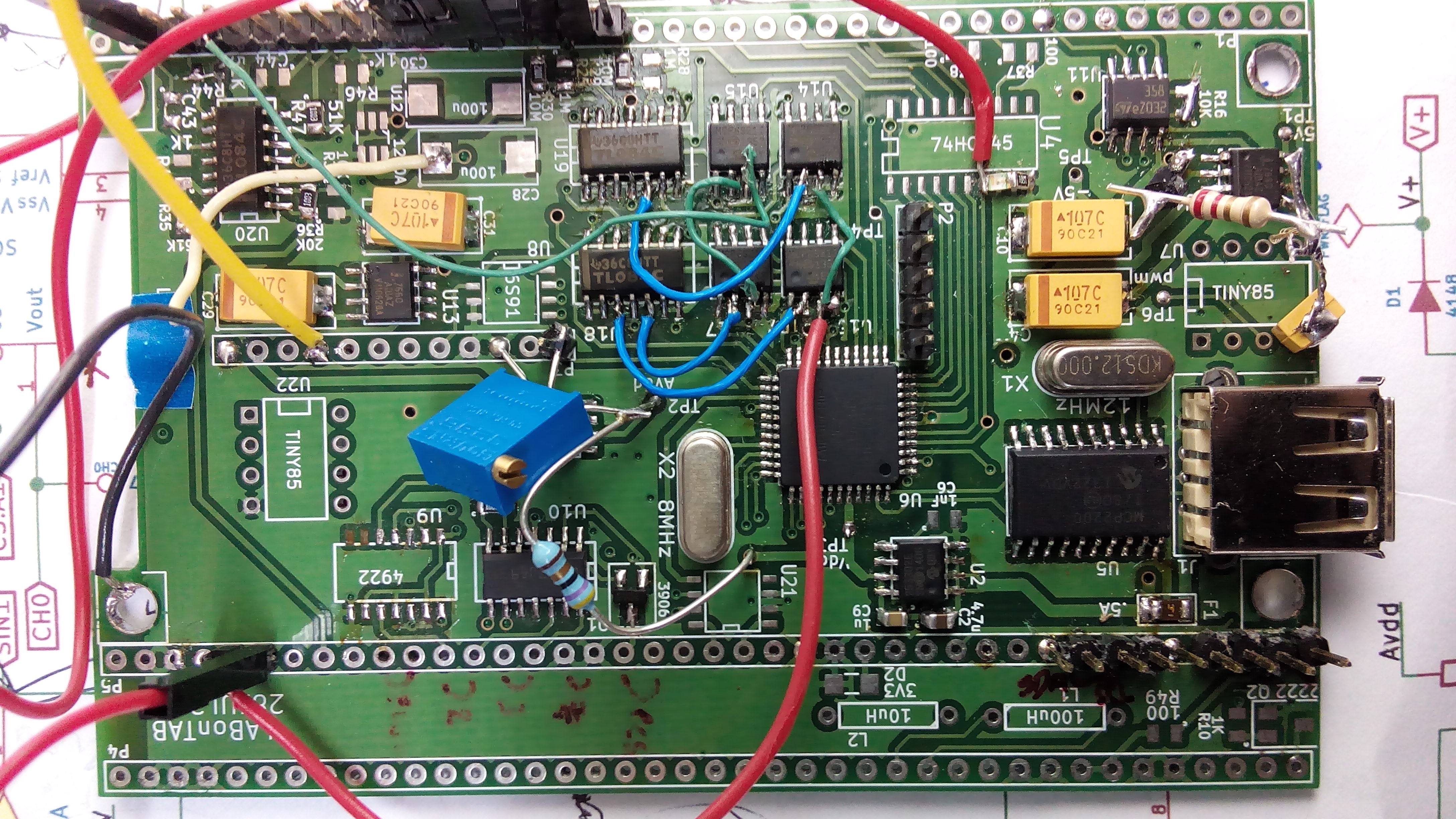
A lot of patchwork went into this
Rough list of features:
- USB powered. .5mA polymer fuse. MCP2200 convertor.
- Controlled by PIC24E
- MCP1725 LDO regulator
- REF196 stable 3.3V voltage reference
- bipolar power supplies generated by 7660 and 1240A charge pumps
- MCP4922 2-channel DAC for programmable voltage and current sources
- MCP6S21 programmable gain amplifiers to provide several software configurable input ranges for voltmeters and oscilloscopes.
- 4-channel oscilloscope. +/- 16V full range. +/-500mV at 32x PGA gain.
- ATTINY based sine wave generator
- Capacitance measurement via CTMU of PIC24E
- Digital I/O
- Component store - A collection of commonly used resistors, capacitors, diodes etc soldered directly on the PCB, and broken out into a berg strip for quickly trying out stuff.
Errors and concerns that decided the design of the next iteration
- The voltage reference of the PGA needed to be set to the midpoint. LM324 buffered midpoint references were added.
- Quality of ATTINY generated sine wave was rather poor. I found a low priced alternative, PIC1572, which not only ran faster, but also had 3 16-bit PWMs, and a 5-bit DAC which could be used to add more programmable voltage and current sources.
- Planned to use two PIC1572 to the next iteration for generating dual sine waves. Made the mistake of assuming the outputs would be phase correlated since they were identical. :/
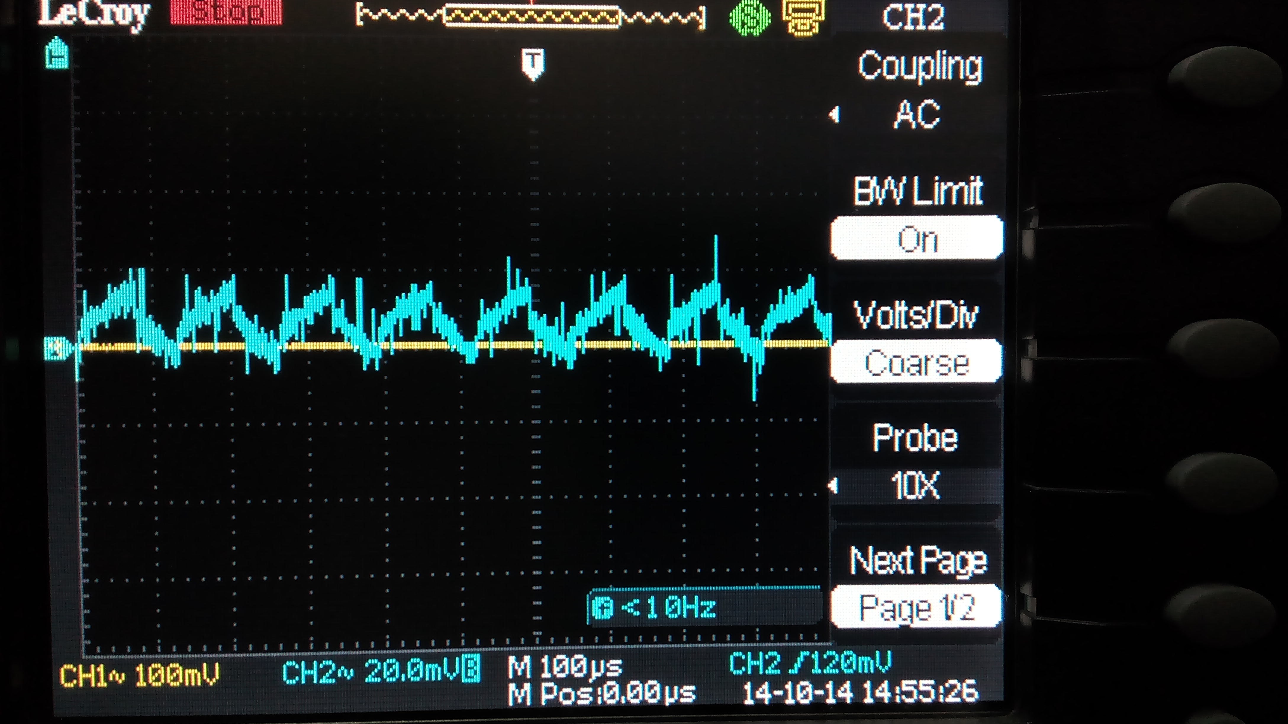
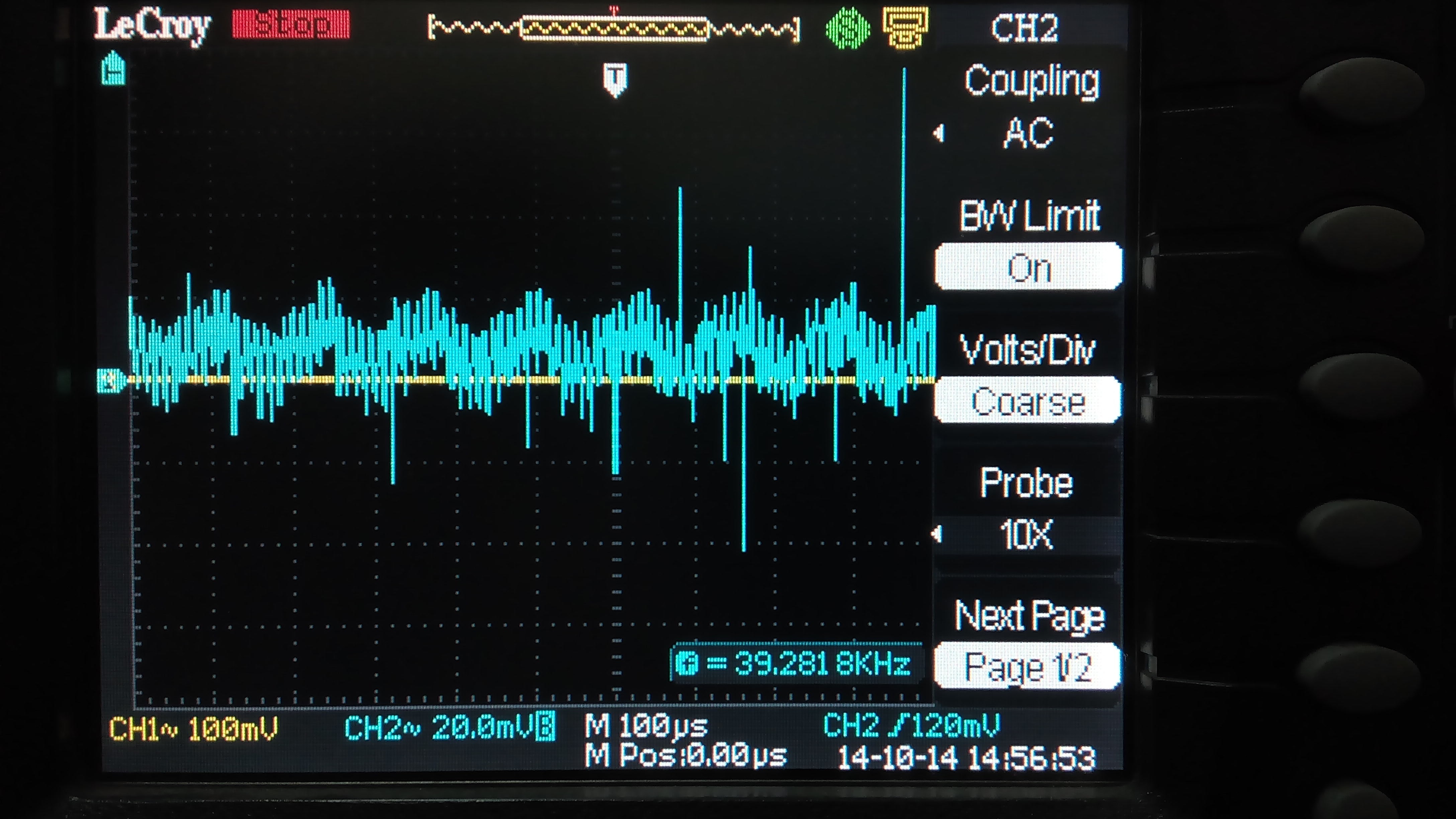
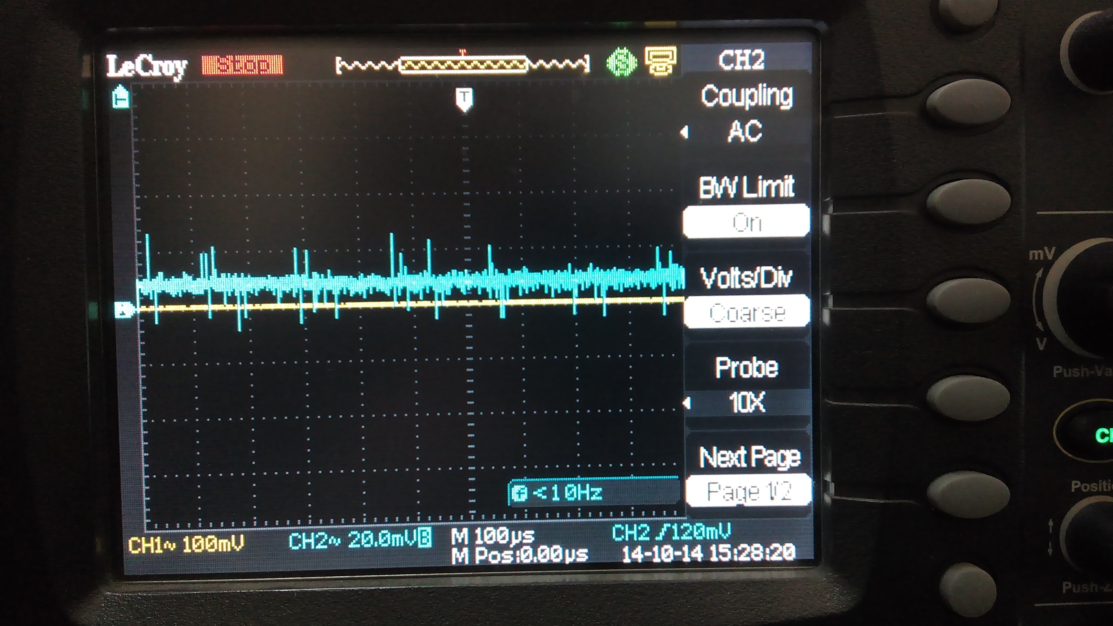
- Ripple noise from charge pumps needed additional filtering.
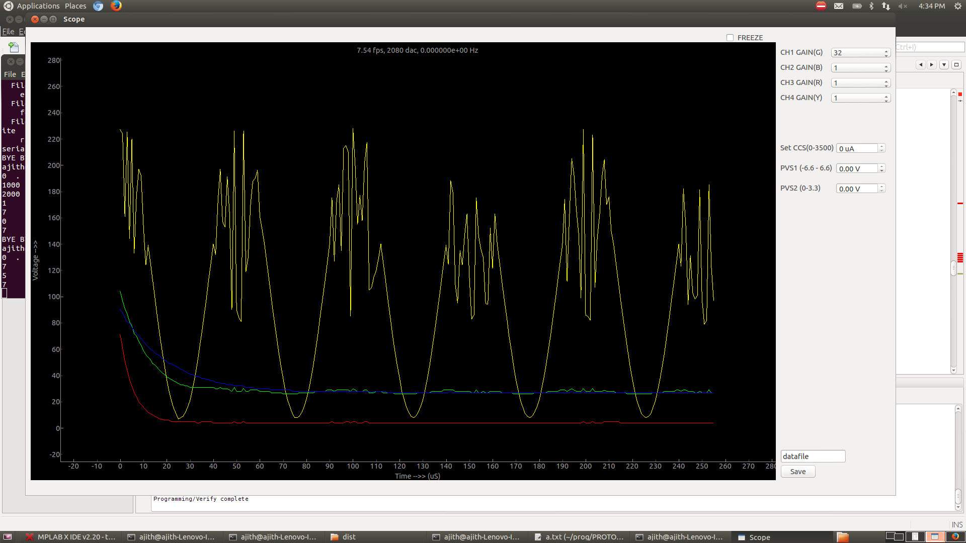
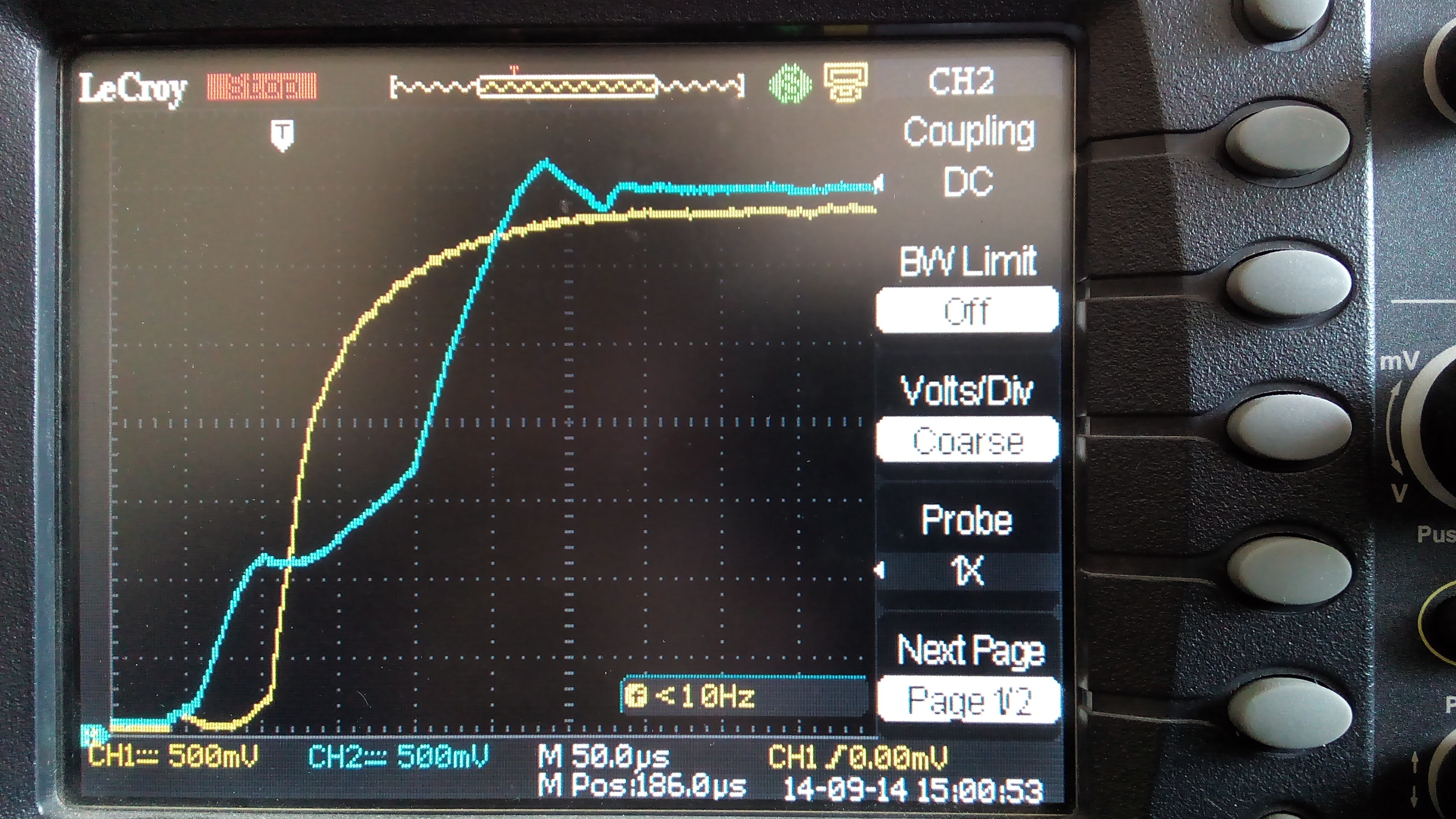
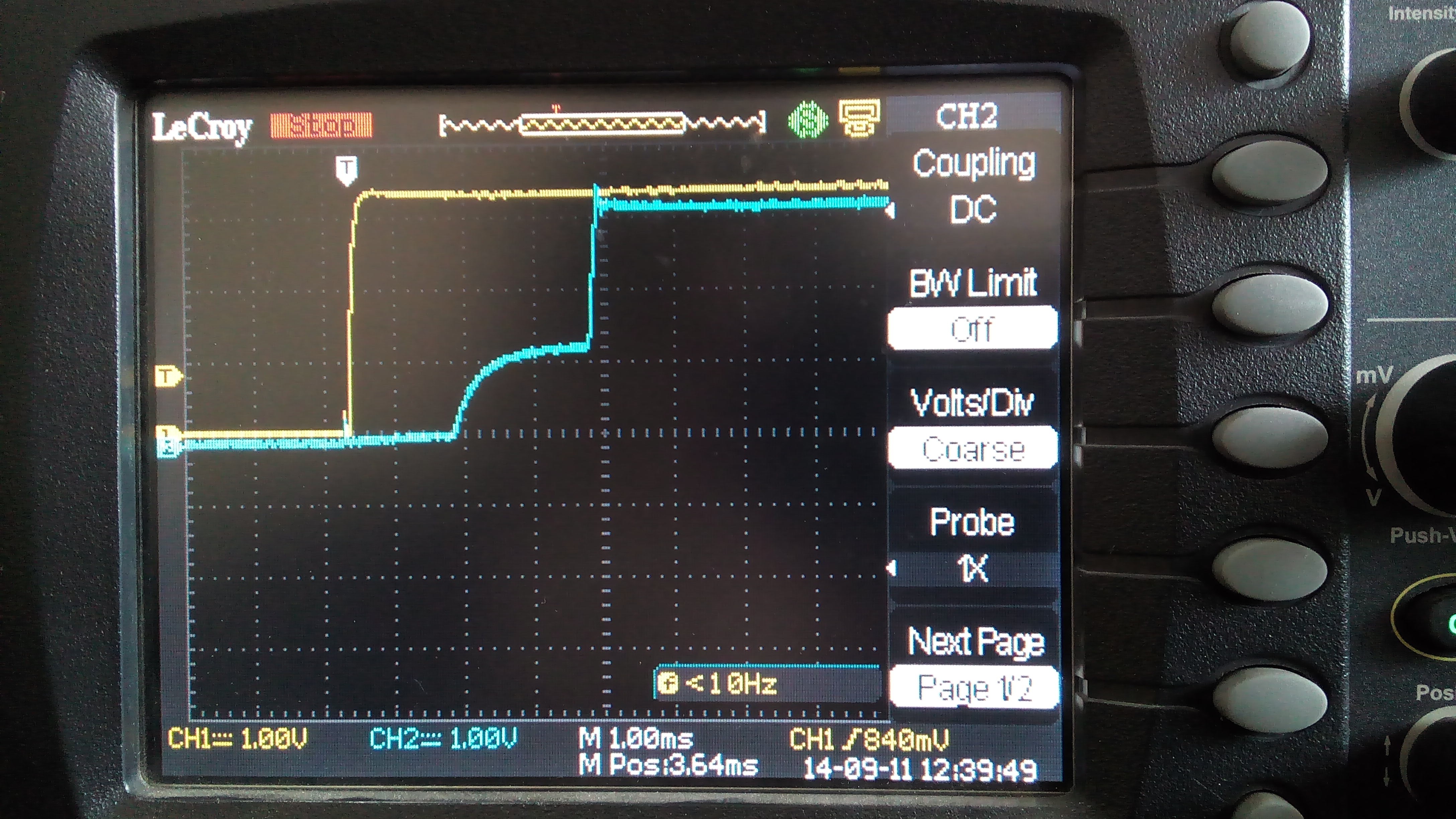
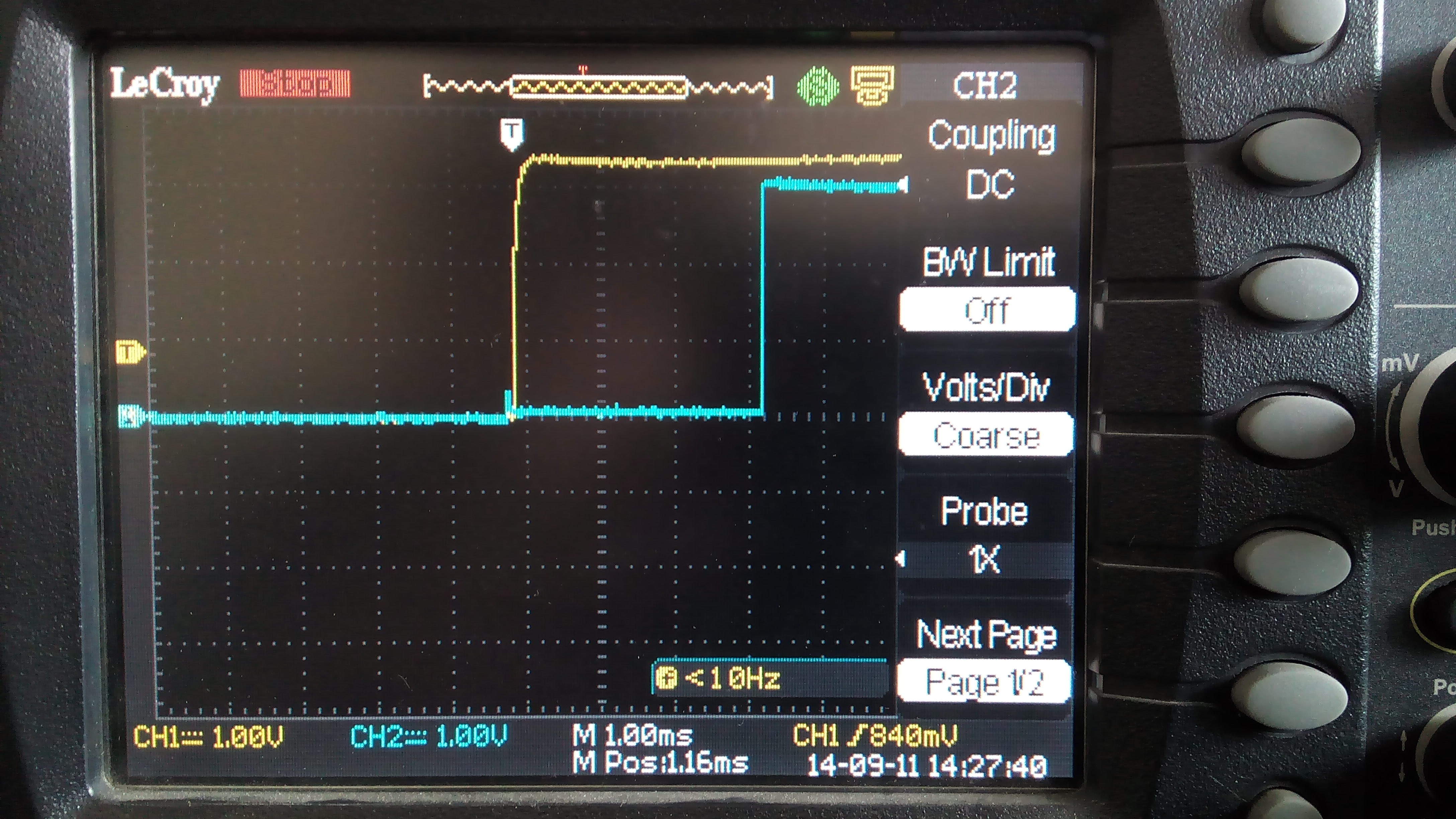
- PIC24E refused to START . I had powered Vdd from the MCP1725, and Avdd from the REF196 for separating analog and digital sections. After much hunting around, I found that Avdd and Vdd must never be more than 300mV apart or else the oscillator won't start. I tried to delay the Vdd rising speed by trying out several capacitors attached to its Delay pin, but with no luck. Here's a screenshot detailing how the Vdd(blue) and AVdd(yellow) voltages would rise on power up
![]()
The Cdelay Pin of 1725 was attached to a 1nF cap.
In this instance , Yellow is Avdd, and Blue trace is the PWRGD output of 1725. It seemed I couldn't get them to rise together. Finally I settled on a a diode that would keep the two within a certain range of each other. Once both have risen to their full 3.3V level, the diode can be removed with no consequence. Have had no problems since.![]()
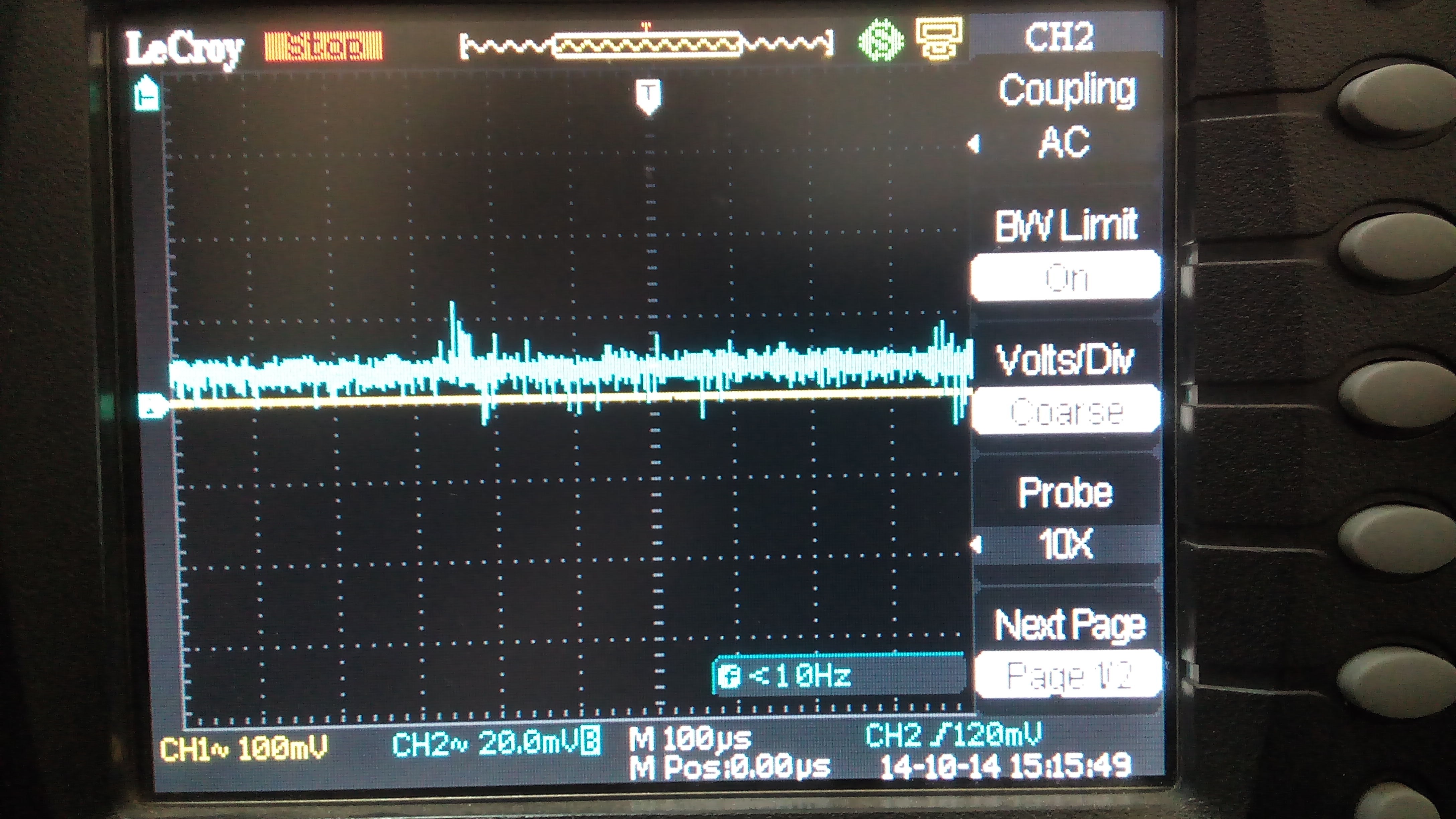
Noise Levels
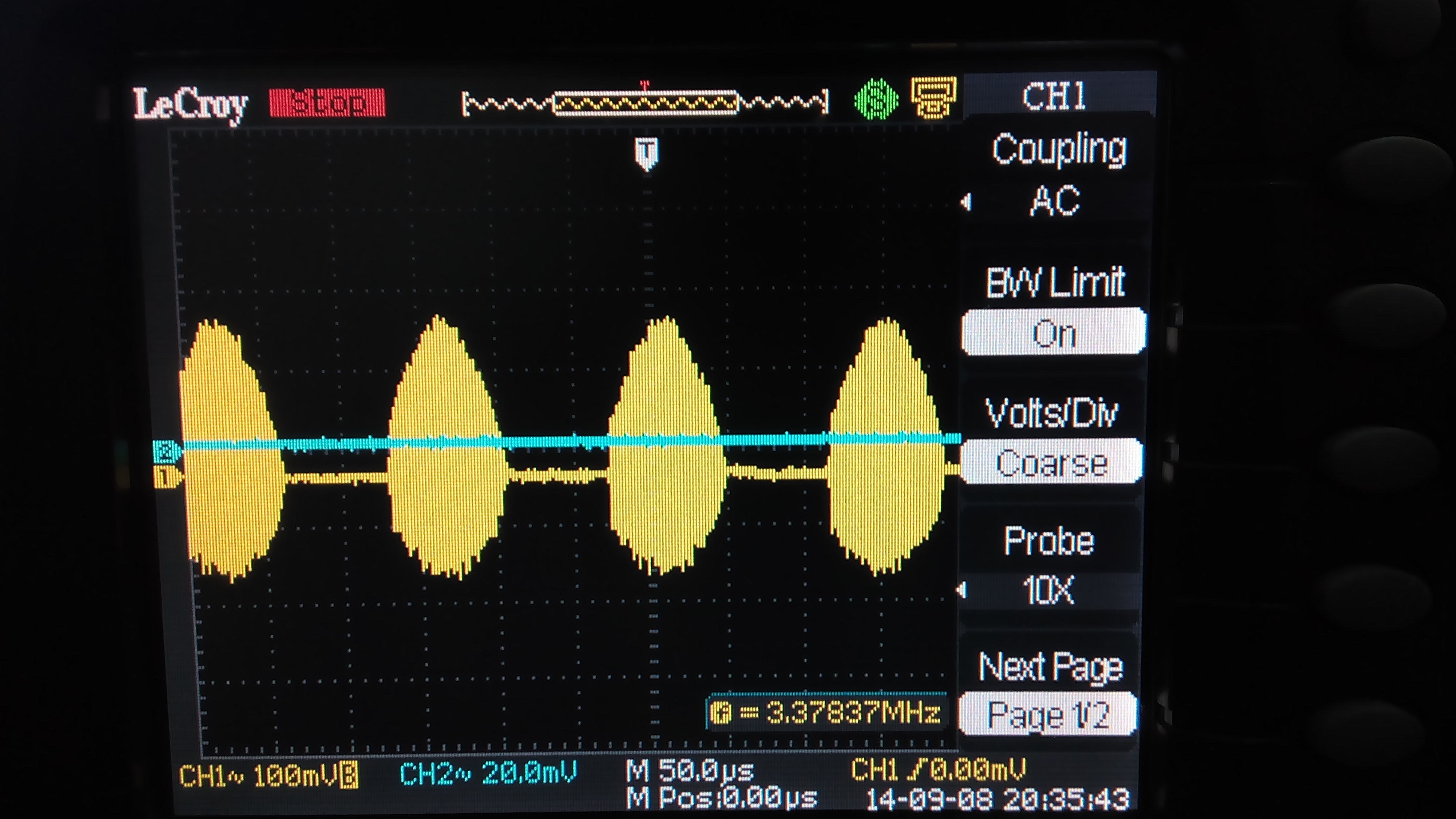
Negative power supply(-10V voltage inverter) ripple level with a 680 ohm load.![]()
![]() Positive power supply (+10V voltage doubler) ripple level with a 680 ohm load.
Positive power supply (+10V voltage doubler) ripple level with a 680 ohm load.Attempting to Clean noise with RC filters
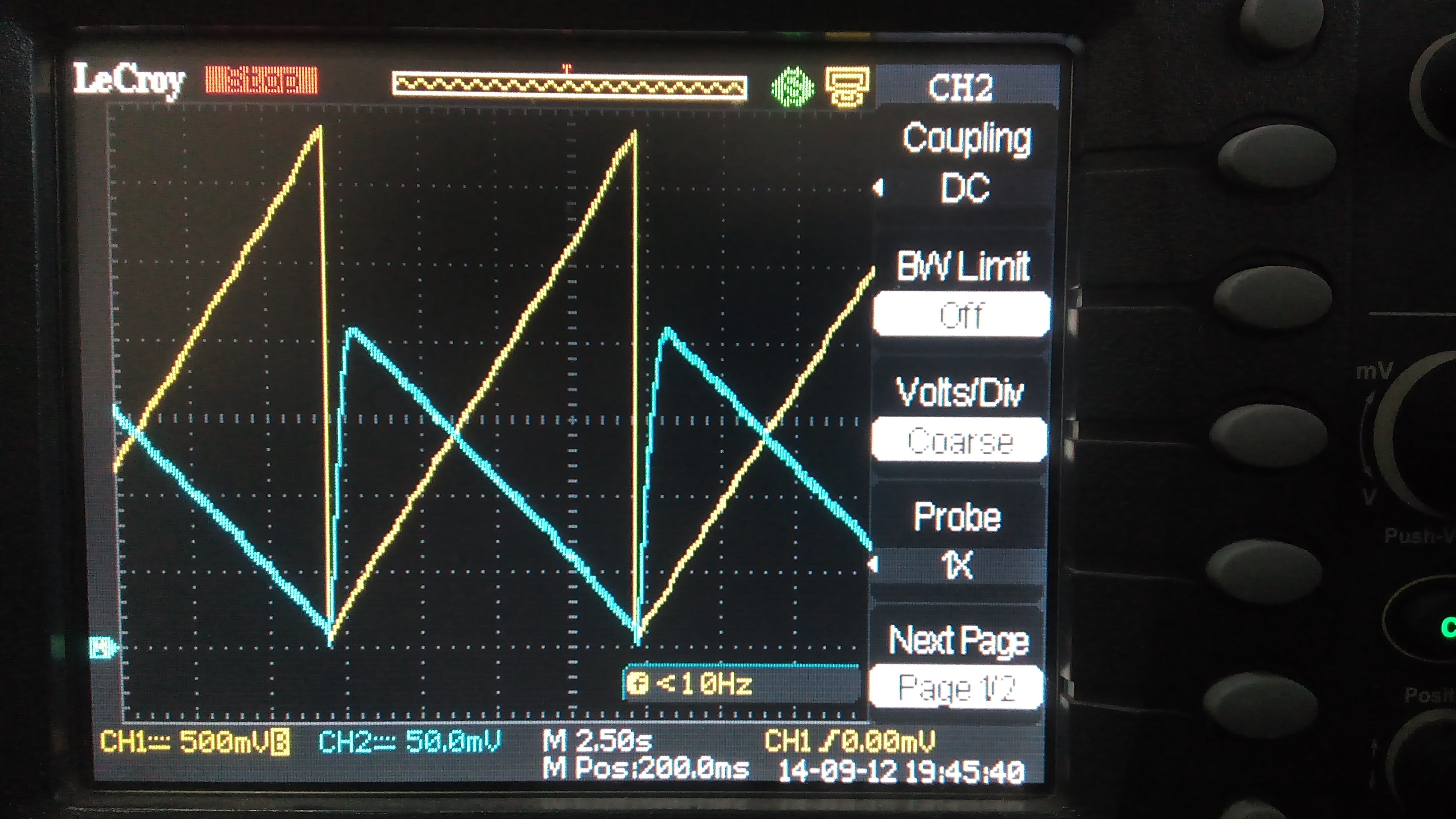
![]() 25 uF, 47Ohm RC filter applied to +10V
25 uF, 47Ohm RC filter applied to +10V
100 uF, 47Ohm RC filter applied to +10V![]()
![]()
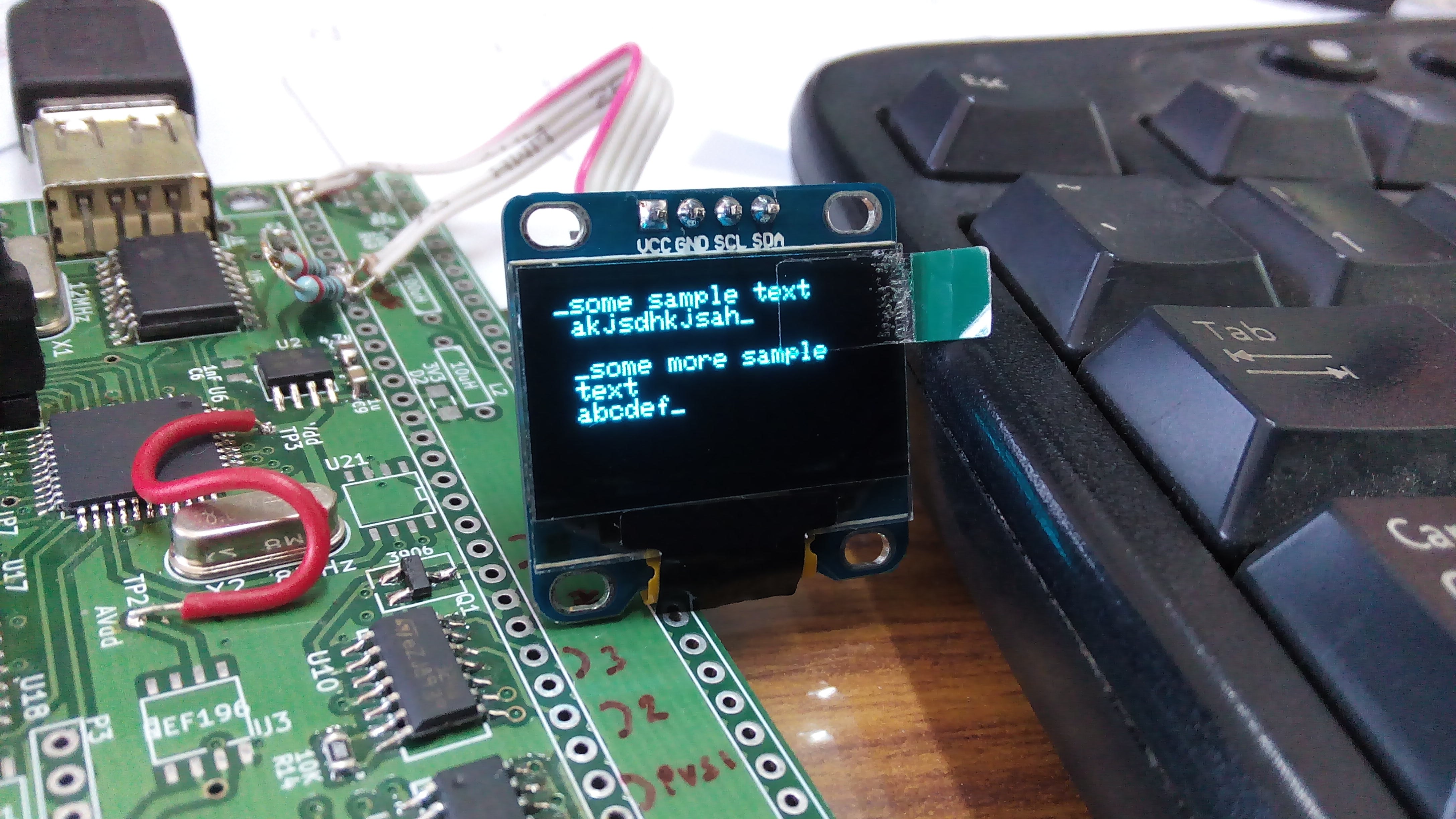
Tested I2C with SSD1306 OLED display
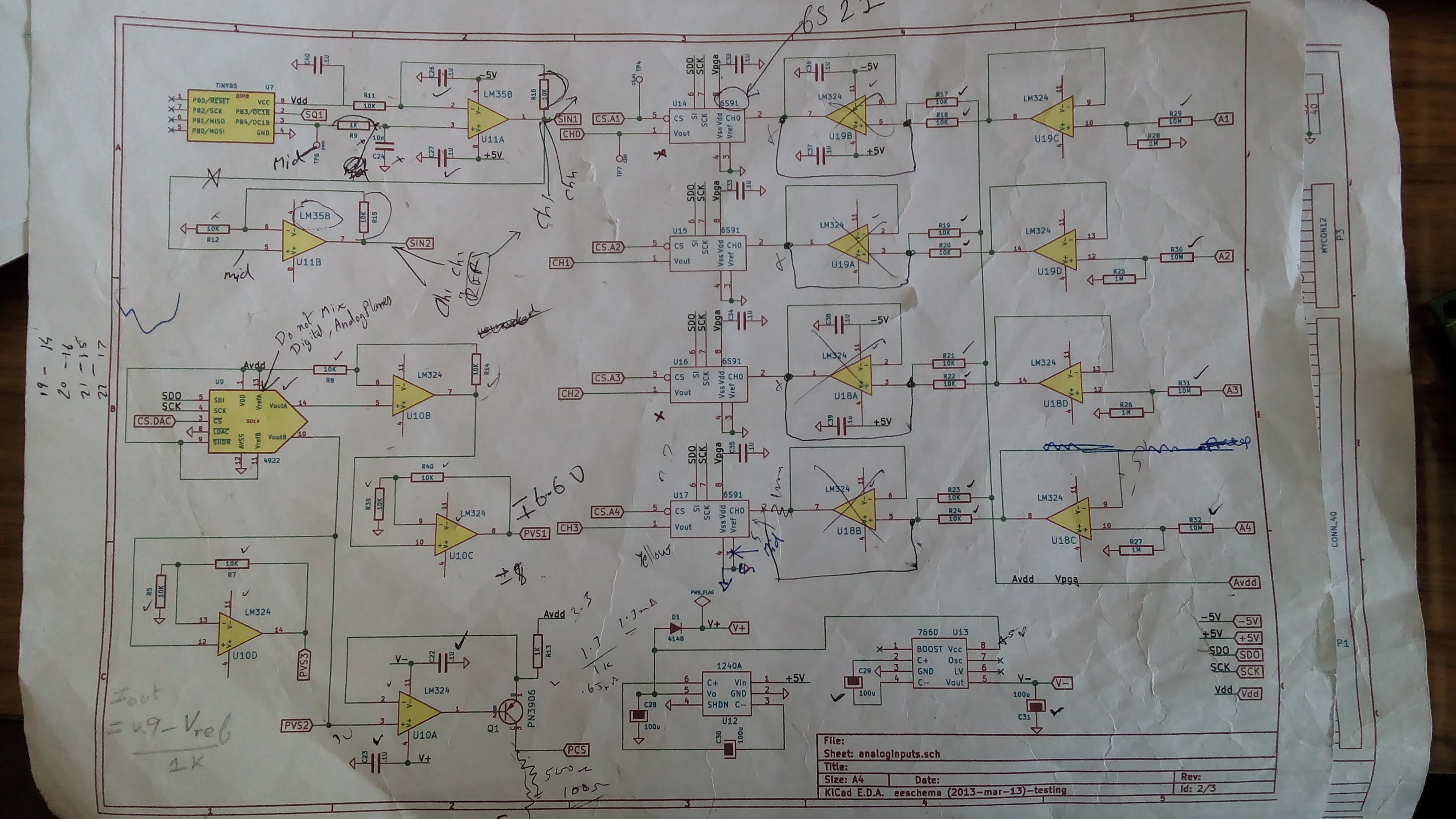
'Corrected' schematic. page#2![]()
![]()
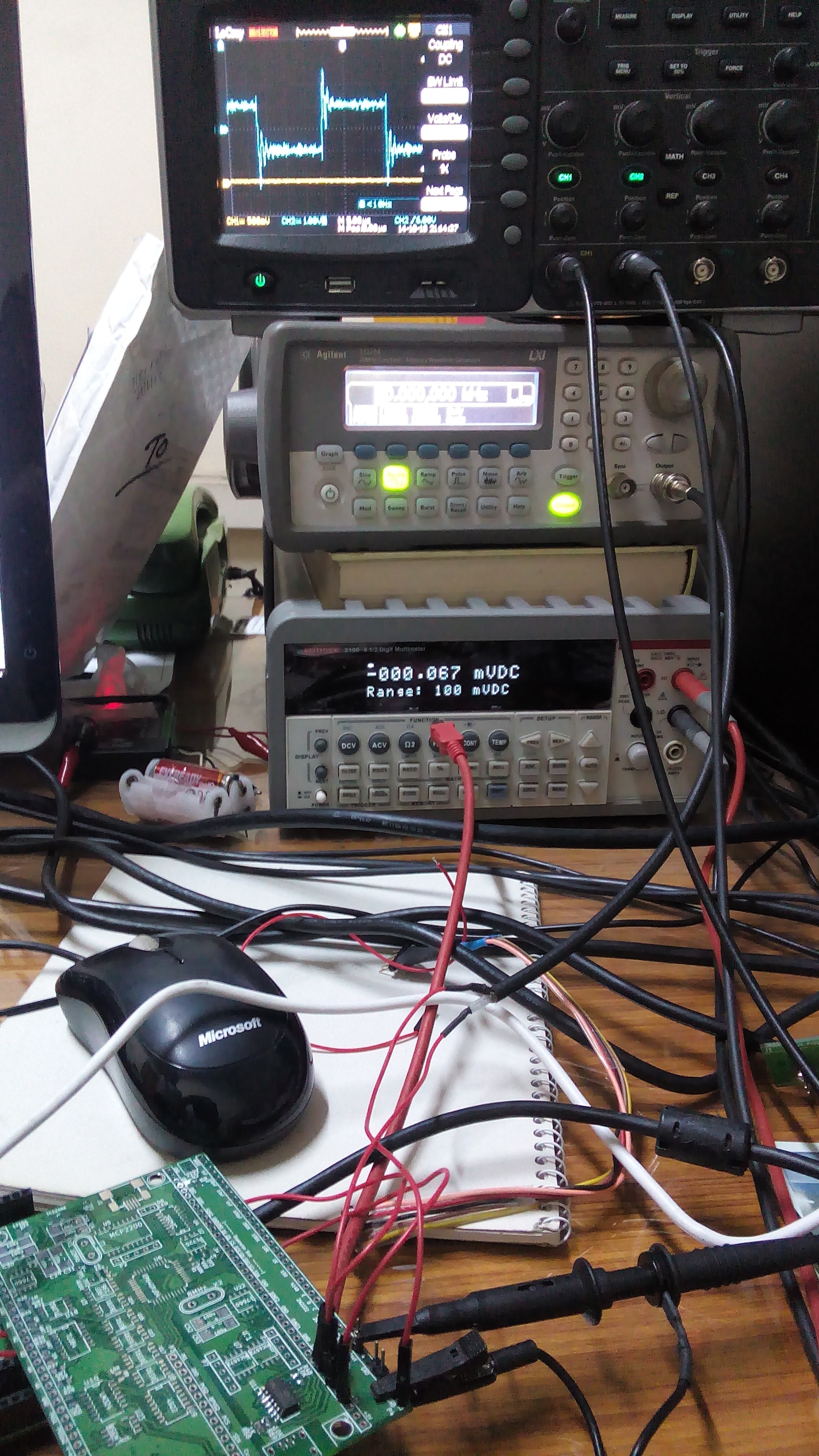
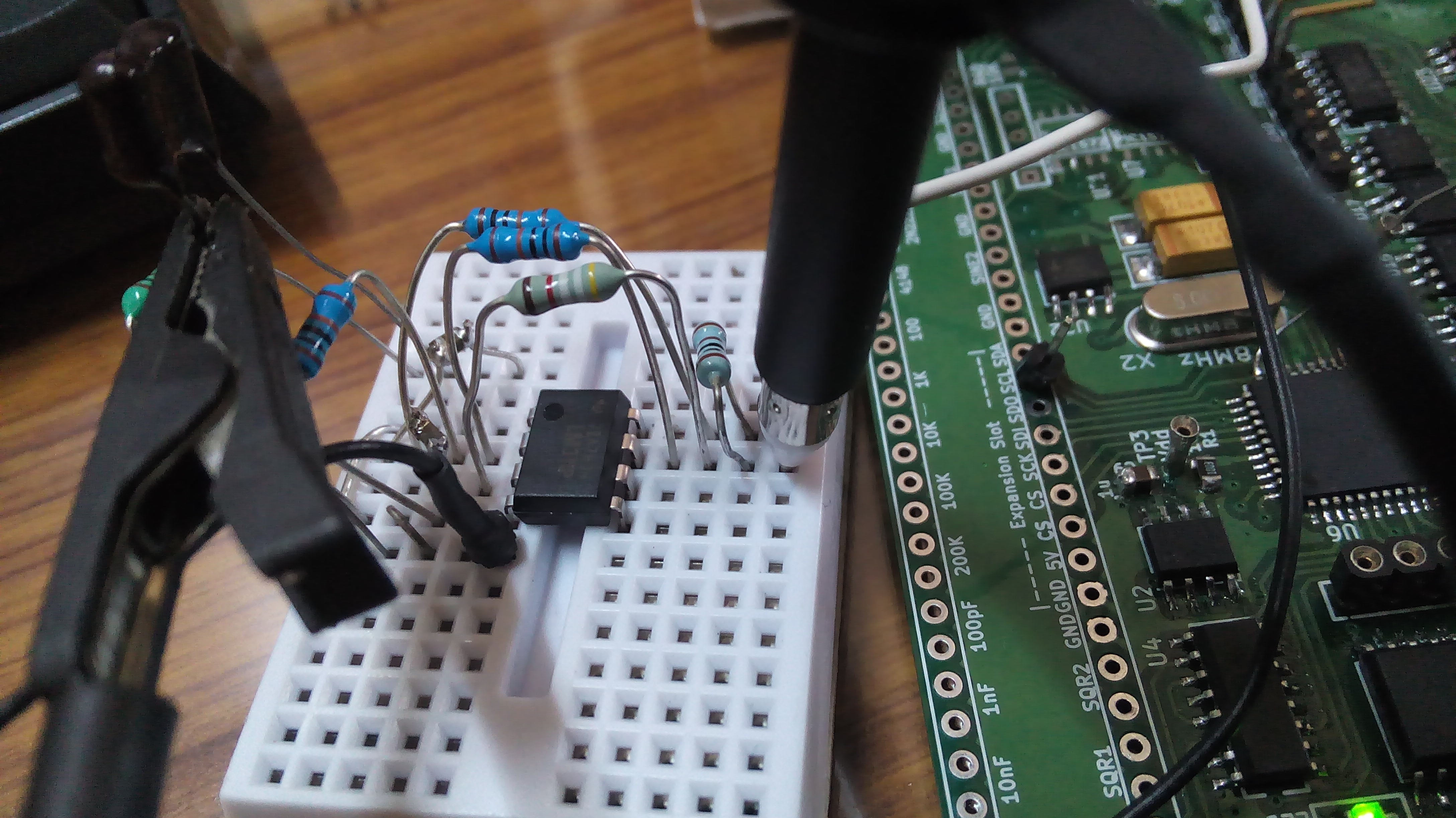
Testing an inverted configuration op-amp for input voltage range. Overshoot with oscillations occurs if frequency compensation isn't set up.
Python Powered Scientific Instrumentation tool
A multi purpose lab tool accessible by simple Python functions, and capable of studying a wide range of physical phenomena.
 Jithin
 Source: WIkipedia
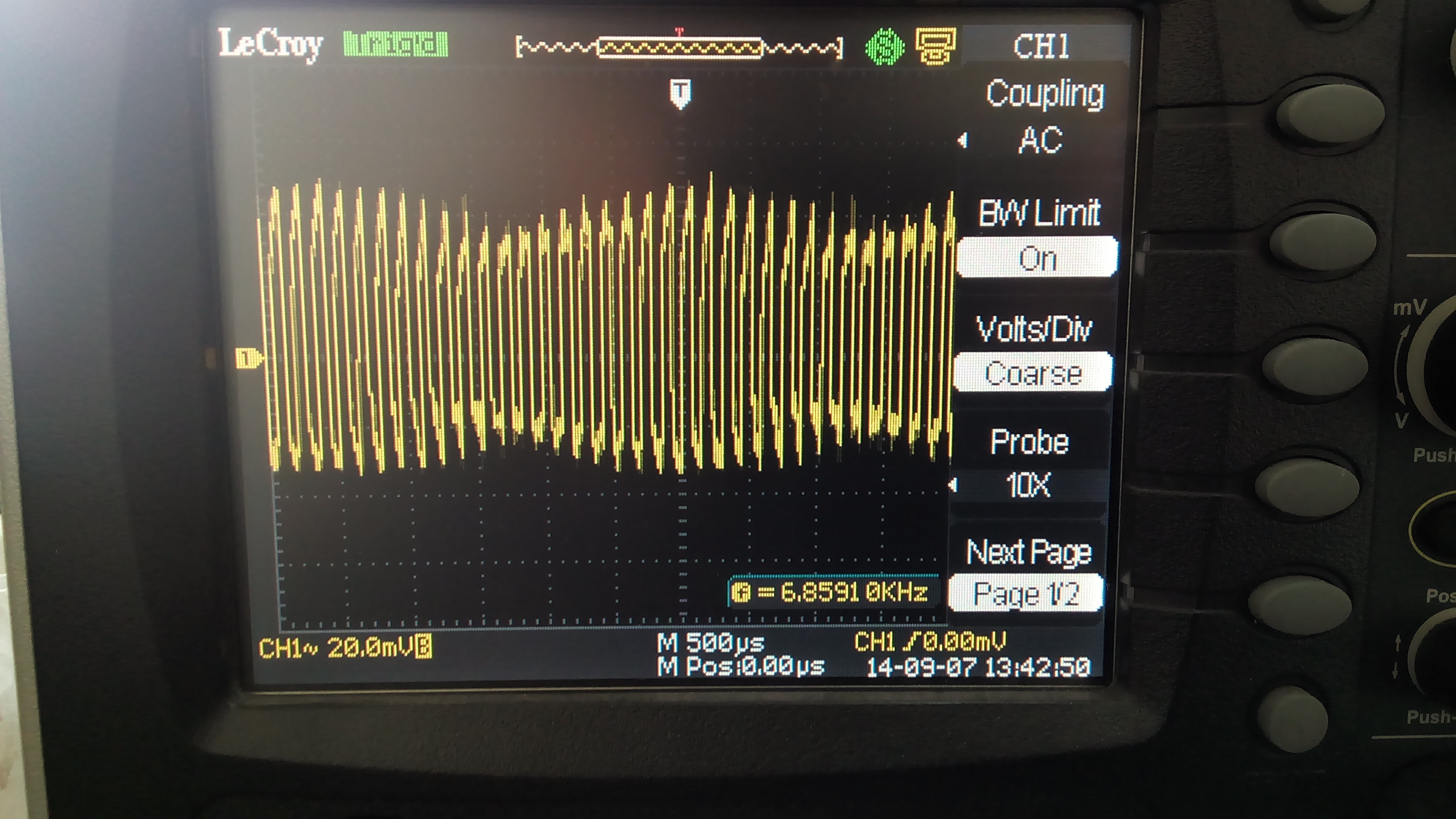
 Positive power supply (+10V voltage doubler) ripple level with a 680 ohm load.
 25 uF, 47Ohm RC filter applied to +10V