-
LED blink without CPU
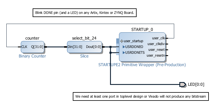
02/04/2016 at 18:39 • 0 commentsFor simple LED blink, we can use internal clock and forget totally that there is a hard processor available. This design work equally well on any Artix, Kintex, Virtex or Zynq board!
![]()
If we want to write the Blinky in VHDL, then this is equally easy:
![]()
We send the clock to output port, and create wrapper that is not managed, then we can just write normal VHDL. Of course we could just instantiate the startup directly in VHDL too.
library IEEE;

use IEEE.STD_LOGIC_1164.ALL;

library UNISIM;

use UNISIM.VCOMPONENTS.ALL;

entity blink_top_wrapper is

  port (

    LED : out std_logic

  );

end blink_top_wrapper;

architecture STRUCTURE of blink_top_wrapper is

  component blink_top is

  port (

    clk66mhz : out STD_LOGIC

  );

  end component blink_top;

signal clk: std_logic;

begin

blink_top_i: component blink_top

     port map (

      clk66mhz => clk -- this is free running clock from BD

    );

    -- LED is steady on!

    LED <= '1';

end STRUCTURE;
This is basically the vivado generated wrapper, 3 lines changed.
![]()
This design takes the clock from PS PLL, from FCLK0. This design only works if Zynq CPU has executed the FSBL (first stage bootloader). Again we can use this clock from the PS PLL in our plain VHDL code.
-
Production in progress
09/11/2015 at 07:30 • 0 commentsAll PCB from first PCB batch are being assembled, availability announced soon.
-
Parallax Propeller 1 emulation in FPGA
08/19/2015 at 18:24 • 0 commentsIT is working now
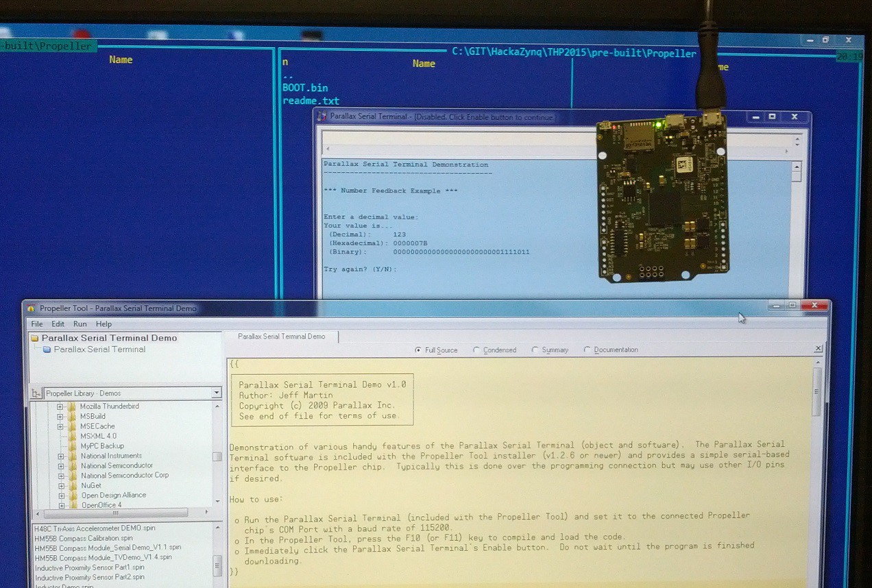
Zyn PS Block is only supplying clock into FPGA not used otherwise, all the work is done by the Propeller Soft Core implemented in FPGA Fabric.
Prop P31, P30 are connected to FTDI USB UART, P0..P15 to Arduino D0..D15
![]()
binaries on github, but need to FLASH them, they would not work if loaded from SD Card.
HOWTO
- get the BOOT.BIN from github
- Write to flash, reset or replug usb
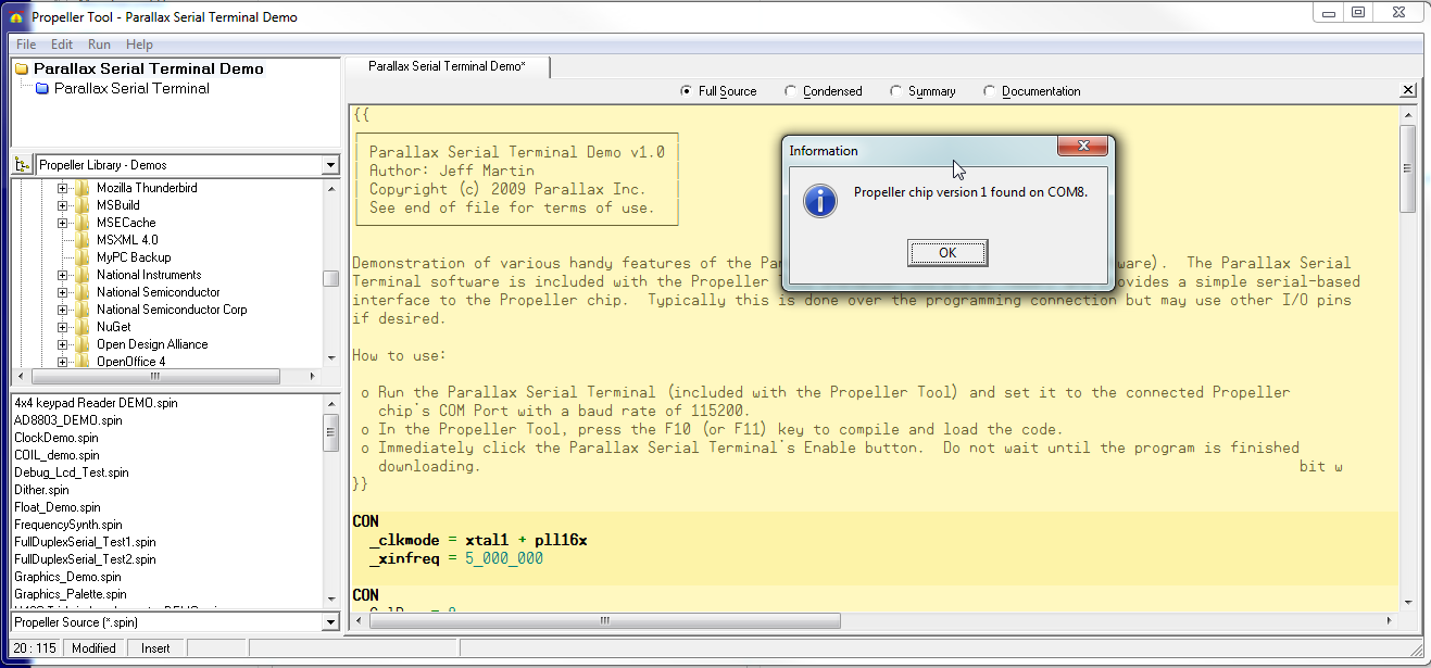
- start Parallax Propeller tool
- Press F7
Should identify Propeller version 1
![]()
-
Flashing for linux boot
08/18/2015 at 21:28 • 0 commentshttps://github.com/AnttiLukats/HackaZynq/tree/master/THP2015/pre-built
there are BOOT.BIN and image.ub
call C:\\Xilinx\\SDK\\2015.2\\.\\bin\\zynq_flash.bat -f BOOT.bin -flash_type qspi_single
this will update the Flash with BOOT.BIN
note: BOOT.BIN includes: FSBL (first stage bootloader, FPGA bitstream and u-boot)
From flash only FSBL is loaded, then this FSBL loads from BOOT.BIN on SD Card
FPGA bitstream
u-boot
executes u-boot,
after that u-boot would load linux image from image.ub
note: it is possible that terminal does not accpept input, please close and open putty, this should help, there seems to be a issue that some terminal program go nuts if the say some garbage during FPGA config. We are working on this..
-
files to github
08/17/2015 at 18:56 • 0 commentsfull hardware design, CAD sources and generated files too
-
Linux 3.19
08/14/2015 at 15:30 • 0 commentsboot OK, the memory size is visible: 64MByte
![]()
-
Vivado Board Awareness
08/10/2015 at 14:21 • 0 commentsTwo days of frustration, it seems that Vivado 2015.2 has an BUG related to PS presets and Board Part flow, as soon the system has been configured with LPDDR2 then the board files and presets become invalid. So we have fail a WebCase by Xilinx for this.
It is not a shows stopper, it is possible to provide the presets and board files with LPDDR2 not enabled, and then later apply the required setting per hand.
-
16 Channel Frequency Counter
08/02/2015 at 12:03 • 1 comment16 Channel Frequency counter, the easy way:
Step 0:
Start Vivado, Create project, Create new Block Design.
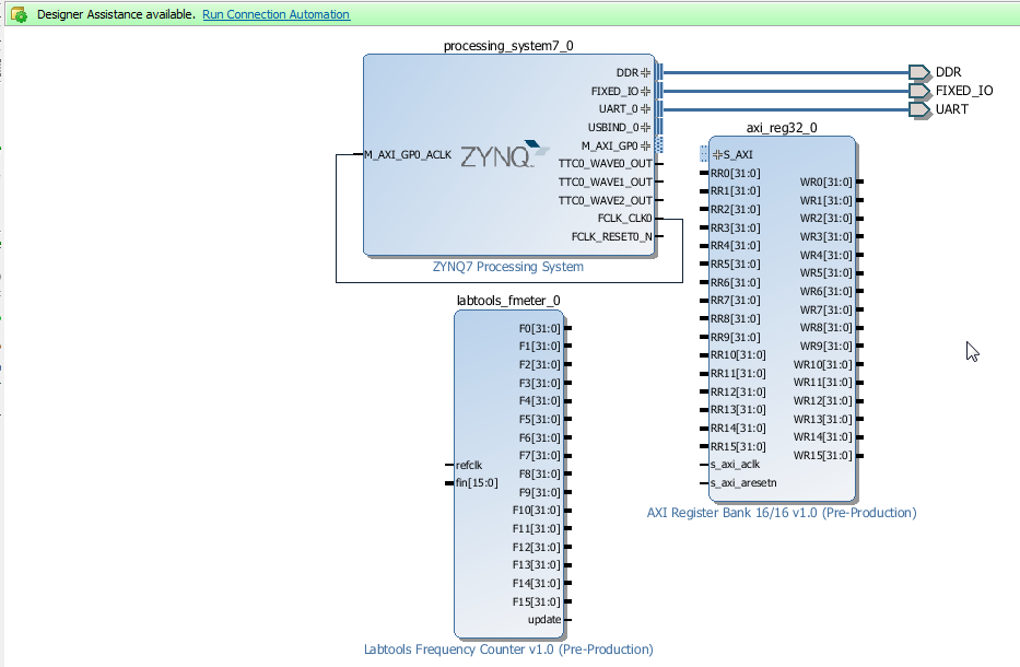
Step 1:
Type freq.. and let the drop down to populate, then select the IP Core to be added:
![]()
Press Enter!
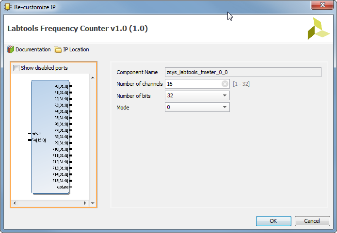
Step 2:
Doubleclick and set number of channels to 16
![]()
Press Enter!
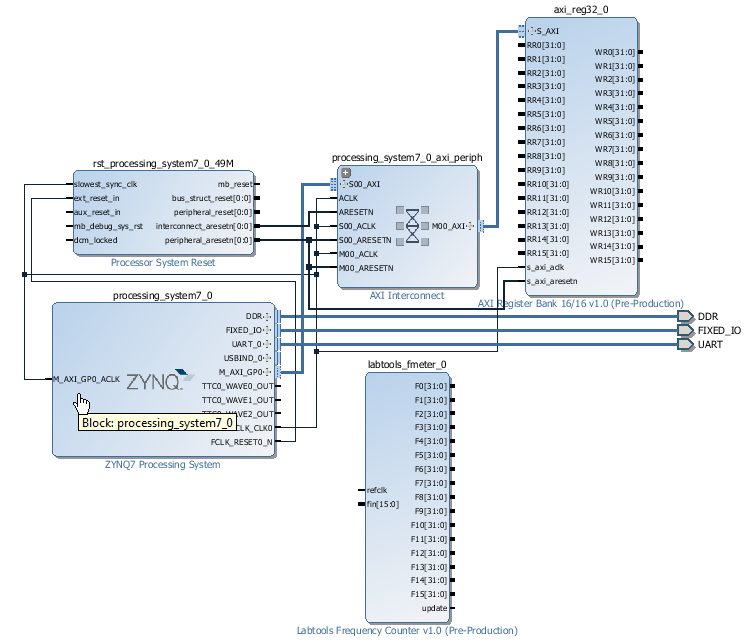
Step 3:
Add AXI Register Bank, the Block diagram should look like this:
![]()
Step 3:
Click on the "Run Connection Automation! Click on OK!
![]()
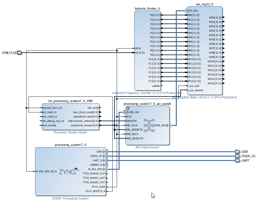
Step 4:
Connect Frequency meter outputs to the register inputs, then connect the ref clock to Fabric Clock output from PS7 Processing Block, and make the Frequency meter inputs external, this is all done by a few mouse-clicks.
![]()
Step 5:
The Hardware is now ready for build, before final bitstream generation we would need to assign the DIN[..] pins to actual pins in the Arduino headers. After that we can close Vivado and continue with Software.
Step 6:
For quick test without Software, Vivado labtools VIO can be used:
![]()
Frequency meter in action, D2 in Arduino header was connected to test clock with 33MHz
This Frequency meter was used on the "zynq arduino" board during proof of concept testing of LiLi (Light Link) where a DDS was usd to generated the LED blink rate and the "frequency meter" IP Core did display the Frequency..
This is Free IP Core, and if not yet published soon will be. It is fully ready for Vivado IP Core repository.
-
Cost optimization, run 1
08/01/2015 at 10:17 • 0 commentsPCB Rev 1 are working and usable but there is room for BOM cost optimization. Current sale price could be 89 EUR, with extensive BOM optimization it could be lowered - hopefully.
USB micro-B to USB mini change
FTDI USB connector is currently micro-B footprint (was actually mounted with micro-AB what is no go for real production). For some reason micro USB connectors cost much more than mini USB connector. As example chepest mini-USB connector at Mouser costs 0.145 EUR. Micro USB is currently in BOM with cost closer to 1 EUR!
This change requires moving the connector components to make more room, but it is still doable and fits the PCB edge area available.
OP Change
The SOT23-6 packaged Operational Amplifier used for Analog input buffer for the Arduino Analog header inputs was chosen from our standard library, and is priced over 1 EUR. Footprint compatible part from Microchip costs 0.17 EUR only at Mouser. This is BOM change only no PCB change required.
Reset Diode Change
In the reset input we accidentially used almost first diode from our library it happened to be shottky diode in 0201 package, and not the cheapest one. This 0201 Diode is not so loved by SMD assembly operators as it is almost impossible to recognize the polarity marking as the Diode is bare die type, at the top the bare Si die is visible. This change required PCB change as well, PCB space is availabe no issues. Some BOM cost reduction will also come. Lowest cost diode at Mouser is about 0.032 EUR only. The 0201 Shottly Diode does cost much more.
VCC Switch Diode Change
There are 2 diodes in the schematic that are used to separate the power supplies, both list with 0.6 EUR in the BOM, quick search at Mouser shows suitable diodes priced 0.15 EUR.
USB Power Switch
TI power switch is listed with price over 1 EUR, quick search by Mouser shows SOT23-5 packaged USB Power switch pricing at about 0.35 EUR.
PCB Price and technology
PCB Rev 1 was made at prototype Factory so the PCB price for production can be lowered, but possible there may need to adjust the PCB technology and talk to the PCB fab about the pricing. Current PCB is 8 layer with small track and space rules and small vias. This will still most likely be the technology for production volumes as well.
-
LPDDR2 Working too!
07/30/2015 at 20:29 • 0 commentsFirst time ever my first board with LPDDR2, well as boring as usual, just working!
![]()
LPDDR2 chip is on the the bottom side, really there :)
Arduino Compatible Zynq Shield
Xilinx Zynq SoC, Arduino Compatible, 2x ARM Cortex A9, LPDDR2 Memory, USB OTG, on-board USB JTAG and UART.
 Antti Lukats