-
Design files and Bill of Materials
09/20/2015 at 01:56 • 0 commentsSharing the files via GitHub located in the below link. Still not completely used to figuring out the ropes for GitHub.
https://github.com/SKHII/ChargerUnit
Of note is that STL files need to be rotated before printing. I will re-upload correctly orientated files later on.
In the table is the Bill of Materials of this project.
Comment Description Designator Package Quantity Value Res Resistor R102 0805 1 330R Res Resistor R105 0805 1 330K Res Resistor R101 0805 1 200R Res Resistor R104, R106 0805 2 100K Cap Capacitor C105 1206 1 10uF Inductor Magnetic-Core Inductor L101 2520 1 4.7uH Cap Capacitor C101, C102, C104 1206 3 4.7uF Res Resistor R103 0805 1 2K Cap Capacitor C103 1206 1 1uF SS16 Schottky Rectifier D102 DO-214AC 1 LED1 Typical RED GaAs LED D101 0805 1 MCP1640CT-I/CHY Start-up Synchronous Boost Regulator with True Output Disconnect or Input / Output Bypass Option U102 SOT-23 6 Lead 1 MCP73811T-420I/OT Simple, Miniature Single-Cell, Fully Integrated Li-Ion/Li-Polymer Charge Management Controller U101 SOT-23 5 Lead 1 AO3401 P-Channel MOSFET Q101 SOT-23 1 USB Connector Mini Female B Connector P101 USB Mini B Connector 1 XH2.54 2 Pin Connector BT101, P101 XH2.54 1 -
3D Print update
09/20/2015 at 01:14 • 0 commentsI have been printing off the rest of the case.
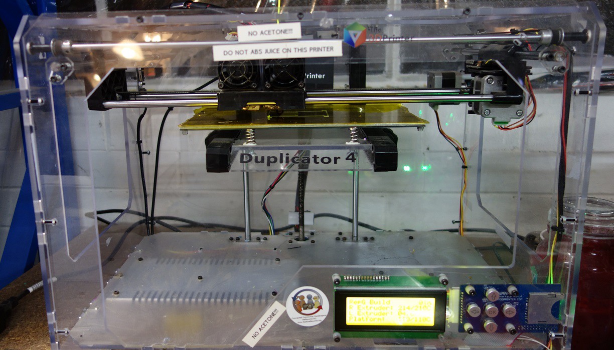
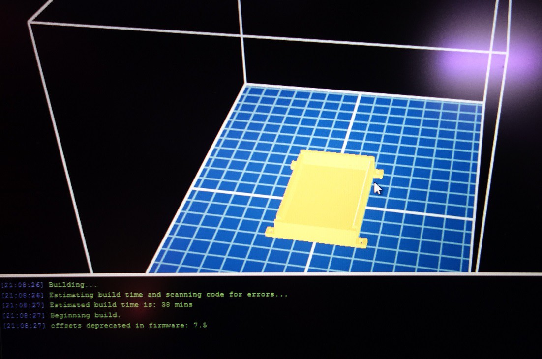
Above is the printer I have been using, located at the Melbourne Hacker space. Below is it doing its magic.
Reprinted the bottom as well as the top, now with different filament colour.
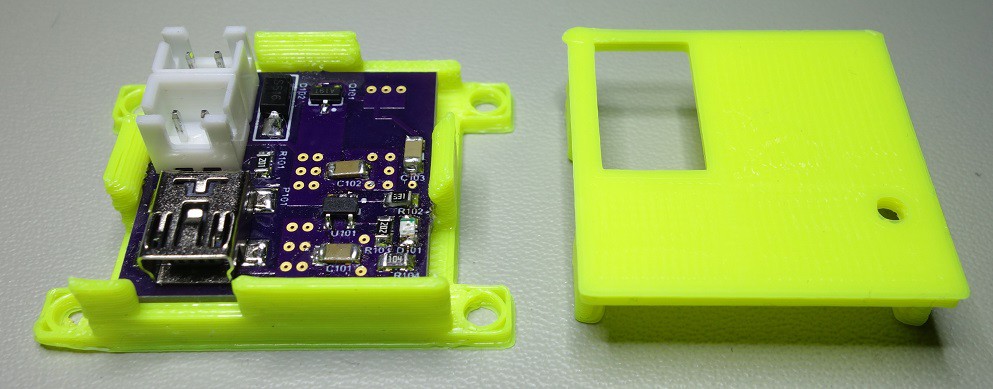
Another view, outlining the tabs on the top part.
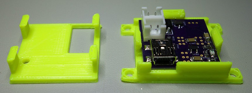
Below is when it parts clips into together.
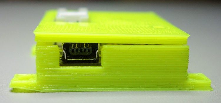
This is the view from the side.
With the front view you can see the USB connecter was taller then anticipated, however, the parts were still able to clip into each other.
I have also printed a bottom case for the LiPo battery, which was a snug fit for the battery.
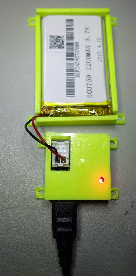
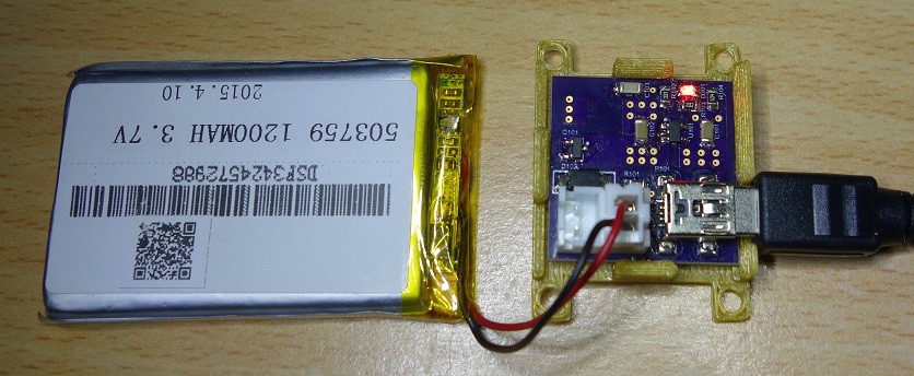
The red LED is only on when a battery is present and the battery is charging, otherwise its off.
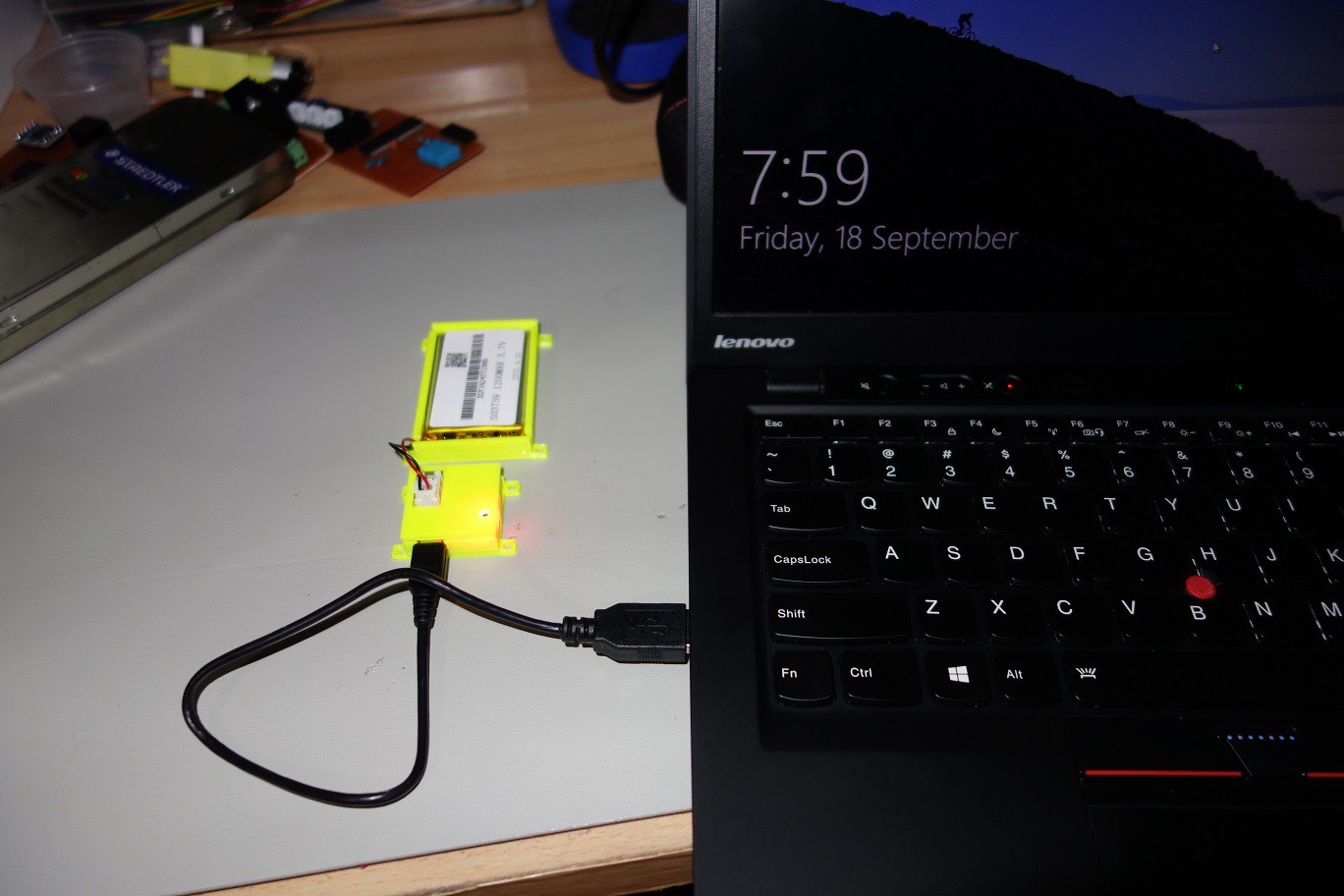
Test of confidence, by powering from my computer's USB port. I have been using a cheap mobile phone chargers from this.
-
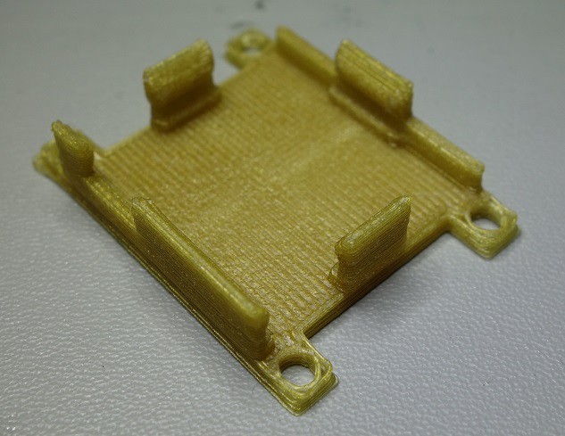
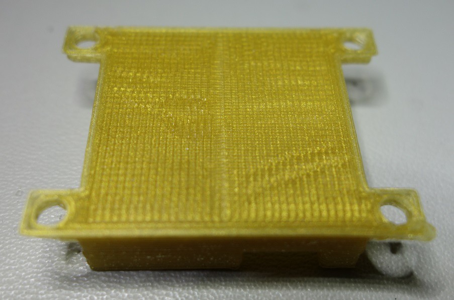
3D Bottom Case
09/15/2015 at 09:01 • 0 commentsI begin 3D printing the bottom part of the case and below is my third attempt print.
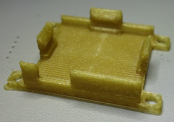
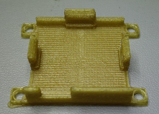
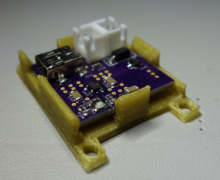
The idea is the PCB should clip into the notches shown below.
Another angle of the bottom case.
Yet another angle of the part.
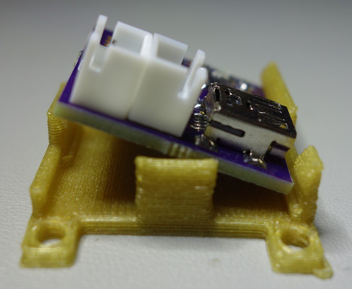
Fitting in the assembled PCB.
Another different angle of fitting the PCB.
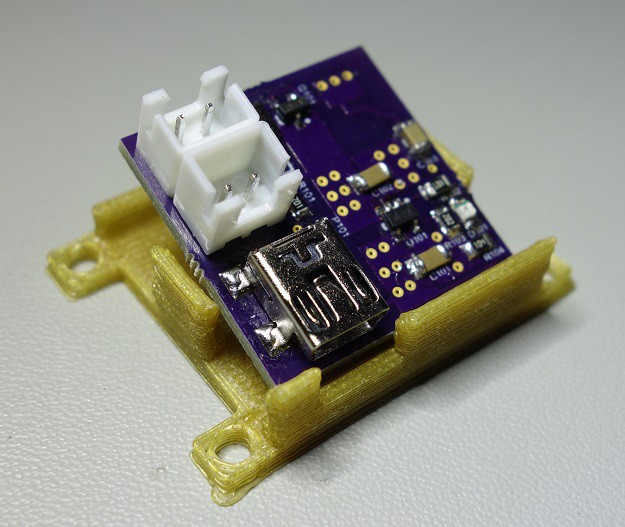
Below is when the it completely clipped in.
Notice that USB connector is too recessed and might require moving the connector more outwards.
The connector is still pluggable and charges without issue.
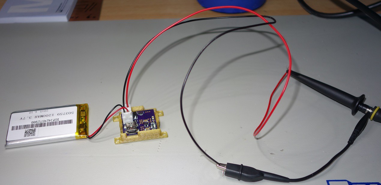
Now testing output ripple and report back.
Lastly, noticed that the PCB is able to move around a bit and will need to look into improving the fit.
-
Ordering PCBs
09/06/2015 at 18:19 • 0 commentsBefore ordering the PCBSs, I first need to generate the Gerber files from my EDA program and ensure my design met the design rules of the fab house. See https://oshpark.com/guidelines for more information.
For this section, I decide to cover how to generate the Gerber files step by step and finally ordering the PCB from OSH Park.
I use Altium Designer as my EDA program and WinRAR to make the WinZip file required later on, therefore your mileage may vary.
I would like to thank John (https://hackaday.io/Johnny) for helping with figuring out the steps and I hope this helpful for anyone thinking of making PCBs.
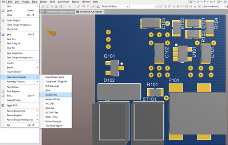
The first step is opening the PCB document and File > Fabrication Outputs > Gerber Files.
![]()
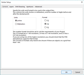
You should be presented with following window and you need to select Inches and 2:4 format.
![]()
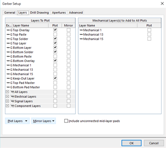
Go to the layers tab and the select the required layers.
![]()
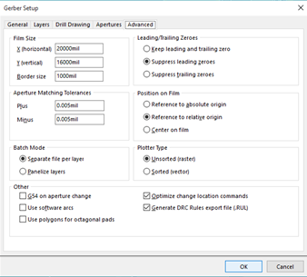
Check final tab and should have the following setting. Click "OK" and the EDA will generate the CAM file.
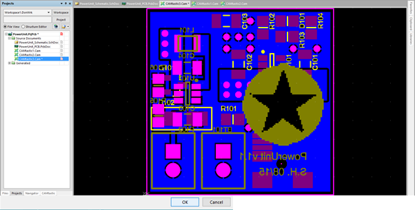
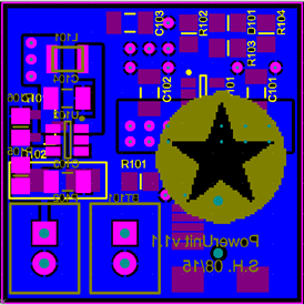
![]() The CAM file should be in view, however, there is no holes present. Therefore we need to generate the drill files.
The CAM file should be in view, however, there is no holes present. Therefore we need to generate the drill files.![]()
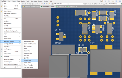
Go back to the PCB document and select File > Fabrication Outputs > NC Drill Files.
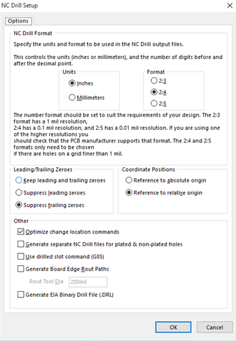
![]() Ensure the setting is the same as follows and then click "OK".
Ensure the setting is the same as follows and then click "OK".![]() Once drill files are generated, we need to import those files into the CAM documents. First open the CAM document and select File > Import > Drill.
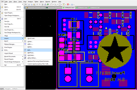
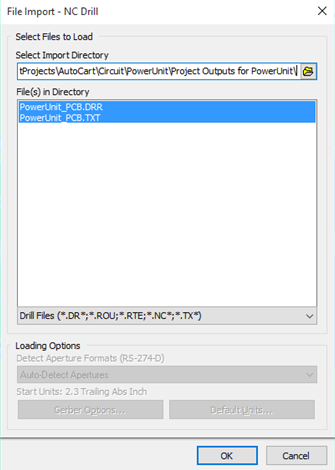
Once drill files are generated, we need to import those files into the CAM documents. First open the CAM document and select File > Import > Drill.![]() We need to navigate to the Project Outputs folder in the presented window and ensure we select the following files and click "OK".
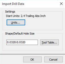
We need to navigate to the Project Outputs folder in the presented window and ensure we select the following files and click "OK".![]() For the next window, simply click "OK".
For the next window, simply click "OK".![]() Now Altium should show a status report. Just open the CAM document again and now there should drill holes. Ensure that holes are in the correct locations.
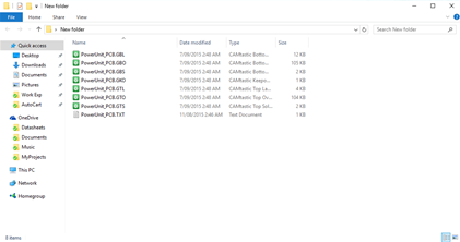
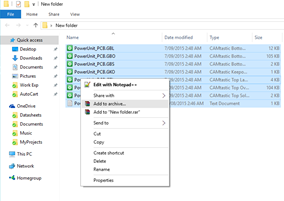
Now Altium should show a status report. Just open the CAM document again and now there should drill holes. Ensure that holes are in the correct locations.![]() Now navigate to Project Output folder and copy over the following files. Double check that file extensions are same as the required extensions covered in the Fab house design guidelines.
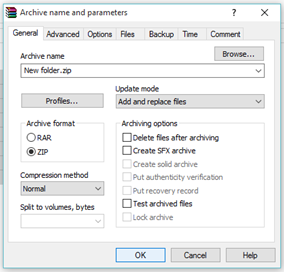
Now navigate to Project Output folder and copy over the following files. Double check that file extensions are same as the required extensions covered in the Fab house design guidelines.![]() The files now need to be in a single zip file and that will be the file we send to the Fab house.
The files now need to be in a single zip file and that will be the file we send to the Fab house.![]() Ensure its in a WinZip archive format, I have not tested archiving the files in a WinRAR format as the Fab house specifics a WinZip.
Ensure its in a WinZip archive format, I have not tested archiving the files in a WinRAR format as the Fab house specifics a WinZip.![]() Now you can import that WinZip file into OSH Park.
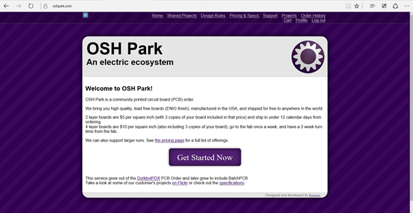
Now you can import that WinZip file into OSH Park.![]() Navigate to https://oshpark.com/ and click "Get Started Now" to view the next window.
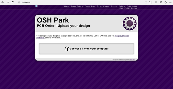
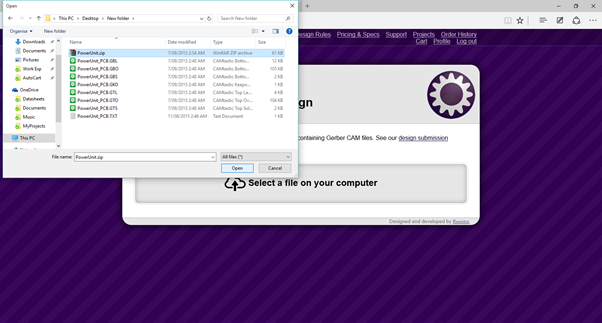
Navigate to https://oshpark.com/ and click "Get Started Now" to view the next window.![]() Click "Select a file on your computer" and select the WinZip file from before.
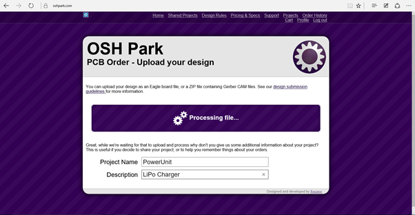
Click "Select a file on your computer" and select the WinZip file from before.![]() Once you selected the WinZip file, fill in the details while the site is processing the file.
Once you selected the WinZip file, fill in the details while the site is processing the file.![]() If there are no errors, you should be present with the following windows.
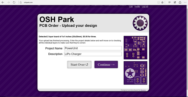
If there are no errors, you should be present with the following windows.![]() Click "Continue".
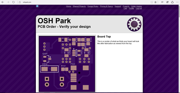
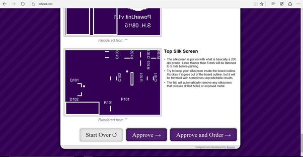
Click "Continue".![]() Check the presented images to ensure all layers are correct.
Check the presented images to ensure all layers are correct.![]() Once happy with PCB, go to the bottom of the page to approve and order the PCBs.
Once happy with PCB, go to the bottom of the page to approve and order the PCBs.Only steps left is registering for a OSH Park account, adding details and paying for the order.
From order the PCBs to them arriving in Melbourne, Australia took just about three weeks.
One important mention is the need to ensure you have a board outline within the Keep-Out layer. If there are no board outline, we will get an error in OSH Park. This was not a issue when importing the PCB without the board outline Seeed Studio, however, I have not order a PCB from them yet.
I will be sharing my Gerber files once I figure out the best place to host them.
-
Final PCB design
09/06/2015 at 16:46 • 0 commentsThe idea was the once I finalized my design, I would order the PCBs from OSH Park.
Given the size was 1 inch by 1 inch, it was the most cost effective as I was $5 shipped to Australia.
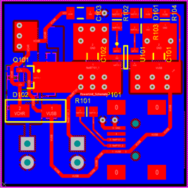
![]() Top layer of my PCB, I have hid the top overlay.
Top layer of my PCB, I have hid the top overlay.![]()
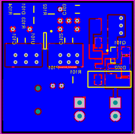
Bottom layer of the PCB and likewise I have hid the bottom overlay.
![]()
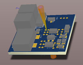
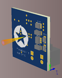
Top 3D model view.
![]()
Bottom view of the 3D model.
-
Schematic design
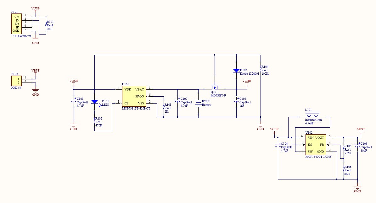
09/02/2015 at 02:01 • 4 commentsThis was my schematic design of my charger + boost converter. The wiring for the two chips were covered well in their respective datasheet and had a suggested PCB layout as well.
![]() I was informed by K.C. Lee of the incorrect units of the resistors in my boost converter part. I have changed it to the new correct units and the revised schematic is below.
I was informed by K.C. Lee of the incorrect units of the resistors in my boost converter part. I have changed it to the new correct units and the revised schematic is below.![]()
 Suleyman Hashi
 Another view, outlining the tabs on the top part.
 Below is when it parts clips into together.
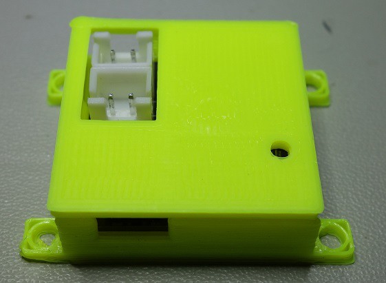
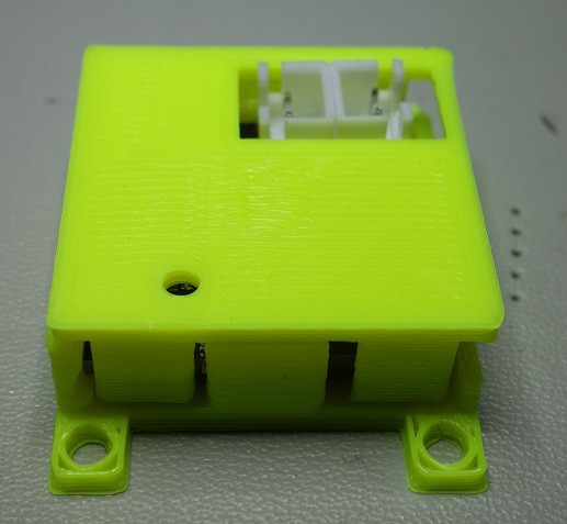
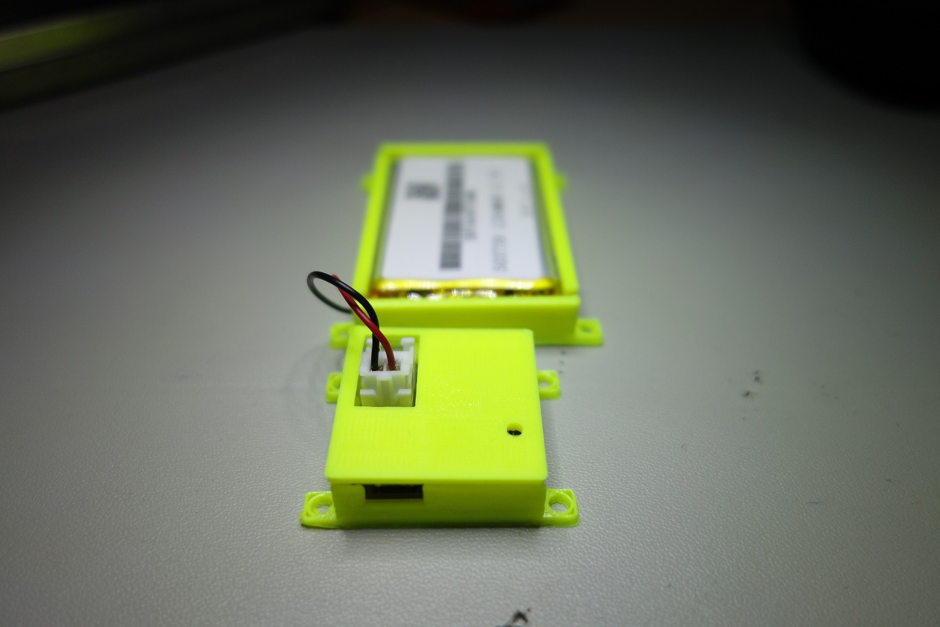 The red LED is only on when a battery is present and the battery is charging, otherwise its off.
 Test of confidence, by powering from my computer's USB port. I have been using a cheap mobile phone chargers from this.
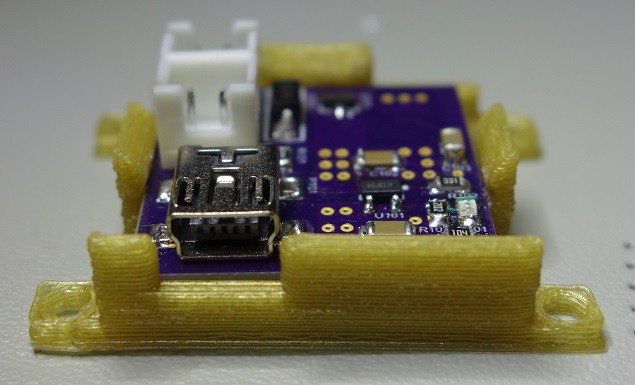 Notice that USB connector is too recessed and might require moving the connector more outwards.
 The CAM file should be in view, however, there is no holes present. Therefore we need to generate the drill files.
 Top layer of my PCB, I have hid the top overlay.
 I was informed by