Today, can we still design cool stuff without a FPGA or microcontroller ?
Have a look at the little brother of this project : #YGRECmos !
I have been teased by many BMOW like MyCPU80, the #The T-1: A discrete 8-bit Stack Computer, the #Fourbit, the #AYTABTU - Discrete Computer... (to name only a few, the list grew so much I had the create #Hackaday TTLers)
I felt the need to restart this project of a DIP-based minicomputer, like I imagined when I started the YASEP project more than a decade ago. Except that now, power consumption and parts price should be kept low, all the parts should also be available in SMD package because the final version will be on flexible PCB !
This is so ambitious that I must start and spin-off several sub-projects like #PICTIL, #Low-resolution scanner for cheap data input or #DYPLED ...
General architecture
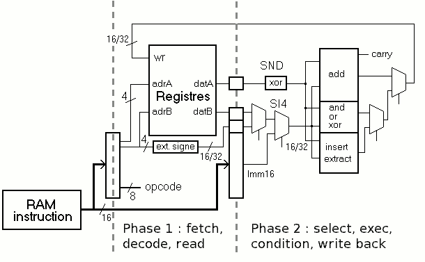
The architecture is adapted from the #microYasep where instructions take two cycles. It has a characteristic "2 reads - 1 write" heterogenous register bank that is accessed once or twice for each instruction depending on its length.
The following picture shows the datapath of the microYASEP and its two phases. The general organisation is preserved but the design will be split in a totally different way.
There are 3 memory banks, each 32K*16 bits and dual ported :
- Instruction space
- Data bank 1 (usually: working memory)
- Data bank 2 (usually: stack and stack frame)
(a 3rd address bus is MUXed for convenient debugging)
A custom, internal bus is being defined, which connects all the boards :
- user/control panel (read and write registers in hexa, connect to a host computer)
- Debug (trace, breakpoints, perf/events counters) [optional in the final version but life-saving during development and factory tests]
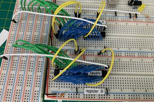
- register set (R2, R3, R4, R5) (or should I say "counter set" ?)
- Memory bank 1 (A2/D2, A3/D3)
- Memory bank 2 (A4/D4, A5/D5)
- Program memory (PC, R1, as well as A1/D1 to read/write instructions)
- ALU (also gives access to the SR and I/O spaces)
- Control/decode/sequence logic
- Memory editor / instruction assembler (optional too)
- Framebuffer (LCD and/or VGA output)
- Sound in&out, joystick
- User circuits, breadboard zone (so you can add your own devices)
- Result (DST="destination") : 16 data bits, 4 address bits, 1 strobe signal => writes data to one of the 16 registers
- SND and SI4 : 16 data bits, 4 address bits => read the 16 registers
- Current Instruction word (16 bits)
- Current PC
- Auxiliary address bus (for debugging/memory edition)
However it is not meant for I/Os, only for architectural exploration and debug. The ALU has the logic that deals with instruction operands and format so SR and IO are connected there.
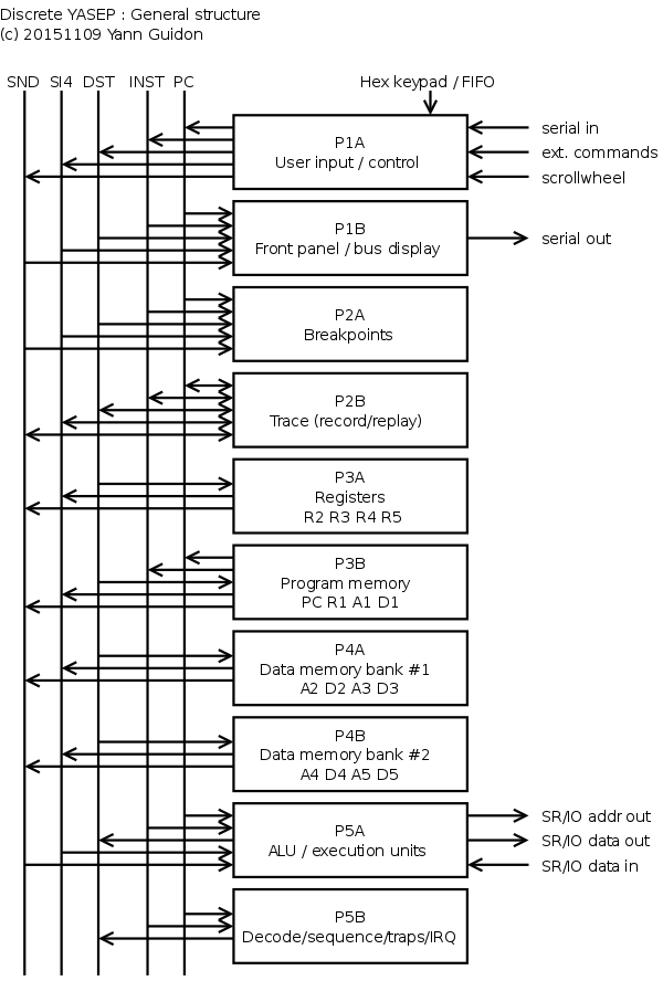
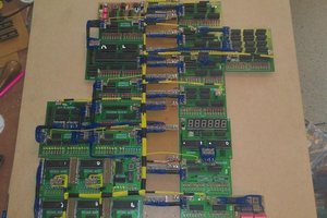
Each board's size is "double Europe" (160×200mm) and is paired with a neighbour (hence the A and B suffix). Pairs of boards are connected to the others with through-board pins.
Most buses use "3-state" logic to multiplex data, which is not ideal but saves some complexity.
Power supply
Hopefully the final version can be powered from a USB port so the power envelope would be 5W. An additional power input might be necessary though. The prototype has some DIP chips that need 5V but the whole system will be 3.3V in the final version. DC/DC converters are used and a mix of HC, HCT and LVC parts translate logic levels.
Logs:
1. First page and first roadblock
2. Board 1 : the user interface
3. Board 2 : Register set
4. Board 1 : the user interface (second take)
5. Design of the input FIFO
6. Clock generation circuit
7. The progress so far
8. Keypad musing
9. Emulation
10. Command and control as ASCII bytes
11. Asynchronous serial reception
12. User Interface Board overview
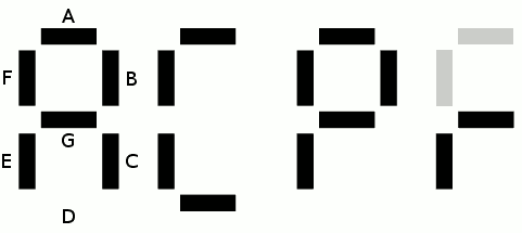
13. "Redneck" disintegrated 7 segments decoder
14. Keyboard proof of concept
15. Pulls!
16. Dear SN74HC688
17. Single stepping and scroll wheels
18. Sunday bug mouse (Sun debug mouse)
19. Parts, parts, parts...
20. Even better hardware debugging
21. Random Available Memories
22. DILosaure rising
23. A better...
 Yann Guidon / YGDES
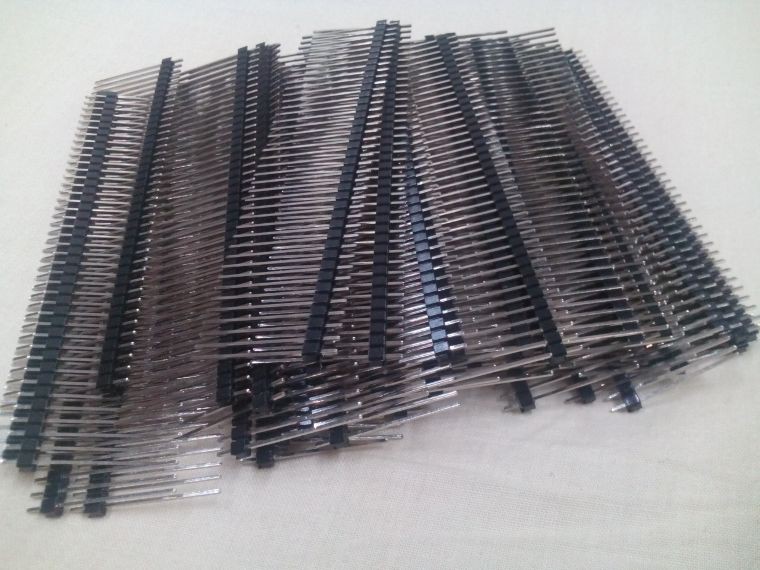
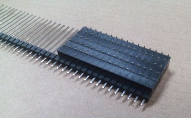
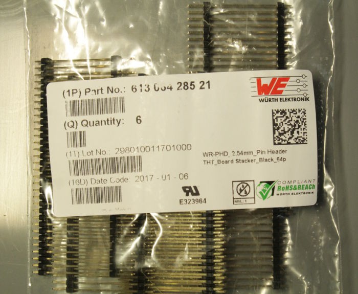
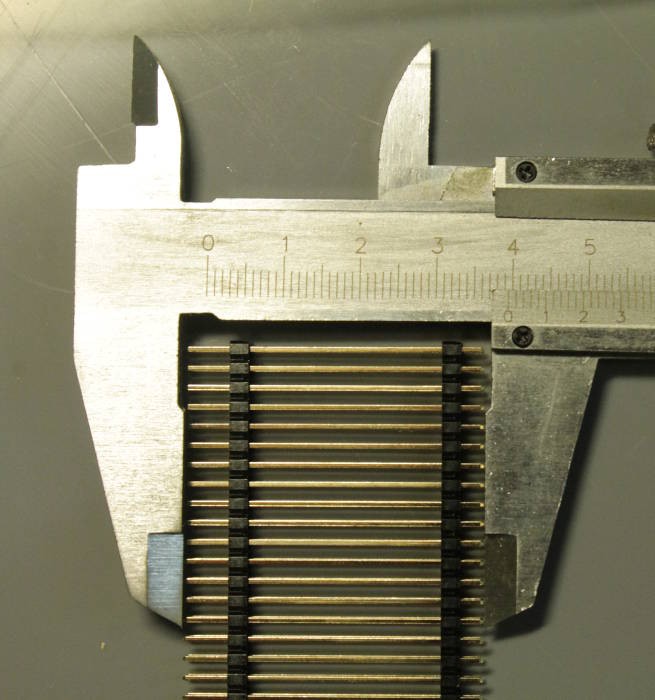
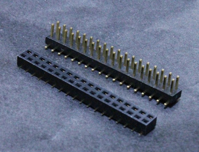
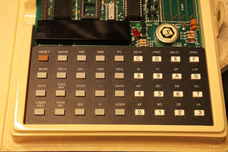
 And some days ago, I received this :
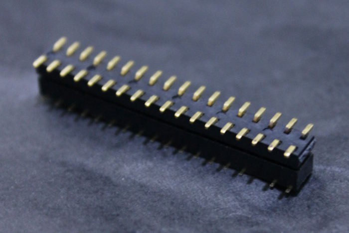
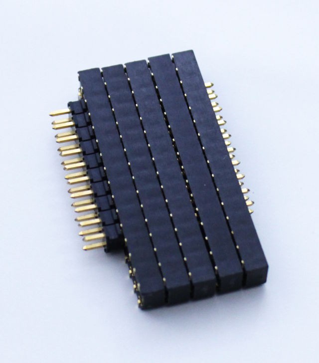
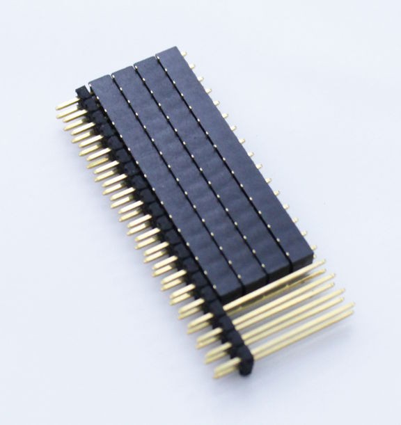
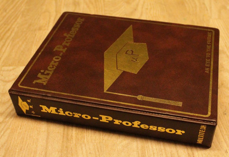
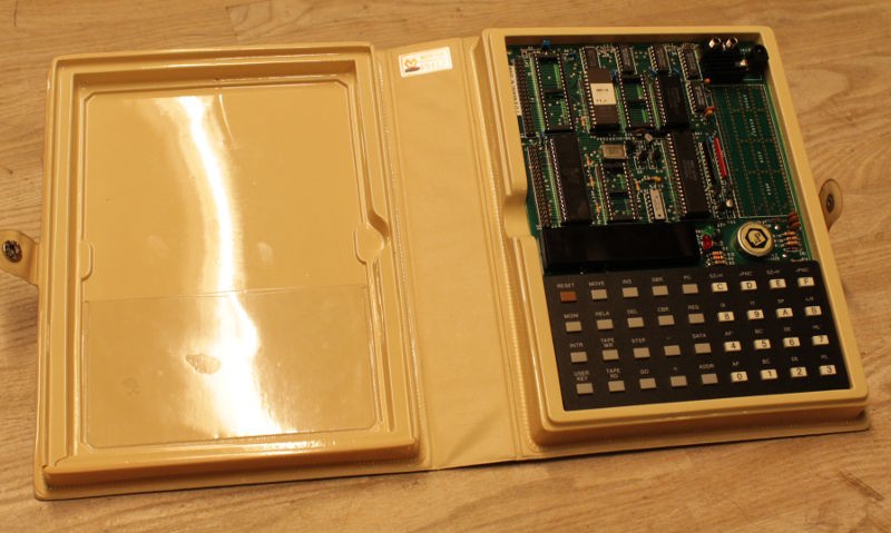
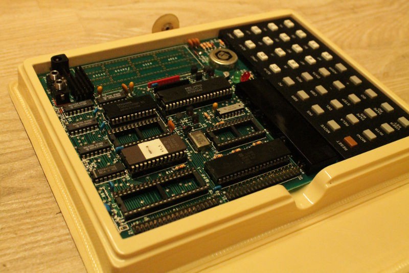
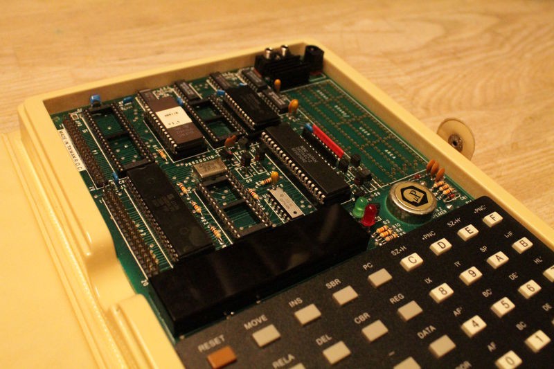



 matseng
 Charlie Smith
 Brandon Reinhart
I'd love to see a link to the actual instruction set (the picture on the main web site is very limited... e.g. what are the condition codes?) and the core block diagram (there is a very fuzzy picture in your blog of it which I can't read) and there is talk of a web simulator, but I can't find that either.