-
Prior art
05/21/2017 at 21:15 • 12 commentsI've been hinted at this 43 years old project from Elektor:
https://archive.org/stream/Computer74/computer-74
It's exciting that this idea has been in the air for so long, and yet we don't see it widely spread...
-
Got the backbones too
10/21/2016 at 12:17 • 0 commentsAfter Progress, at last !, I went looking for "ribs" (or "fishbones") or the backbone of the system.
![]()
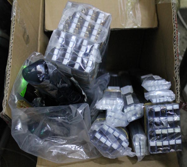
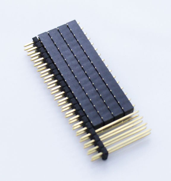
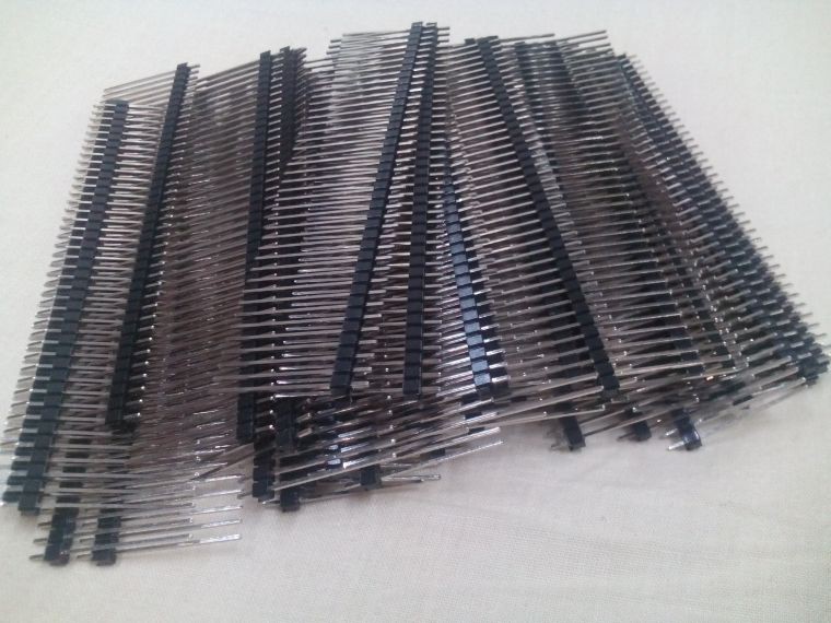
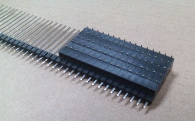
I found extra-long pins on eBay in sufficient quantities, smaller than what I have in stock but still enough to stack 5 pages. It should be enough for the first implementations...
The main PCB could serve as P1A/P1B... or something else requiring a rigid/solid base, connectors etc. so that makes 6 pages.![]()
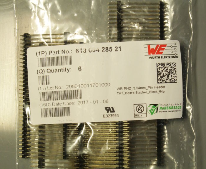
I received samples from Würth Elektronik !
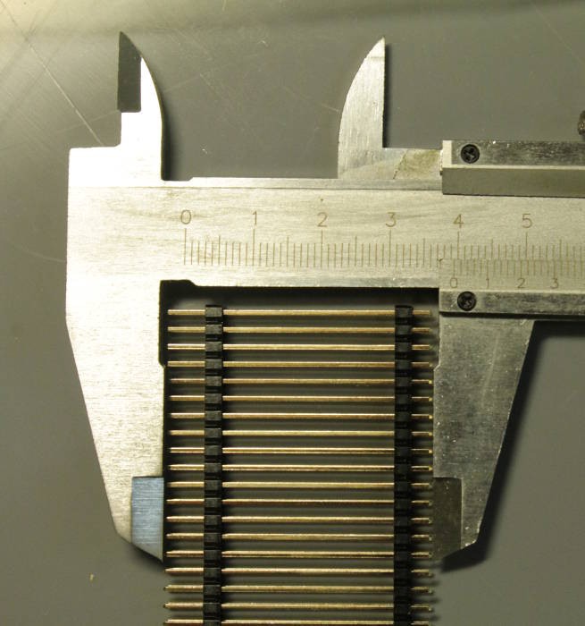
Thanks to the cool rep, we found a reference that is longer than the previous ones, almost 40mm (so the above picture is a reminder for the reference for a next order)
I might have also found very interesting prototype boards that can be slightly bent...
-
Give that man a cookie
05/08/2016 at 04:48 • 0 commentsIt all started in january 2016 with a suggestion to @Stefan Lochbrunner about a new #Breadboard Widgets module (see the comments).
He quickly created a nice board layout, which he uploaded to his git repository.
![]() And some days ago, I received this :
And some days ago, I received this :(I'll have to test them now)
Thank you so much, Stefan, I owe you one #DYPLED (once it's working) ;-)
That, the #PICTIL story and other personal experiences, confirm that German hackers are among the best ;-)
Someday I should make a similar breakout board for the Flash chips that I use in #DYPLED (see the yellow adapter board in Stack-based programming, which is nice but expensive and quite large)
-
Progress, at last !
05/03/2016 at 00:47 • 0 commentsA few things have kept this project from flying higher...
- work
- other projects (damn, 33 now ! am I bulimic ?)
- the multiplexing logic of P1A
- board-to-board SMD connectors (I don't have the matching connectors and they are pretty expensive but I need a significant quantity...)
The last problem seems to be solved, while cleaning up the workshop...
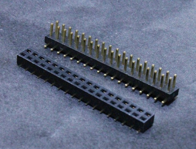
I found a decent supply of 2×16 SMT connectors. They are pretty low-density but the 2.54mm pitch is good anyway. Contrary to the expensive FX8-100P, with the 0.6mm pitch, it is possible to run traces through the pins so all the signals are used, instead of just one half.
I bought the matching male and female pairs on eBay, many years ago:
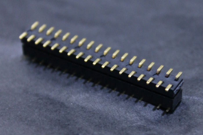
They are about 8mm high when connected:
8mm is a bit too high. However the receptacle alone is 3.7mm high. Add a Kapton foil and that's 4mm.The main board will have a lot of long pins to stick through all the pages. With 40mm pins, that's about 10 pages. I'll have to find longer pins but they might be found for wire-wrapping and such. That will be my next eBay search.
Until then I can prototype up to 5 pages with the pins I already have in stock.
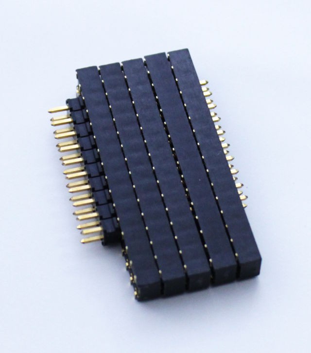
It's possible to cheat a bit by removing the black spacer after the pins are soldered, which makes 6 levels. I have other pins (more numerous) that can do 4 levels, eventually 5:
Now, the question is : how many of these 32-pins connectors does one page need ?
-
Displaying the register name
03/08/2016 at 23:07 • 0 commentsWith the experience gained from de #DYPLED subproject, I can easily design custom LED displays and the register names (on the P1B board) is a great application of the principles. The ingredients are the same : a large parallel Flash chip (1M×16), 4014 type LED (long, narrow and thin) for the segments, some multiplexing (one 2N7002 for the low-side driving of a group of LED), a binary counter to sequence all that (taken from the main clock divider) and one mode bit (to select between hex display and symbolic name).
P1B displays 3 buses: the result bus and the SI4 and SND source values. That's 3×4 bits. Add 2 or 3 bits for multiplexing, one mode bit and the address bus is under-utilized.
The 16 bits of output are used for 2 7-segments displays, leaving 2 unused bits. I'd like to "save" one more bit so the Flash directly drives the MOSFET's gate and saves a demux chip.
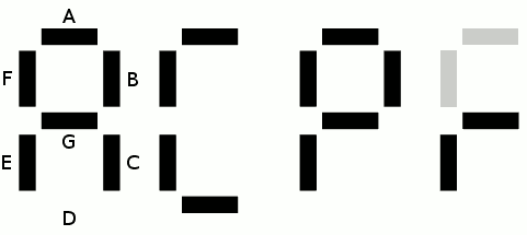
The rightmost digit displays the usual Hex numbers. The leftmost displays only 4 symbols, necessary to write the names Ax, Dx, Rx and PC. There should be a way to save a bit somewhere.
![]()
A first visual examination shows that the A and F segments are on at the same time so they can be wired in parallel. This saves the needed 3rd bit, without having to resort to external logic gates. Furthermore, the segment D is the inverse of the segment G but this would require an inverting gate.
In the end, decoding the register names uses only one Flash chip and 3 2N7002 :-)
-
Inspiration
01/29/2016 at 23:25 • 0 commentsI visited Labitat today
https://hackaday.io/hackerspace/4882-labitat
My host Christian was excited to show me a book-like box. And guess what ?
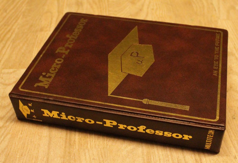
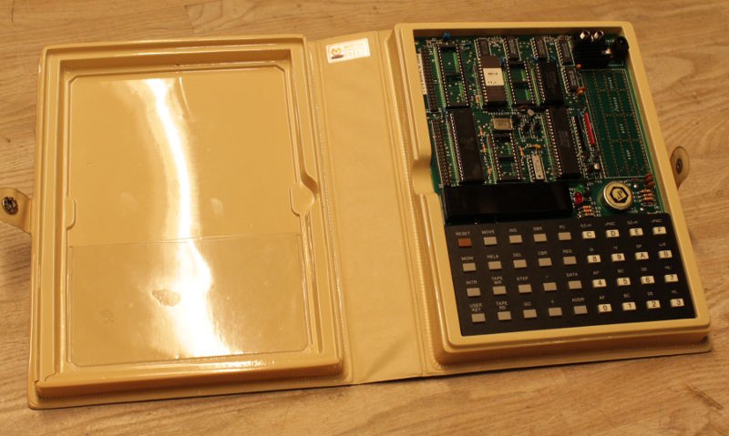
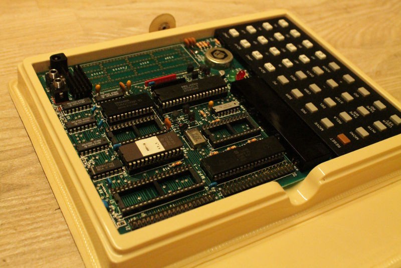
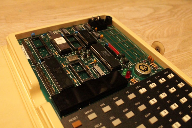
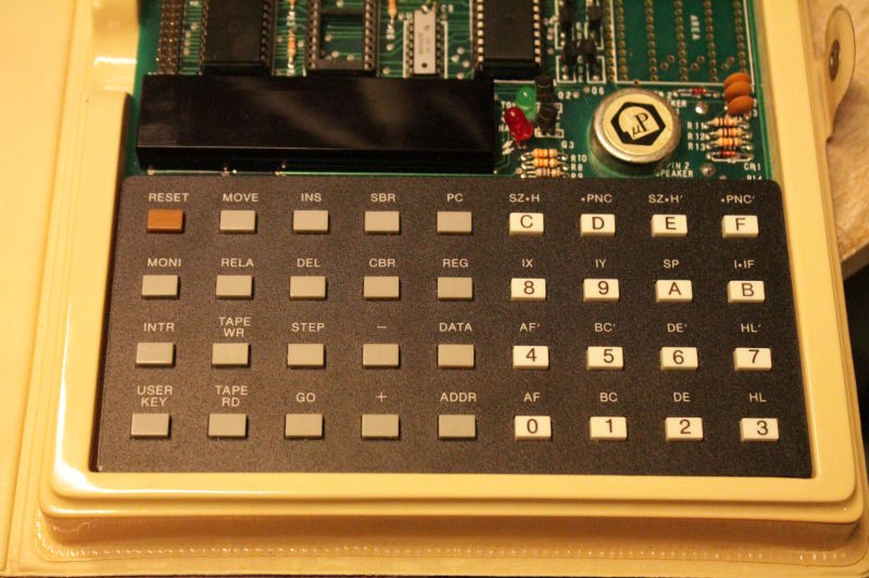
The MPF-1 is not a book, it's a computer. Which is more or less my intention with the Discrete YASEP...
Can you believe it's still manufactured and sold by Flite ?
I hope to add a MPF-1/88 to my collection, to remind me where the inspiration comes from and what to get "right", such as the programming interface :-)
The ability to assemble instructions without the need of manual assembly is precious. Typing hex codes is geeky but that's not an end in itself !I have noticed that the best development tools for a computer are also the tools that helped design it. With an open sourced design, both are the same and this makes the system even better :-)
-
How to verify actual timings and delays
01/15/2016 at 10:27 • 0 commentsAs the system becomes more complex, it's trickier to evaluate the actual propagation times of the signals. Datasheets can't be relied upon because of the variations between manufacturers and batches, the PCBs add capacitance and we never know anyway.
The only way to know is to measure. Inject signals at the input and measure the delays with the scope. But it is still pretty tricky because there are combinational and sequential logic stages, and not all paths have the same lengths, so a little signal could influence the propagation time of the whole rest. Think about the carry input of the ALU, or the control signals of SHL unit.
My solution is almost simple and it requires the fabrication of a special circuit. A huge LFSR made of a lot of of shift registers (74HC164 for example) and some XOR gates. For suitable LFSR polynoms, look no further than http://ygdes.com/GHDL/lfsr4/
The clock input can be selected from several oscillators, and the LFSR output are scrambled/shuffled to randomize a bit the generated bits. Each output of the examined circuit can be checked with a 'scope and jitter can be measured. Since the project is a 16-bits CPU, it's easy to cycle through the 64K input combinations and see "offending" (lagging) signals a few times per second, which is suitable for visual observation on a 'scope.
From these observations, subcycles from the main clock can be allocated for each unit. For example I'm curious about the REAL propagation time of a carry through a chain of 74HC193. I can only estimate the time with the datasheet but the real delay will influence how long the instruction time will take.
-
Clocking: the revenge
01/15/2016 at 10:03 • 0 commentsThere is a tie between the 24.576MHz and 18.432MHz source frequencies.
The higher the frequency, the better resolution for scheduling the sub-cycles of each instruction. Finer sub-step allow a faster execution.
24.576MHz allows 40.7ns steps, but it is not as handy as 18.432MHz to derive "useful" frequencies, for serial communication for example.
I have ample supplies of both frequencies. 24.576MHz is desired but how can I extract the 3.6864MHz that is used by the other circuits ?
24.576/3.6864 = 6.6666....
Actually it means : for every 20 cycles at 24.576MHz, there are 3 cycles at 3.6864.
You can substitute "transition" for "cycle" and it becomes pretty interesting, from a logic circuit perspective. A 74HC4017, a 74HC74 and some AND/OR gates will do the trick.
First, the 4017 will turn on one output every 10 cycles. One cycle is 2 transitions, right ? So one 4017 can work with 20 transitions. Each transition can be identified with a AND gate between the 4017 output and the clock signal (inverted if necessary).
One can evenly divide 20 by 3 with the intervals 7, 7 and 6. 3 AND gates are used to combine the 4017 outputs with the (inverted?) clock signal. The result is ORed and privides 3 pulses every 10 cycles.
The pulses clock a 74HC74 with the /Q output looped back to the D input, which makes a cleaner 3.6864MHz signal (with some jitter).
Did I mention that I love the 4017 ? :-)
This circuit is rather easy to build with discrete parts but I might have to use a CPLD or tiny FPGA for the sequencing logic, because the timing gets pretty critical. I wish I could reach 4MIPS, that's 6 sub-cycles @24MHz and only 4 @18MHz
Another interesting property of 24.576MHz is that it is a multiple of 2^16 (3×125×65536) and it's handier for power-of-two real-time scheduling (more on this later). OTOH 18.432MHz is "only" 16384×1125.
-
And now, the joysticks
01/13/2016 at 20:10 • 0 commentsAs I'm contemplating the sound input and output, I deal with ADC questions.
Since I'm able to digitize with 8-bits resolution at pretty high speed, I can also digitize at lower speed, position sensors for example. Several years ago, I played with those flat "thumb joysticks" made for the Sony PSP and they fit this project nicely.
So I'm adding this new feature to the specs : 2× X-Y analog thumb controllers with 8 bits resolution. The 4 values will be available in the Special Registers space. I'm not exactly sure yet how I'll deal with the button calibration (center value) but it's not as if nobody had to solve this before.
Looking more at the PSP, its screen is pretty cool too, 480×272px with 4.3" diagonal. That's not impressive but already good for $10. It would match my 1MB SSRAM budget, with a virtual framebuffer of 1024×512 for a nice scroll margin. No double buffering, though. The CPU is not fast enough to refresh everything in 20ms...
-
Board-to-board connection
01/10/2016 at 11:43 • 4 commentsThe final design will use the 100-pins Hirose FX8-100 connector. The PDF contains these pictures, to give you a rough idea :
![]()
The stacking height is only 3mm between two boards. Actually it will vary because the PCB wil bend ;) but pairs of PCB can be easily mated and moved up/down the stack as needed, that's important for modularity and repairs.
Why this connector in particular ? Well, in another life I was a ETX PC/COM format enthusiast and by chance I got a half-reel of FX8-100S-SV from eBay (this can happen why you buy a box with "various parts" that the seller has no idea what they are or why they are useful and can't list what they sell... you're never safe from a good surprise !)
Since this connector is used for the ETX COM format, availability is rather good. It has a lot of pins and the stacking height is about the thickness of SMD parts such as SOIC ICs.
Now let's see the little issues :
- The pin pitch is .6mm, it's not extremely thin, but thin enough to prevent wires from crossing from one end to the other with a standard 150µ etching rule. 150µ wire width and spacing is ok to run 2 wires in .6mm but there is no room left for the vias. The approach today is simple : use 2 contacts for one signal, so only 50 signals are available. This increases the number of required connectors... Maybe 3 or 4 are necessary.
- I only have S-type connectors (a few hundreds). The complementary P-type is harder to get. I'll be investigating in the coming months, to find decent prices (sub-$) in medium volume. It seems that compatible connectors are made by another manufacturer, that could be a clue...
When I have enough male/female pairs, I'll start designing a support board and generic flexible "pages" :-)
Discrete YASEP
a 16-bits YASEP computer (mostly) made of DIP/SOIC chips like in the 70s and 80s... with 2010's twists!
 Yann Guidon / YGDES
 And some days ago, I received this :
