Close
0%
0%

Discrete Binary to 7 Segment Display

Logic circuit to take a binary input and convert it to a 7 segment display

Similar projects worth following
Logic circuit to take a binary input and convert it to a 7 segment display using only discrete parts. (except the voltage regulator)

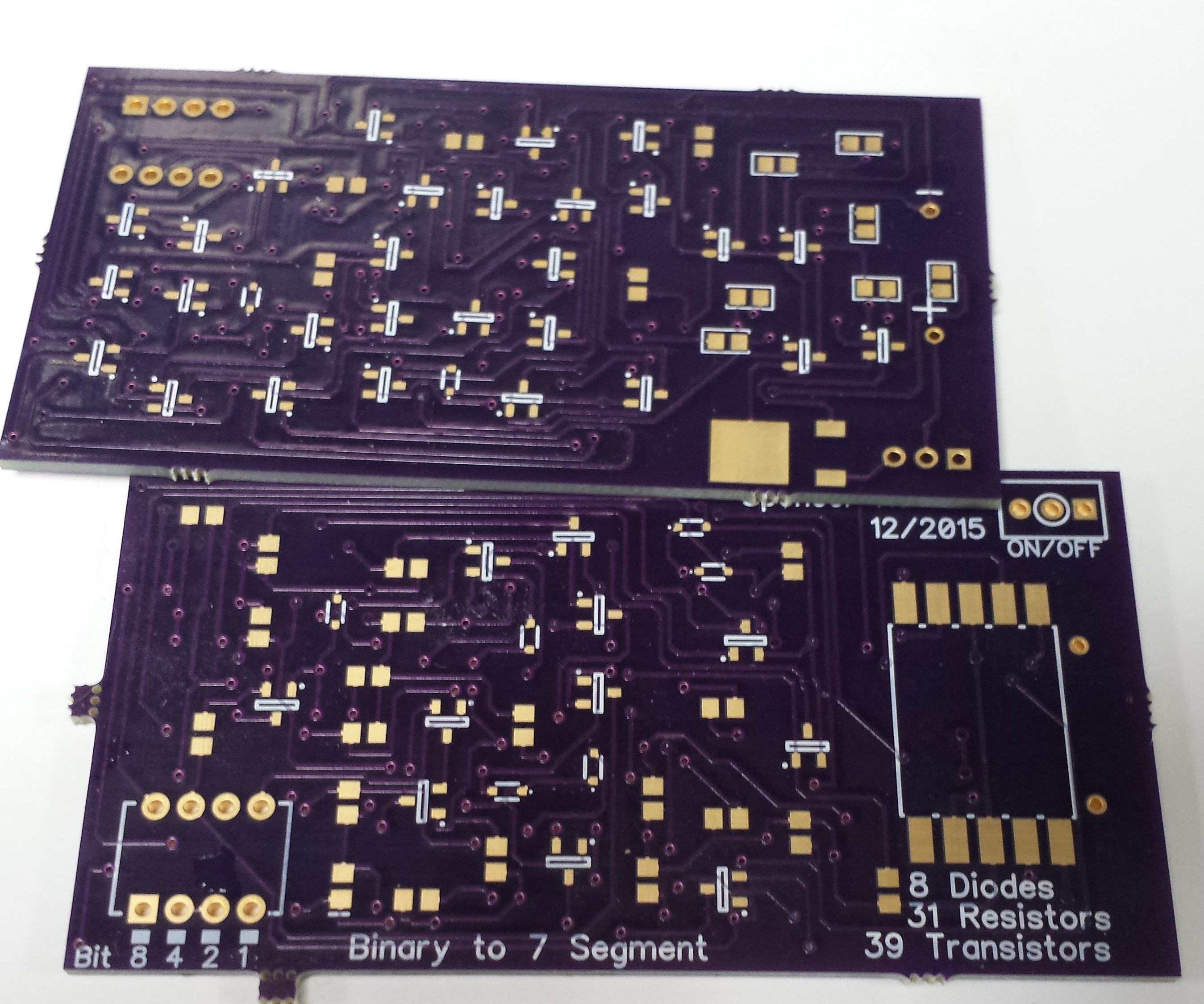
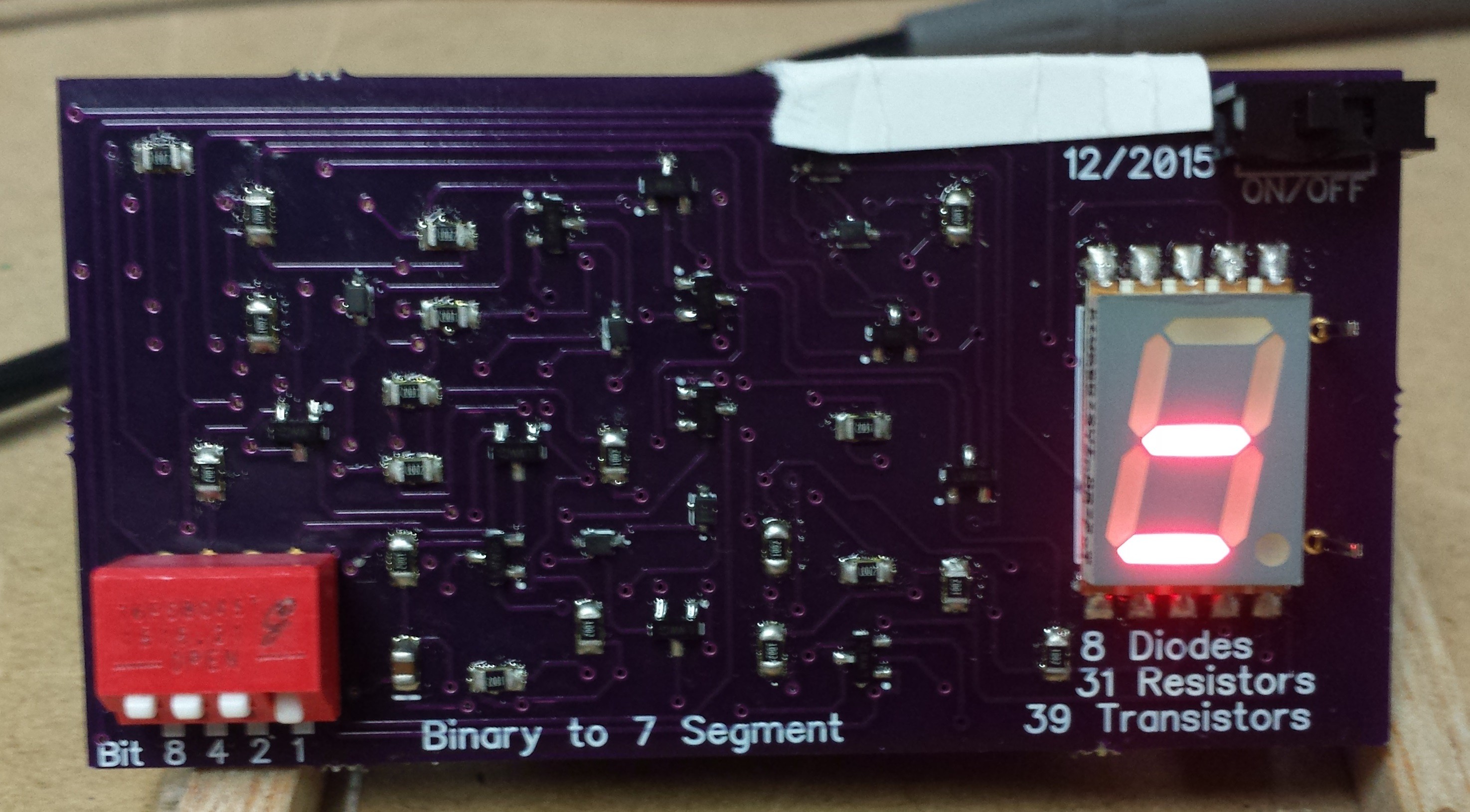
Building this was a real treat. I had long since reached the point where nearly every kit was far to simple and it was fun to get back into the action so to speak. V1 never worked and V2 worked with some modifications. I eneded up using 8 diodes, 31 resistors, and 39 Transistors.

All the relevant files are on git hub including an excel file listing part quantity with a digikey link. The PCB is about 5 square inches and they have been corrected and will now work with out modification. I bought mine from OSH park and it was about 30$ with shiping.

I used Diptrace for design however I proved a bit map image of the PCB for those who don't want to install it. The design comes in under 300 pins meaning it will work with the free version.

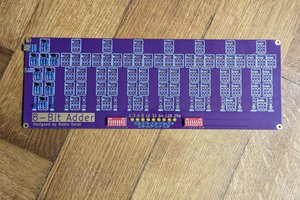
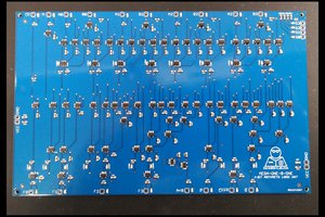
Bottom Layer.jpg

JPEG Image - 407.61 kB - 01/09/2016 at 23:08

Preview

Top Layer.jpg

JPEG Image - 362.96 kB - 01/09/2016 at 23:08

Preview

BCD Decoder V2 Inventory.xlsx

sheet - 12.91 kB - 01/09/2016 at 23:07

Download

BCD Decode v2 Final.dip

PCB File

dip - 278.48 kB - 01/09/2016 at 23:06

Download

BCD Decode v2 Final.dch

Schematic file

dch - 157.52 kB - 01/09/2016 at 23:06

Download

  • 8 × SMD diodes
  • 7 × 160 Resistor
  • 24 × 10K Resistor
  • 39 × NPN Mosfet 2N7002P

  • V2 max speed test and V3 considerations

    Spencer02/21/2016 at 19:34 0 comments

    Part of the purpose of this project was to act as a testing ground for future projects made out of discrete logic. With this in mind I was curious to find out the max effective speed of the decoder. To test this I attached my function gen to the 8th's position on the input of Bit 3 depending on how you describe it. This produced a path 5 gates long untill the path reached the buffer or F segment driver for the display. I attached my scope to the gate of this transistor and simply feed increasingly high speed signals into it.

    I observed some odd 50KHz oscillation on the positive portion of the signal when I drove it at 10Khz. It could be some sort of harmonic effect but the frequency of the noise seemed independent of the input frequency.


    At 50KHz the wave form gets a bit nasty and I deem this the max effective frequency. Currently I am using NAND gates pulled high with a 10K resistor. I'm going to experiment with lower values and see if the max effective speed changes.

    Now on to V3. I never planed to make a 3rd version but I might have a opportunity though my college to make a more educational version. I showed V2 to the professor who teaches the digital logic classes, a class I took and was able to apply to this project. She is interested in a though hole version that ideally will show the individual logic state of each gate. I thought of several ways to accomplish this but I settled on the most reliable option.


    I'm simply attaching an LED buffer to each gate. This double the part count but with a board this size, (I esitmate 15-30 inches) I want it to work the first time!

    On the left you have the old gate design and the right is the gate plus a buffer. For any one new these are simply 2N3904 BJT transistors.


  • V2 Assembly and fix

    Spencer01/09/2016 at 23:21 2 comments

    Getting boards is always a fun event. There's just some thing about holding a board that you designed. Being impatient I got started on it immediately.

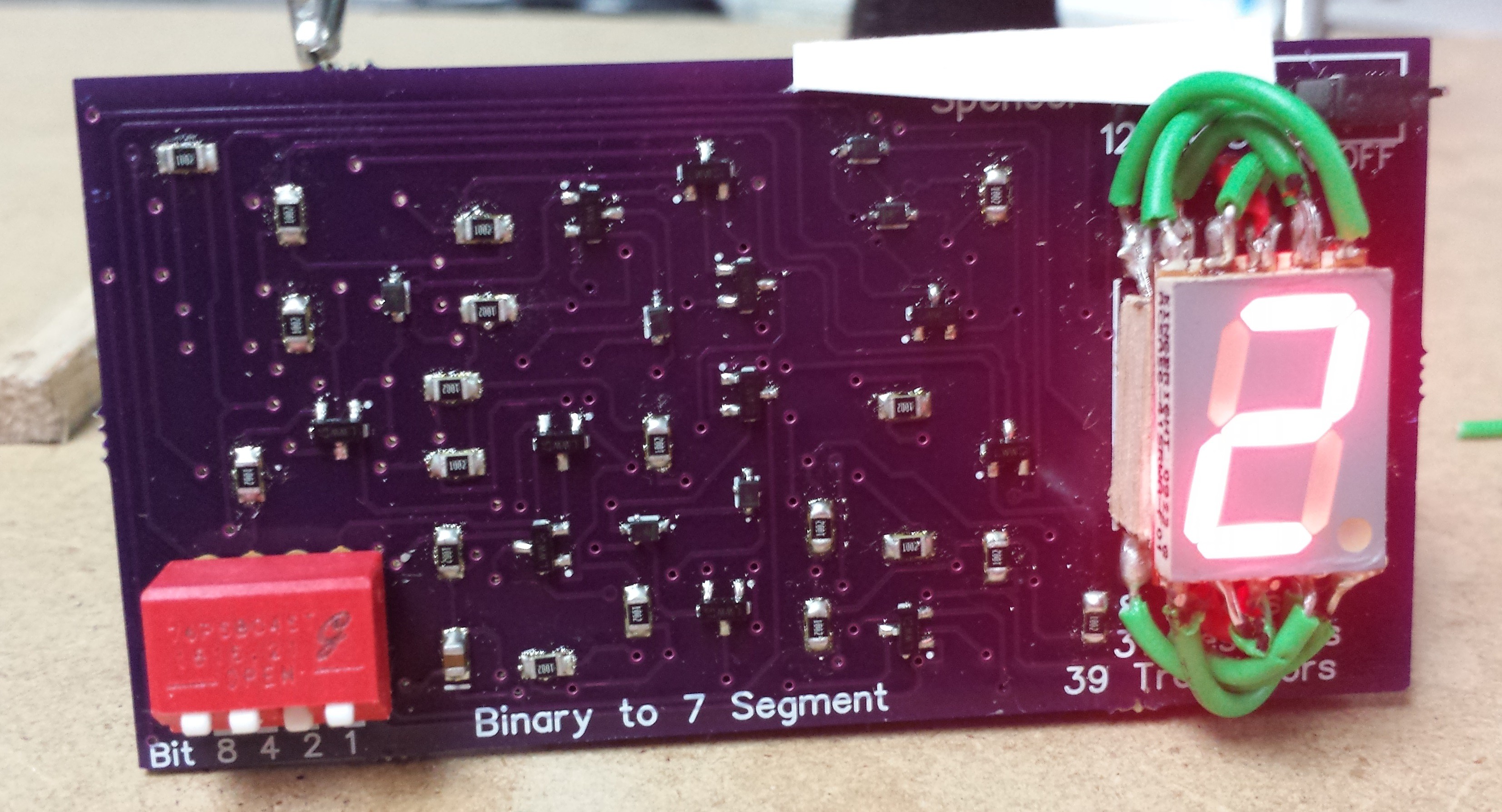
    My method of SMD work is sticking the parts down with solder paste (I have a syringe of it I use) and then using a hot air gun to melt it. It's tedious but so far I've always gotten good results with it. I saved the though hole parts for last and I was ready to see if it worked!


    It didn't...... My worst fear was an issue with the core logic circuits and it seems that seemed to be what the issue was. But then I noticed that the decimal point would light up in some positions. I never connected the DP to any thing, left it floating. I went back and reviewed the foot print. Sure enough I had reversed the foot print. Remember kids always triple check your work.

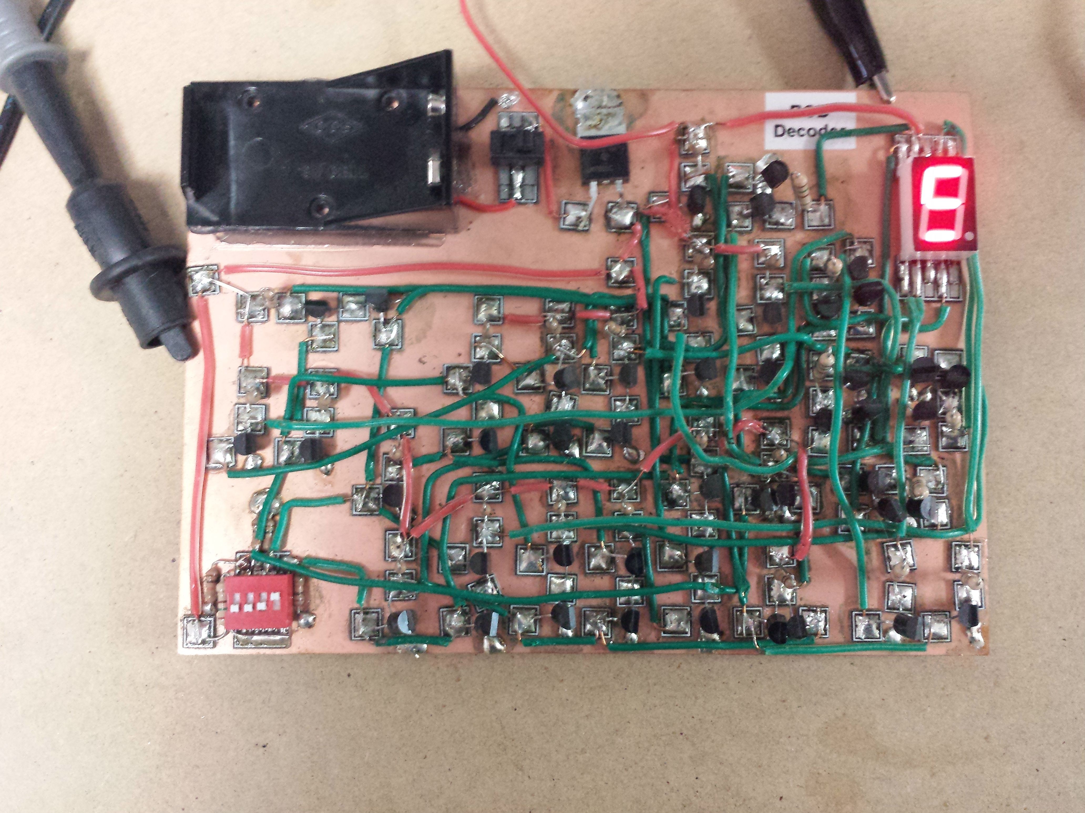
    This was fixable though and some tedious soldering later it LIVES!

    I did go back and fix the error. All the files on gihub are correct.

  • V2 and PCB design

    Spencer01/09/2016 at 23:00 0 comments

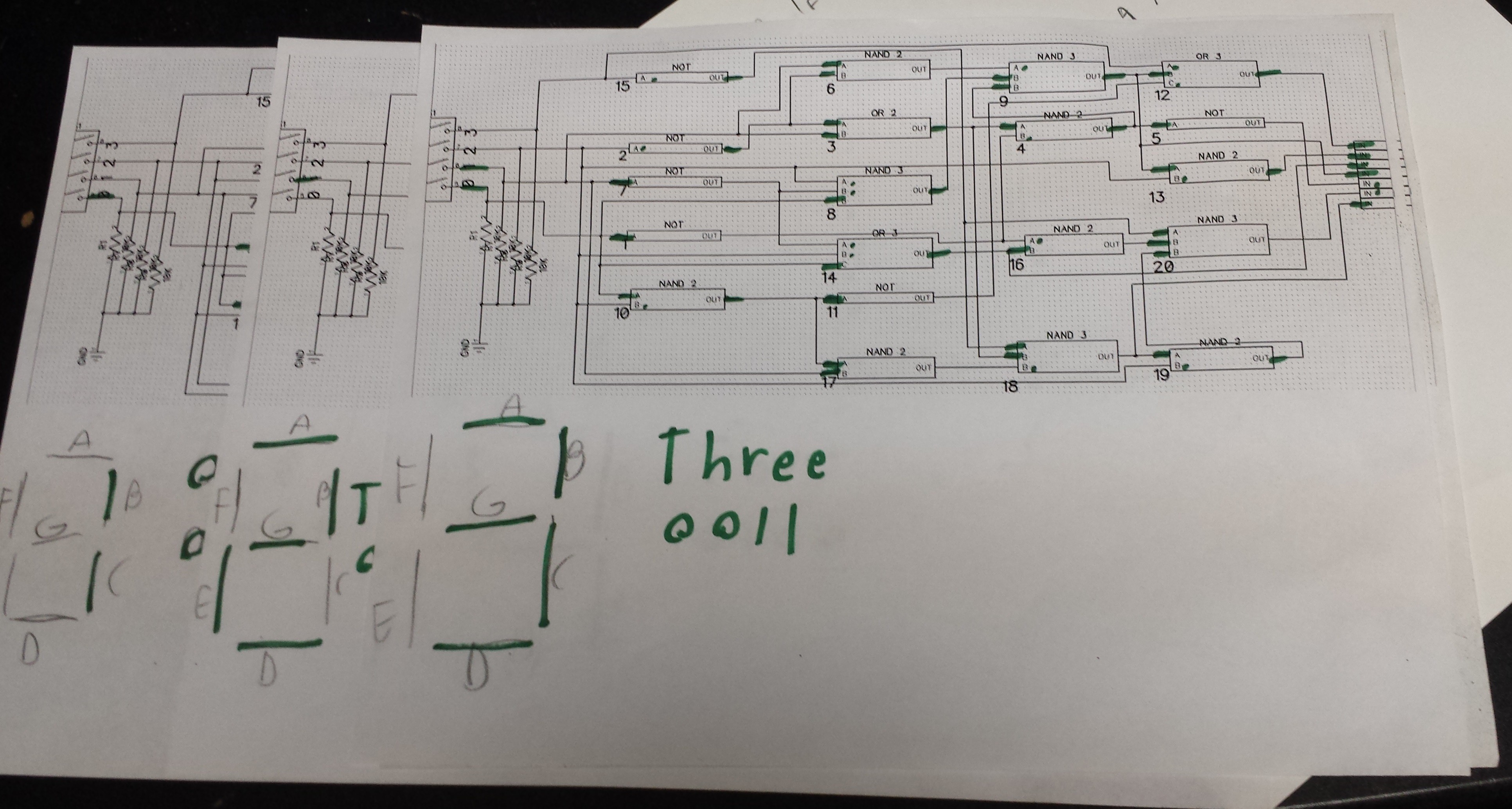
    When V1 failed it was nearly a year before tried again. I redid all the logic design portion as well making liberal use of logic Friday. The file is include in the Git hub. I then recreated the diagram in dip trace. However this time I had a new trick up my sleeve. I figured out how to use hierarchy blocks and was very generous in their usage. This made the schematic a lot cleaner witch for a project this large helps keep mistakes at a minimum.

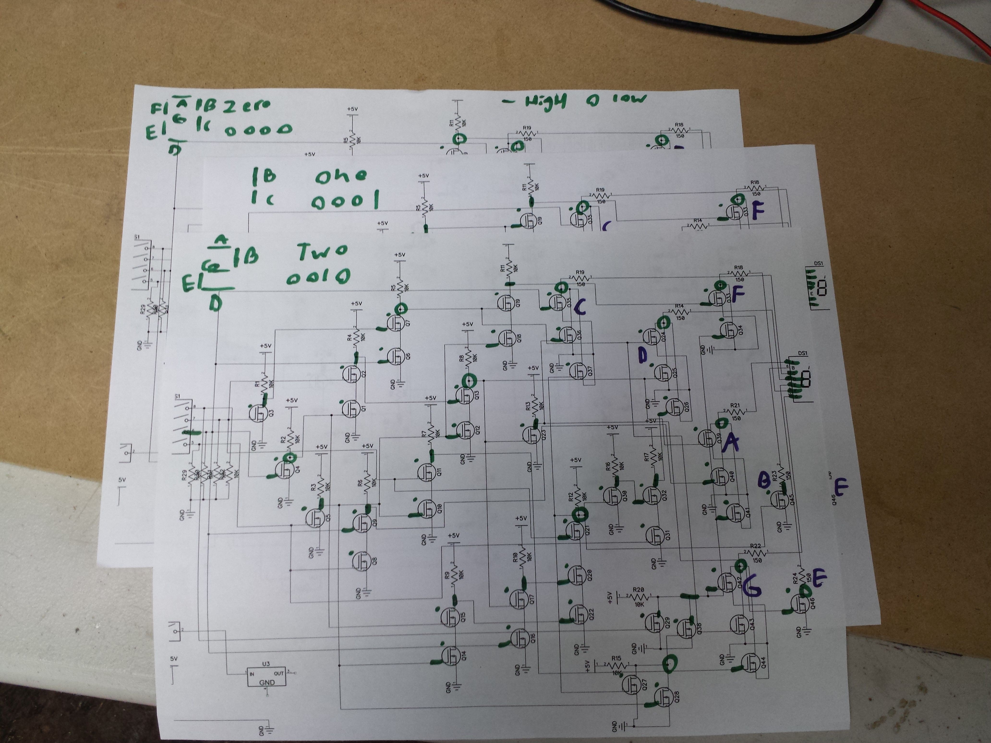
    This time I learned from my mistakes. I printed out the schematic and went though the first few numbers to make sure the out put was as expected.

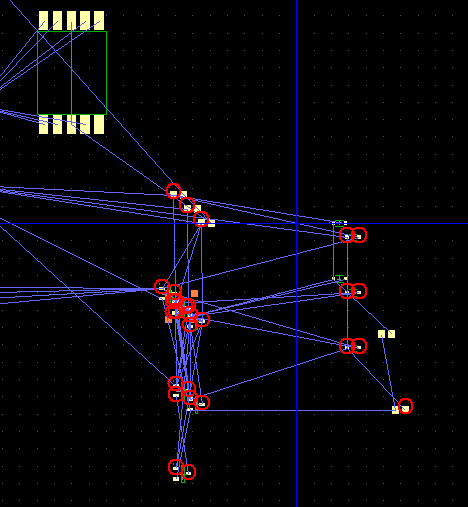
    With the knowledge the the core was sound I moved onto the actually PCB portion. I was hoping all the parts would be grouped close to their respective gates but I was massively disappointed. Turns out all the parts were directly on top of each other. As you can see in the picture below there are stacks of fets 2-5 fets deep.

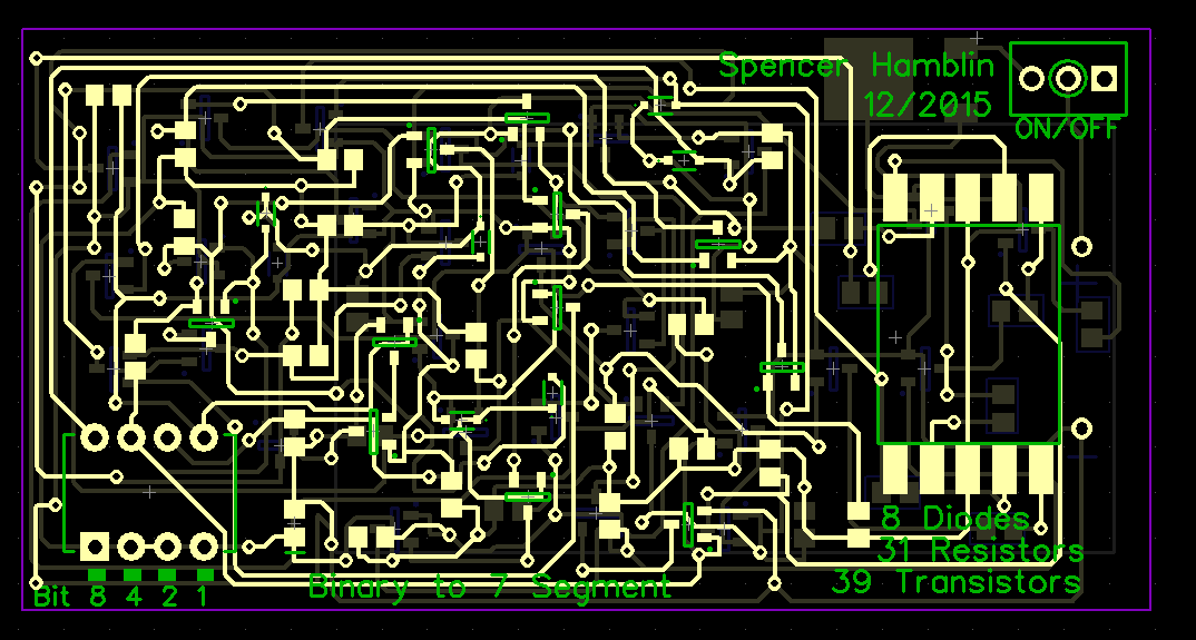
    I still took a shot at manually routing it but after getting frustrated I give in to the auto route. Initial results were pretty bad. I played around with it quite a bit but I managed to get it working reasonably well. The resulting PCB was ~5 square inches. I think it would be possible to get is smaller but that is getting close to the limit. The auto router did have to chew on it for a few minutes.


    The final result


  • Version 1 fail

    Spencer01/09/2016 at 21:43 5 comments

    V1 was a fail for multiple reasons. For some reason I decided to try to do the project Manhattan style. With the amount of connections and wires I had problems with connections. In addition to that I used cheap Fets from ebay of dubious reliability. What ultimately killed it however was the discovery that my schematic had multiple fundamental flaws.

    Reviewing the schematic

    I think this problem arose when I tried to convert it to using a common anode display. I got confused during this process and never discovered my mistake in time.


    V1 trying to display a 1

View all 4 project logs

Enjoy this project?

Share

Discussions

Yann Guidon / YGDES wrote 01/10/2016 at 07:15 point

It's funny how often this subject pops up. I'm not sure why you chose the logic way instead of the diode matrix way but I'm glad you tried :-)

  Are you sure? yes | no

matseng wrote 01/10/2016 at 12:44 point

But that would require a 4-to-16 bit decoder (a buttload of transistors and diodes) followed by about 80 diodes in the  matrix.  Not sure if that would end up with fewer parts...

  Are you sure? yes | no

Yann Guidon / YGDES wrote 01/10/2016 at 12:52 point

Damnit. You're not wrong.

  Are you sure? yes | no

Spencer wrote 01/11/2016 at 03:58 point

Funny enough some one on reddit had the same idea. You still have to use transistors in the BCD to decimal portion and ends up being only 14. However your now using 70 diodes. The circuit would be neater but might take up more space.

  Are you sure? yes | no

Yann Guidon / YGDES wrote 01/11/2016 at 04:32 point

at https://hackaday.io/project/8121-discrete-yasep/log/26997-redneck-disintegrated-7-segments-decoder I just need 33 diodes for the decoding matrix, using inverted logic. This decodes all 16 input codes, and 7 inverting FETs are required to amplify the output.
Yes the 4->16 decoder requires "some work" as well...
Did you consider using complementary FETs ? BSS85/BS250 ? This could save power at some places, partiularly when a signal is ON for only a fraction of the input codes.
I'm curious about the boolean equations you used, did you clone an existing circuit ? Does it support hexadecimal output as well ?

  Are you sure? yes | no

Spencer wrote 02/21/2016 at 20:02 point

The matrix uses 33 like you said plus the ones for binary to decimal ends up being 53 diodes and You still need to use 18 Fets. Going off this Binary to decimal converter. 

Maybe I'm missing some thing but that ends up at 71 semiconductor parts vs 47. 

As for complementary fets, I felt that they were too close to integrated circuits and I was after a purists solution. Just don't tell any one that the linear regulator is an IC :p.  And sadly it will not decode hexadecimal. I didn't really use any Boolean equations. I was lazy and just plugged the logic table into a program and had it do it for me. 

Sorry for taking such a long time to respond. I think I still need to figure out how to properly use Hack IO.

Also really cool project you've got! Your logs are really detailed and impreive! 

  Are you sure? yes | no

Yann Guidon / YGDES wrote 02/21/2016 at 20:49 point

Hi Spencer,

For BCD only I'm down to only 17 diodes now :-D

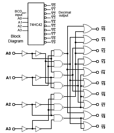
The HC42 seems to use a method similar to the one in my discrete clock : a layer of 2-input combination gates, and some predecoding of both halves of the "address".

Let's see: 7 NFET for LED driving, 17 diodes for decoding, 9*2=18 NFET for diriving the diode matrix (forget digit 8, it's all on).  What's left is the layer of AND2s. Input inverters : 4 FET.

Without ANDs, that's 46 semiconductors (why don't you also count the resistors ?) Add 2×7=14 for the AND2: 60 semiconductors.

The advantage is : easier to understand (no weird arbitrary logic). It's a layered circuit, each layer that can be examined individually and changed. Much easier to debug too ;-)

It looks like my discrete clock has increased my fluence with transistor logic :-D

  Are you sure? yes | no

Similar Projects

Does this project spark your interest?

Become a member to follow this project and never miss any updates