Michael O'Brien
-
Display Board
05/31/2014 at 07:02 • 0 commentsInitial design of the display board is done. Time to send it in to get fabricated. I'll look at the quote tomorrow morning. Outside rectangle is the glass boundary of the OLED screen. Inner is the viewing area.
![]()
The sides have 5 LEDs each: the two larger one are accent LEDs and there are much smaller warning lights above, between, and below those. Just realized that there is no way to have all lights remain off, as some may desire. I'll add in a 3-pin jumper to disable them before getting it fab'd.
In case you're wondering, I'm mounting the display upside down. I'll be using spare leads from through hole components as wire tie downs to secure the display at this time. The white strip is a slot where the cable will fit through with some clearance to prevent chaffing.
-
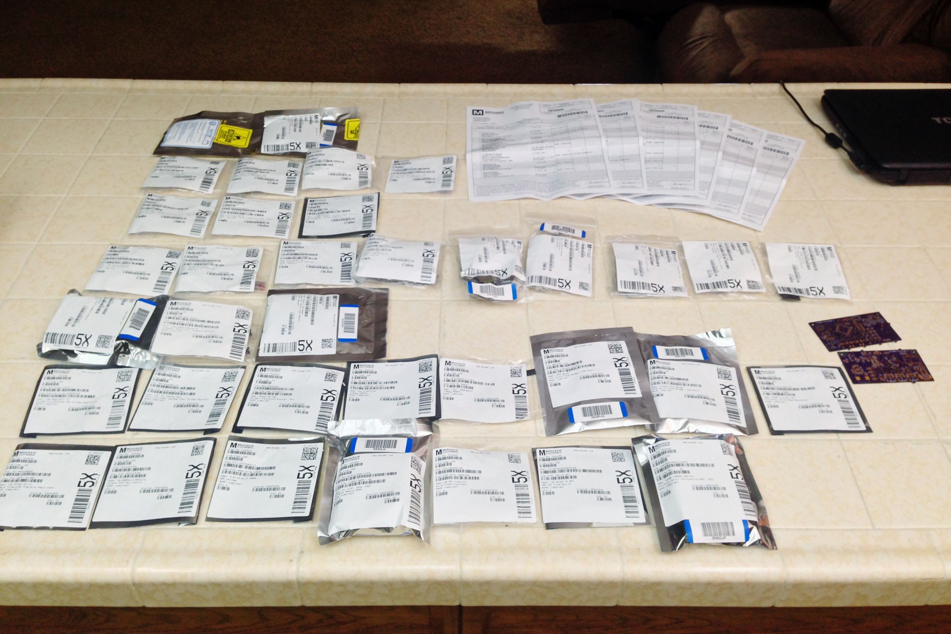
Batch 1 of Parts
05/30/2014 at 21:16 • 0 commentsChristmas in May!
![]()
-
Display PCB Layout
05/30/2014 at 02:33 • 0 commentsAfter much deliberation, I think I'll be settling on the following placement of the OLED display on the PCB:
![]()
The transistor pair on the left and right is vertically centered. Running the numbers places the graphical gauge face about 50 mil lower than vertical center. The outer circle has a diameter of 2.25".
Now that this is done, LED, et al., placement can now be finished up.
-
Sample Rate & Various Timing Considerations
05/29/2014 at 20:28 • 0 commentsThe biggest time waster for D-DAQ is writing out data to the displays. Now that I think I'm understanding how each of the separate processes are working together, I'm figuring out the timing for the software end to operate in worse case scenario, which is where I cannot utilize all 3 SPI channels simultaneously but instead have to serially access them. That being said, knowing how fast the design needs to sample it's 14 analog and 2 digital inputs is crucial.
The SPI bus will be running at 1:4 P-Bus, which is running 1:1 with SYSCLK. The ADC unit can convert up to 1 Msps, which is much greater than I need. I know some daq's run 20 Ksps or higher, but right now I will not be going that fast. How fast can I run it though without affecting display output?
SYSCLK is generated through a 4x multiplier of the external oscillator, which I'm setting at 16.368 MHz. This easily gives me the same frequency for my SPI bus. From what I've read, running the SPI bus at more than 50% duty cycle risks stalling the CPU. Now as I understand it the SPI bus operates "independently" of the CPU, i.e. it's not like bit banging where each bit requires CPU time, so once the SPIxBUF is written to or filled, a SPI transfer is initiated and the CPU continues on it's merry way. How long does it take to write to the buffer though?
Worse case scenario, I assume it takes an equal number of cycles as there are bits. This being said, lets run some numbers. 16.368 MHz (or bits), 50% (aka 1:2) DC, share that with 3 displays, and it takes 16 bits of data to represent 1 pixel. This leaves me with 682,000 pixel/sec (excluding any overhead, et al) per display at which I can write out per display. Sounds like plenty, but a 128x160 display has 20,480 pixels so this equates to ~33 fps; well below my desires 60 fps. Well, since I cannot spend my day writing to the displays and I have to sample the ADC as well, I have to figure out how much of the display I can update in one go before I have to attend to other things on the microcontroller.
20 Ksps is very respectable in my ignorant opinion, but again too high I feel. As I will probably be doing some light data smoothing, there is computational overhead that has to be factored in. So let's halve that to 10 Ksps. Those 682K pixels cannot just all be blindly written out but have to have some pauses so I can service the ADC unit and if I do that at 10 Ksps, that drops how many pixels I can write out in one go. Recall that the SPI bus is operating at 50% DC so this means I double the result, or halve the division, 10 Ksps. Either way, that gives me ~136 pixels before servicing the ADC or something else. My "needle" on a gauge face is ~175 pixels depending on the angle it is drawn and I have to erase it before drawing a few one. Ouch!
Well, halving that to 5 Ksps won't even let me re-draw a needle and I do have various pieces of text/numbers to update on the display. As such, right now it seems like I have to drop down to 2 Ksps to start with because I will also be doing many other things that influence the overhead of writing out pixel data. There is hope though!
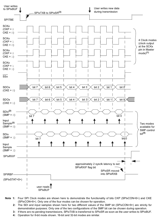
I have this tid bit from a chart in the SPI-specific datasheet:
![]()
It appears to take 1 to 3 SPI bus clock cycles to complete a write to SPIxBUF. Why a range? Well, after 5 SPI clock cycles, the chart shows the user can write new data. If it took only 1 clock to write new contents to the buffer, then the latter 3 bits would be overwritten, no? If I treat this detail as a duty cycle rather than a fixed time constant/delay, then after 10 clock cycles, I can write new data to the buffer in a 16-bit transfer. As the chart is for an 8-bit transaction, I will have to test the accuracy of this theory since I'll be doing 16-bit transactions, the max the SEPS525 display driver will accept in one transaction.
This holds a lot of hope because I have everything *but* the SPI bus running 1:1 with P-Bus which is again, 1:1 with SYSCLK: any cycles the SPI bus isn't occupying the CPU means I have 4x that for calculations, IRQ servicing, ADC sampling, et al. Fingers crossed.
-
Redundancy
05/29/2014 at 16:01 • 0 commentsWhile I wait for parts to arrive tomorrow and take a break form the display board creation which is mechanically more complicated that I anticipated, I have been running the overall design of D-DAQ through my head.
The displays are hooked up via SPI. Normally you need CLK, MOSI, MISO, SS pins for SPI. The SEPS525 requires the MISO pin to stay unconnected when using SPI so I'm using that line for a button's input. I then noted some language in the datasheet about the 2 different SPI modes, normal and framed.
Normal SPI mode will only generate a CLK when the interface is active and need to send data. Framed always generates a CLK and uses the SS pin to send a 1 CLK pulse to indicate a transfer is about to occur. I missed the detail saying that in Normal mode, the SS pin is optional.
I ended up tying all three SS pins to ground as required by the data sheet, and ended up scrounging around the board to find 3 pins for toggling the RS pin on the SEPS525 to differentiate from a command and data. Oops.
The good news is that I have 3 extra pins to play with if the need arises. The bad news is that I'm running unnecessary pins to control functionality. Boards of proto 2 have not been ordered yet so I'll probably fix this in the near future.
-
Prototype 1 Boards
05/28/2014 at 05:55 • 2 commentsIf you saw my bit earlier, you'll know that I received my first set of PCBs today. I setup some time after unwinding from work to grab hi res photos of the boards so it'd be easier to QC areas that I know were very tight on tolerances and could be a problem. Some, like the mDP connectors, are unavailable at this time. Others, I just have to be careful and/or use a lab that has tighter tolerances.
Here are adjusted photos that show the areas I have to examine on each board:
Top side:
![]()
- Traces between C1 and C2 for the 3.3V rail. I copied the basic layout for this SMPS topology from the manufacturer's data sheet as well as I could.
- C3 was a "Ooops, did I really do that?" as it's covered by the inductor. I shouldn't have any issues and fudge the location of both a little.
- MIddle of the board is a via for ground planes.
- Far right are the set of vias that caused me to use the min drill size, 13 mil, to help try and avoid clearance issues. This is for the SRAM chip so it's kinda a show stopper if there is a problem an Xacto knife cannot fix.
- The closest pairs of through hole pads for the mDP connectors are about 2 mil too close. It just dawned on my that I can manually space them further without issue...
Bottom side of the board problem areas:
![]()
- The trace length matching in the upper left have a couple bumps that are very close to their neighbors, but I don't see an issue.
- Vias just to the left are a big concern because I am really tight on space there and used the min drill of 13 instead of the normal 15 for every other small via.
- A particular by pin 1 of the PIC32MX is routed very close to the via and the pin itself buy about 2-3 mils.
- 2 other misc vias
- Diodes are missing polarity silk screens because I put them on top of the traces in the upper right.
- Down and to the left of those, I realized that the accelerometer footprint was well under the tolerances, but they seem to have printed it anyhow. I may or may not add it onto the board on this prototype.
In general, I know that there are no plated slots on the board. They are structurally required for the USB ports and mDP receptacles. At the moment I'm going to live with it and use a dremel to trim the parts a tad.
High res photos of each board, from and back. They are 2000 pixels tall and ~3600-3700 pixels wide. They've been edited for contrast and inspection. If you think you see a problem, feel free to speak up.
Board 1
![]()
![]()
Board 2:
![]()
![]()
Board 3
![]()
![]()
-
Most Parts Ordered, et al.
05/26/2014 at 07:11 • 0 commentsWith the exception of a few outliers, all active components have been ordered. I have enough for 2 main boards, or enough for 1 board and then spares ;), and 3 displays. Since mouser isn't shipping until Tuesday, I'll finish up the passive component wrangling, need to calculate power ratings, and place a separate order tomorrow. Still a hefty chunk of change. I tried splitting up the components amongst 2 or maybe 3 suppliers, but I'd save maybe $10 in this low quantity.
Display boards are not yet complete in schematic capture, let alone board layout, though both have commenced. I'm iffy about the crossover connections on the mDP cables since I'm not sure if the + lane swaps with the + lane or neg lane. I'm assuming the former and have wired accordingly. I can test conductivity with the receptacles when they arrive. The display board design accounts for a breakout board for the mDP so there is a little extra design complexity, though I feel I've sorted it. I'll place this batch of boards through Advance Circuits as there are fewer things to overlook and I need 3x the amount. Time for sleep, then work.
-
LED PWM Frequency, Brightness, & Bit Depth
05/24/2014 at 23:18 • 0 commentsUnless you're new to HaD, you already understand why driving a LED with PWM is really good thing. If you're knew to this kind of thing, it's still relatively simple. It means that you can drive an LED with higher current without burning it out and if you can have a fast enough frequency, you will not see any flicker. However, if you're like me, it's far from this simple ;)
Now I'm designing D-DAQ's displays to accommodate several different types of LEDs. The problem is compounded not because they have different forward voltages, but because they have different steady state and peak/surge/max current limits as well as different pulse widths with those limits. from my minor collection of datasheets, the trend seems to be somewhat linear with a max pulse width of 0.1 ms, 10% DC, 10x steady state current. However, I do have a few outliers that have a max pulse with of 10 us and 6x steady state current. So, for the lowest common denominator and assuming 10% DC since it wasn't stated, it seems that I have to have a PWM frequency of 10 kHz. Thankfully, this is a relatively easy frequency to achieve with a PIC32MX.
There is a little bit of a problem though. As I mentioned in my log from yesterday, my solid state relays have a 10 ms lag before they turn on. I'd rather not go and find another SS relay and add it to Eagle, so using what I have on hand, I open up the datasheet to figure out if there is any way to speed this up. Well, as luck would have it, the 10 ms turn on time is the rated maximum. In the graphs and charts of the CPC1117N, 22 out of 50 units turn on within 0.32 ms and none of the graphs go beyond 0.7 ms for the turn on time for <1 mA drive current. At 10 mA, turn on time is no worse than 0.4 ms.
As for the signal to turn on the SS relay, I've altered my plans and will be using a single p-channel MOSFET on the accent/backlight PWM circuit. From it, I'll be running a 2nd order high pass RC filter in parallel to the accent/backlight LED load so it will always see 14 V, thus not requiring modification when changing the LED load. Now, since this is driving the warning light circuit, I want to ensure that that circuit doesn't come on until I've reached about 10% of the visual brightness of the accent/backlight LEDs. Even though I'm now dealing with a nominal 320 us turn on time, I'm dealing with a max of a 10 us pulse with an off time of 90 us between pulses. Unfortunately this means a simple 5x RC time constant will not suffice. Time to break out the circuit simulators.
I personally like using circuitlab.com. Yes, there is circuits.io surely others out there, but having a browser based simulator, plenty of parts and variants to work from, and a fairly decent UI makes this one my go-to choice. I'm sure it may have it's inaccuracies with the simulation engine, but we'll see how close it is when D-DAQ is constructed and I'm testing everything out.
You noticed how I said visual brightness a second ago instead of DC, right? My background in photography is bit more than a decade and I'm also red-green color deficient. Now, it should be apparent that I'm a detailed oriented person who doesn't mind getting into the technical details, even if I may be wrong. That being said, due to my color vision, I've developed a decent understanding of the human eye's anomalies with light. That being said, I figured it'd be somewhat useful to rung a Google search regarding the LED PWM brightness. Well, as soon as I saw the logistical curve, I knew I had to go a bit deeper into the PWM frequency of choice.
Though the PIC32MX can easily do a 10 kHz PWM signal, there is a relation to the PWM frequency and the Peripheral bus frequency that affects the bit depth at which you can control the DC. Many years ago I used to be active in the ticalc.org community and even with the power of C via TIGCC, the only way to code a fast 3D engine was to use an integer-based trig lookup table. You'd think that 0-255 would be plenty of depth (8-bits in case you missed it) for a curve, but if you're trying to do anything with precision, you'll quickly find that you'll get a heavy amount of aliasing on quick transitions of the curves. Now, looking at the logistical curve of the brightness plot, it's apparent that I'm going to need a fair about of bits.
There is another factor to consider: flicker. At the beginning, I mentioned the frequency to drive the PWM signal at. Now, how do you know if it is too slow? Have you ever been behind a car at night with their brake lights on and you've looked from one side of them to the other so that your persistence of vision allowed you to see the on time and off time of the taillight? Annoying huh? I certainly don't want that to happen with D-DAQ. I give special thanks to a friend of mine who's done some eye tracking stuff back in the day and he quickly confirmed that the human eye can move up to ~900˚/s. The displays I'm making will have an average distance from the users face of about 2 ft, give or take. My personal limit to having flicker noticed at this distance is something I'd set to about 1-2 mm. Recall that the minimum off time of the LEDs at 10 kHz @ 10% DC is 90 us? This works out to 0.86 mm when you run the trig. Going to 1% DC, that gets up to ~0.95 mm. If I doubled that distance, we'd be talking about 5 KHz, which has the possibility of being too slow. Lucked out there, eh?
Well, this next pondering is what brought me into this whole post. A max DC of 10% which means 10% of the available bit-depth, couple with the appropriate transfer function recalling those bits to fit the logistical LED PWM brightness curve. I had to pull up the datasheet for calculating the available bit depth of a given PWM frequency. Turns out it's tied to the peripheral bus speed. After running the numbers, I get about 12.67 bits or a highest value of 6547 and 10% of that is 654, or ~9.4 bits. If I were at 5 kHz, I'd have a max of 1309. As we're dealing with logarithms (human vision) the logarithmic median between those two is ~926 which gives me a wonderfully oddball frequency of 7.07 kHz. I know my 14 V rail isn't strong enough to drive everything at full power so derating LED currents is okay with me. Oh, and dumb luck that it's a reminder of sqrt(2)/2, used for RMS calculations ;)
Anyhow, back to the original problem of an RC circuit turning off at of at a visual brightness of 10%. A common formula that has been derived for this calculation is listed here. After some trial and error I found 3 flaws that were easily fixed. First off the divisor, 21 in the example, is actually the rounded half of the max value, 255, divided by the offset value 6. Second, you'll never hit the max value due to the nature of a logistic function so you need to use the number of points you're plotting, i.e. 8-bit = 256. So, using the range 0-925, the max value 926, I solved for the divisor that would get me to 925 without having to round up, thus giving me the maximum dynamic range of the function, which turned out to be ~6.8446. I plugged 0 back in with the divisor at got ~0.9853. I subtracted half of this value to remove the offset and got my tabulated results.
Last note, if you wish to just run an 8-bit table, the divisor with the maximum dynamic range is ~5.5849 and subtract 0.4787 from the result to remove the offset.
Edit: If you choose a divisor greater than what I've stated the curve will become more dramatic and steeper. If you choose a values smaller, then it'll be more linear. Keep in mind though, that it is not possible to create a "linear" "curve" from this type of function. If you wish to use this function to play with or compute your own tables other bit depths:
=ROUND(($A$2)/(1+EXP(-(A4/($A$2/(2*$B$2))-$B$2)))-offset,0)
Where A2=points (which is 2^(bit depth) in case that isn't intuitive) and B2=divisor
To compute the divisor with the greatest dynamic range use:
divisor = -points * ln( 1 / ( points - 1 ) ) / ( points - 2 )
Edit 2: I was a bit mentally exhausted and distracted from the primary goal after running that math so I missed following through to the final conclusion: I need enough bits to scale the PWM DC smoothly enough to have visual brightness vary smoothly. 926 levels are nice, but I'm running at 10% DC, thus I'd only have 92.6 levels. In order to expand that to 100 levels, PWM frequency would be limited to ~6.547 kHz. I wish I could make the CPU faster, but at this time, the clock dividers and SPI frequency limits make that a non-option.
To limit a PWM pulse to 10 us, I can only go up to 66 of the 100. I'm still under my 2mm upper limit for distance traversed upon rapid eye movement, ~1.46 mm, so I hope flicker won't be an issue. At the same time I'll be happy to test to see if the LEDs will survive at a 15.3 us pulse at 10% DC though.
-
Display Brightness Control
05/24/2014 at 18:26 • 0 commentsWhether I use an SEPS525-based display or a SSD1353-based display, there is a pin on both controllers called I-ref. This is an internal current reference for brightness control. Its nice that the SSD1353 data sheet gives a transfer function for how to use this resistor, larger values decreases brightness, but the SEPS525's sheet, albeit from the controller datasheet of a display model datasheet, has no reference of it's own.
That being said, I have long since planned using this pin to control display brightness. I knew I wouldn't have a control line from the mainboard to each display that I could use to flip a switch and dim the display. Also, that kind of digital interface usually has by nature or is created with a delay in response time of several seconds, which is something I personally despise. I could also go with running a trigger wire from headlight activation for dimming the displays, but it's so much less elegant and "dumb" in comparison. Anyone who'd driven knows that light doesn't hit the interior of a car in a uniform fashion and that is why individual, fast response of the display brightness matters to the design.
In conjunction with not knowing if the resistance is proportional, inversely proportional, logarithmic, or exponentially related to display brightness, I cannot predict when and by how much the display will dim or brighten. So, upon realizing this nearly a year ago, I knew I had to find a way to create an analog roll-off of the brightness with a simple circuit. After a few days of research, I settled on the APDS-9007.
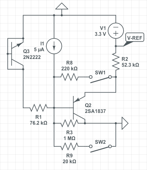
This little guy has a current output from 5 uA to ~46 uA and by nature of the load resistor, turns that into a voltage for an ADC. Dedicating 3 ADCs is overly complicated so as I'm working on the display boards, a discrete solution needed to be found. After a little bit of research, I learned that BJTs don't mind such low current drives to their bases so all I had to do was figure out a good way to bias it properly. Oh, and since I don't know if an increase or a decrease in I-ref will dim the display, I need the circuit to do both.
Well, I decided it would be overly complicated to have both an NPN and PNP resistor on the PCB along with 2 jumpers and 2 possibly used or unused resistors, so I setup the circuit to just include or exclude the biasing resistors for one transistor. This is equivalent to removing or including 2 parallel resistors on board so it takes up the space of only 2 extra resistors. Here is the circuit:
![]()
You can ignore the defunct BJT in the upper left. It's there so I do not have to delete and add the transistors over and over for simulation testing. The constant current source, I1, is simulated with the weep or 5 uA to 45 uA and the switched behave as 'jumpers' to where I can simply remove them in real life as I mentioned above. R1 is the load resistor on the light sensor. I'm also making a huge assumption about the reference voltage being 3.3 V inside the SEPS525. It could be 14 V or it can be a self-generated reference voltage. Either way, this circuit should give me an idea of the response range and type, linear or logarithmic or exponential, so I can add it into the final design.
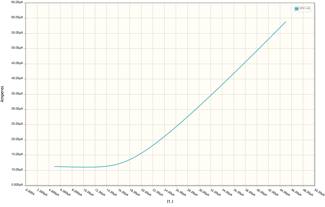
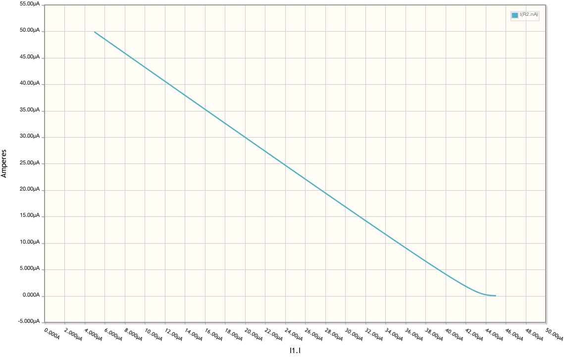
The responses are as follows. I wish I could have made the ramp up more linear, but it'll suffice. I'm also making an assumption on the SEPS525 based on the SSD1353: There is a limit to the maximum current that I-ref should be. I can overshoot that max a little, but since the initial testing will be indoors, so it's easy to control the lighting and figure out some semblance of a response curve.
Ramp Down response:
![]() Ramp Up response:
Ramp Up response:![]()
-
Display Lighting - Working with Limitations
05/24/2014 at 01:47 • 0 commentsEach display will be accompanied with 2 sets of LEDs: one for accent/backlighting, and the other for warning if a parameter gets [too] close or surpasses a use defined level. The catch with this was that I don't have various "control" lines to run over to each back of LEDs to turn one set on and another off and I'm using 3 colors on 2 PWM lines. Things became a bit tricky.
MOSFETs. And here I thought op amps were a pain... I quickly came to realize that I needed both an n-channel and a p-channel MOSFETs to act as normally open and normally closed switches. I could use the solid state relays I've come across, but those are $1-$1.50 a piece and 2 MOSFETs in 1 package of equivalent rating are less than 1/3rd to 1/2 the cost and have better thermals. Plus the SS relays have an switching times of about 10 ms where as the FETs are a few orders of magnitude faster.
The delay in creating the display boards is this circuit, though I've not explained what it does. My warning LED is a dual color, yellow and red, LED with a forward voltage of 1.95 and 2 v with a driving current of 20 mA. I don't need both on at the same time, but I only have 4 PWM lines. I've divvied them up to 1 line per display for the warning LEDs and the 4th line as general accent/backlight control. I ran across a problem in my theory of driving that dual-color LED: I could never have both turned off at the same time. This is even if I dial up the frequency and let the input/output capacitance of the FETs limit the on-off time as when that happens, the average voltage just climbs.
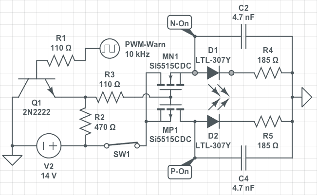
Well, I was ignoring one fact: I have the accent/backlight PWM line I can use. To minimize visual clutter, I'm in favor of turning off this light when a warning light comes on. Since those accent lights would be driven only part time, I would just need to use the on/off duty cycle to trigger to solid state relay. I was hoping to avoid using any of the SS relays, but hey, they are functional and a 10 ms delay before tuning one on isn't that big of a deal when I'm not rapidly changing its state. With that being said, I just needed to figure out some control circuits for driving the LEDs and below is what I came up with:
![]()
It's relatively simple circuit, modeled after the high-side load switch topology. The PWM signal rapidly turns Q1 on and off pulling the gates of the FETs to ground. R1 and R3 are current limiting. R2 is a pull down for the source of the N-channel FET so it can turn off, else it'd float on. If the value of R2 is increased above ~470 ohms, the capacitance of the FETs interfere with each other and alter duty cycle and on/off time of each other with a preference of keeping the p-channel FET on longer. I'd prefer a larger value, but I already have a limited 5-90% duty cycle due to roll off. R2 will have to be at least a 1W resistor. I updated the models with the info for the Si5515CDC dual FET from Vishay (pdf link). The caps, C2 and C4 are bypass caps to reduce the voltage spikes when the switch is open and the PWM signal is still active which is caused by overlap of the p-channel FET's slow turn off overlapping with the turn of the the n-channel FET. As they affect on-off time as well, I increased them to where their effect was minimal, but limited the transient spikes to about ~1.3V and ~-1.5V. SW1 will be replaced with the SS relay controlled via the accent/backlight off-time duty cycle, basically making it a low side switch so I don't have to worry about heat dissipation. The LED and current limiting resistor pairs are placeholder for the series/parallel/mixed LED arrays for the displays.
The highest draw LEDs that would be powered have a forward voltage of 4.9V, and a drive current of 20 mA. I'd need to drive 4 of them requiring 9.8V and 40 mA. I'll be using my 14V rail for juice and the Si5515CDC can give me at least ~55 mA @ 14V continuous at 50˚C, which is my internal maximum temperature threshold.
If my nomenclature is incorrect a couple paragraphs above, I blame it on not fully understanding the voltage relations of the source, drain, and gate on the FETs ;)


 Ramp Up response: