This Micropython class handles a single button and provides two possible events: Pulse and Long press. It also provides debouncing.
The .event( ) method shall be called at every execution cycle. The constants for debouncing and Long Press thresholds must be proportional to the timing desired. In the example the function is called every 5 ms. Any pulse that lasts less than 50ms is considered as a bounce and hence discarded. If the button is held for more than 500ms the function returns a single LONG press event.
Finally, if the button is pulsed within a time 50ms< t < 100ms the function returns a PULSE
from machine import Pin,
import time
print("Button Handler Class")
classbuttonHandler:def__init__(self,pin):
self.pin = Pin (pin, Pin.IN, Pin.PULL_UP)
self.tOn = 0self.tmp = 0self.evnt = None
defevent(self):
ifself.pin():
if (self.tOn <10): # does the key get pressed for at least 10 scans ?self.tOn=0# no, it was just a bounce, ignorereturn None
else:self.tmp=self.tOn # yes, save amount of scans self.tOn = 0# and reset counter if (self.tmp < 100): # does the key get pressed for less than 100 scans ?return1# yes, it was a pulseelse:if (self.tOn < 500):
self.tOn = self.tOn + 1# restrict max value, just in caseifself.tOn == 100:
return2# return long only oncereturn None
b = buttonHandler (12) # instantiate and init pinwhile1:
bte = b.event()
if (bte):
if (bte==1):
print ("short")
elif (bte==2):
print ("long")
time.sleep_ms(5)
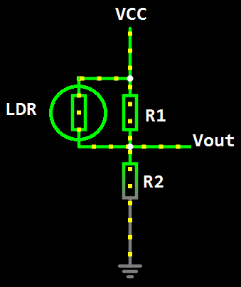
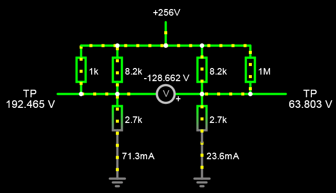
An LDR's resistance, RLDR can vary from about 100Ω in the sun light, to over 10MΩ in absolute darkness (source).
For practical uses we can consider one order of magnitude above and below the extremes, which in numbers means a resistance variation range from 1KΩ to 1MΩ.
With that in mind it is possible to use the LDR along a voltage divider circuit and calculate the values of the resistors so the output voltage will match a desired range as long as such range is reasonably within the voltage rails, for instance, In a recent project I needed to use the LDR reading from an 8 bit ADC to drive a 5 bit soft PWM, then a range of 128 counts could be easily shifted right to get me the values from 0 to 31 (and avoid a floating point division math).
We have then 2 unknown variables, R1 and R2 and two known resistance values and their expected output:
LDR in dark, R = 1MΩ, Vout = Vdark
LDR in brightness, R = 1kΩ, Vout = Vbright
It is reasonable to consider that Vdark and Vbright will be symmetrical around Vcc/2, and to perform the calculation of the resistors we can normalize the voltage value to the resolution of the ADC (e.g. use a value of 256 in the math instead of 5V).
Rewriting the terms, considering the half of the ADC scale is 128 and half of the desired range is 64:
LDR in dark, R = 1MΩ, ADCount = 128 + 64 = 192
LDR in brightness, R = 1kΩ, ADCount = 128 -64 = 64
That can be solved using the voltage divider equation:
There are several ways to perform the math, including Wolfram Alpha, and the equation to find the resistances can be calculated using the following string
The calculated values will hardly be an exact value, but the E24 series can provide values close enough to get the desired counts from the ADC
Resistor
Calculated Value
Closest E24 Value
R1
~8072Ω
8K2 Ω
R2
~2669Ω
2K7 Ω
It is possible to use the Falstad online simulator to check how good the picked values are, and of course to fiddle with the values. To save time it is possible to use the link below the access the simulation.
INotice that the Vcc voltage was set to 256 to make it easy to check the ADC count values from the LDR in brightness (left) and in darkness (right). The difference between readings is shown in the middle. Also notice the E24 series values provided good results (no need to use precision resistors)
Epilogue:
if the LDR is exposed under extreme conditions the resistance values canreach the maximum values and the voltage range will differ from the calculated, therefore it is necessary to limit the range in software. It will also be necessary to subtract the value from the minimum expected value to have a light reading value starting from 0 (zero).
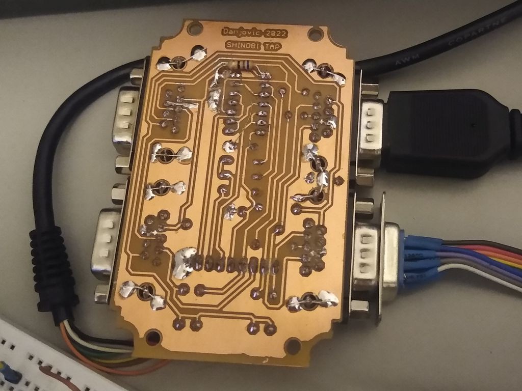
After a suggestion from [gdx] from MRC I took a look at the Rock'N'Roller (MSX1) and started to work on a patch for Ninja/Shinobi Tap multi controller adapter.
First step was to disassemble the game and figure out how the game deals with the controls. There are several calls to 3 of the BIOS routines that read the keyboard, the joysticks and the trigger buttons (from the joysticks) and decided that the best strategy was to emulate such BIOS routines and return correspondent values based on the buttons pressed on the controllers plugged in the multitap adapter.
Next step was to figure out a position in RAM out of the game execution to place the patch code -> address 0xdf00 to 0xe300 seemed nice
Following I have created the alternate routines:
ALT_SNSMAT
ALT_GTSTCK
ALT_GTTRIG
The alternate routines fall back to the original BIOS call when the Ninja/Shinobi tap is not detected (a flag is reset) . for instance...
ALT_GTSTCK:
    ld b,a                  ; save row number
    ld a,(ninjaDetectFlag)  ; test for ninja presence
    and a                   ;
    ld a,b                  ; restore row number
    jp z,0d5h ; (GTSTCK)    ; if not present continue with BIOS routine
    ;
    ; read and return STICK value
...
Next step was to generate a list of addresses where the BIOS calls are called and write a quick and dirt and code to replace such calls with the alternate routines created. The +1 is the offset for the instruction code CD (call) at the addresses that call the bios routines.
; Patch Original game code
    ld hl, ALT_SNSMAT  ; patch calls to 0141h (SNSMAT)
    ld (09648h+1),hl
    ld (0966bh+1),hl
    ld (09676h+1),hl
    ld (09685h+1),hl
    ld (09b7ch+1),hl
...
Then I have created a function that will be called in the game main loop to scan the joystick ports and detect the presence of a multitap adapter om port A. If an adapter is detected, a flag is marked and the four taps are read and converted as a mirror of a keyboard matrix and joystick directionals and triggers.
NINJAPATCH:
	; check for presence of Tap
	call CHECKTAPS ; c = 0  0  0  0  a1 a0 b1 b0
	cpl            ;  c = 1  1  1  1 /a1 /a0 /b1 /b0
	and 08h        ; isolate bit a1 ->  a = 0 0 0 0 /a1 0 0 0
	ld (ninjaDetectFlag),a  ; /a1 should be 1 if a ninja or shinobi is detected
	ret z

; scan taps
;   ld de,0fa7ah  ;  Tap connected to joy port 2
   ld de,0ba3ah  ;   Tap connected to joy port 1
   ld hl,ntapData
   call GETNIN ; read TAPS on port 1

; process taps *************************************
...
Button Mapping
Tap 1 is mapped as :
Up, Down, Left, Right -> Ditto
Trigger A - Z
Trigger B - X
Select - SEL
Start - Escape
That was done to allow full access and control of Options menu from the game, but it is still possible to access and control the Optiosn menu using the MSX keyboard.
Tap 2 is mapped as the QSCS (Q, S, Control, Shift) controls
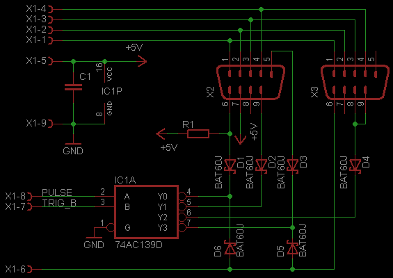
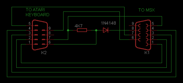
I have built the Atari 2600 controller keyboard DIY to develop an adapter and write a driver for MSX. The adapter aimed for simplicity but it does not provide any detection feature, requiring the user to without an action, either pressing a key or move the joystick to any direction, depending upon the peripheral connected on the joystick port.
If I give up the simplicity and add an Integrated Circuit and a bunch of diodes it is possible, though, to build an adapter that can support both the keyboard controller and a single button joystick, connected at the same time, using basically the same driver. And there's more: the joystick can still be read by Basic.
here's the circuit:
The rows of the keyboard connected at X2 are selected by the pins PULSE (8) and TRIGGER_B(7) (which is bidirectional). The default state of these pins are PULSE->0 and TRIGGER_B->1 which selects the common line of the joystick, thus allowing the single button joystick connected to X3 to be read using BASIC.
Detection is possible by Selecting the third keyboard ROW, then diode D5 will bring down the level on the TRIGGER_A line. The other keyboard rows will keep this line high.
I have created a ROM version of Muhonmourn3. It was necessary to move the game to RAM because the game uses contiguous areas to store data (and some areas beyond 0xd400 too).
Additionally, it was required another routine to switch back page 1 from the Game ROM slot to the same slot of the BIOS, otherwise the game ran erratically (slowed down and missing time counter and player counters).
The ROM -> RAM loader is very primitive but it seems to be working fine in many emulated machines.
The loader executes the following steps:
Check if the computer has enough RAM to load the game
Load a Splash Screen (or a NO RAM screen advice)
Copy patch code (from page 1) to RAM segment E000-E1F0
Copy game code (from page 1) to RAM segment c000-d400
Copy game code (from page 2) to RAM segment 8000-bfff using RDSLT
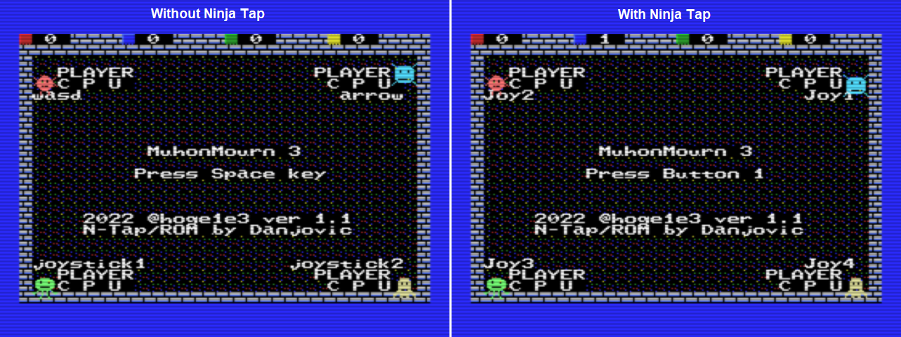
The patch was modified to change the text on the screen accordingly with the Ninja Tap presence:
The whole repository can be found at my github page, and here's the link for downloading the ROM image.
Splash Screen
The ROM loader adds about 2 seconds to the startup of the machine running the game, then a Splash screen was added to divert the attention and reduce the perception of the loading time.
The Splash screen uses Screen 3 multi-color mode, with a resolution of 64 x 48 pixels. The image was edited using mspaint and the space color was reduced to 16 colors indexed mode (bitmap) using irfanview, then a python script to convert the pixel information into data to be included on the loader code.
The screen 3 mode uses 1 byte to represent the color of two pixels (each nibble is a pixel color). The whole screen takes 1536 bytes which is the half of 64 x 48 -> 3072 pixels available.
The pixel addressing is not linear but with a bit of observation it is possible to assign the values of the coordinates X and Y to certain bits on a linear addressing word:
The color translation was done kinda manually, assigning the the indexes informed by clicking on the image opened on Irfanview to the desired MSX color.
The main function iterates over all 3072 pixels, combining every 2 of them and generating the contents for a include file, skipping a line every 32 pixels (16 bytes).
for i inrange (0,1536*2,2):
x,y = getCoords (i)
pp = translateColor ( pixels [x,y] ) # get MSB color
x,y = getCoords (i+1)
ss = translateColor ( pixels [x,y] ) # get LSB color
bb = (pp<<4 | ss ) & 0xffif (i % 32 == 0 ):
outputBuffer = outputBuffer + "\n db "else:
outputBuffer = outputBuffer + ', '
outputBuffer = outputBuffer + intToHexValue2digits (bb, '$')
print (outputBuffer)
At the end the result is printed on the terminal and can be copied and pasted on a text editor.
It is a very crude script but it was enough for me. It is impressive what we can do with 40 lines of python ( nevermind the blank lines and comments)
Screenshots
The splash screen depends upon the slot where the ROM is inserted is even or odd. Both were inspired in Rock Bands.
Even Slots: QueenOdd Slots: Information Society
As it was mentioned before, the game needs at least 32K of RAM to be copied to memory. On some machines without RAM expansion the No RAM splash screen is shown
Advert for machines with less than 32K of RAM
Worth to mention that after the splash screen was added it was necessary to add 3 more seconds of delay...
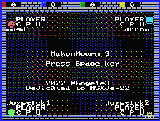
The game Muhonmourn 3 is a multiplayer game developed developed by [hoge1e3] as an entry to MSXDev22 contest. The game allows up to 4 players, being two on keyboard (using arrow keys and WASD) and two on the joystick ports.
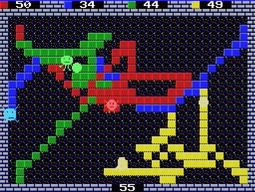
The game dynamics is simple but very addictive. On every match you have 60 seconds to control your player to cover as many ground as you can during 60 seconds.
I wish this kind of game existed when I was young, on the occasion when we, our brothers and friends get together to play video-games.
Today this is a game that is perfect for retro meetings and that was my motivation to research about the obscure peripheral named Ninja Tap that allows to use up to 4 joysticks by port, in other words a multi-tap adapter.
At the beginning there was no much information about this peripheral, and I have started to look for information on how to reproduce such peripheral and find out how it works and how to write software for it. The whole story is on a series of pages here in hackaday.io (btw, thanks [Jipe] and [aoineko] )
Some games may also read the controllers directly using the Z80 instructions IN and OUT (that was not the case).
It was found a function starting at 0x865c that reads the eleven rows of the keyboard matrix using SNSMAT routine. The readings are inverted so a pressed key is represented by a "1".
Then the game reads both both joystick ports using GTSTCK and GTTRIG. The directionals are used on a table entry to convert the value read from bios in the range 0..8 to the four upper bits representing each directional with active level in "1". Then the triggers A and B are added to the bits 0 and 1 respectively. The position of these bits corresponds to the row Y8 of the keyboard matrix.
The scan is stored into 13 consecutive bytes starting at 0x86b9
The Patch
The patch code consists of a jump to a function placed after the main game code that perform the following steps
Check the presence of a Ninja/Shinobi Tap on joystick port 1 ( only port 1 to simplify the code)
Return to execute original code if a tap is not detected, otherwise..
Read the Taps
Convert Tap 1 data to "RG DW UP LF 0 0 TB TA" and store at 0x86c1 (row 8)
Convert Tap 3 data to "RG DW UP LF 0 0 TB TA" and store at 0x86c4 (Joystick 1)
Convert Tap 4 data to "RG DW UP LF 0 0 TB TA" and store at 0x86c5 (Joystick 2)steps 4,5,6 conversions are performed by a lookup table that uses the 4 least significant bits as the entry, followed by the bit test of the trigger buttons
Get Tap 2 data an fulfill WASD positions at keyboard rows rows 2, 3 and 5
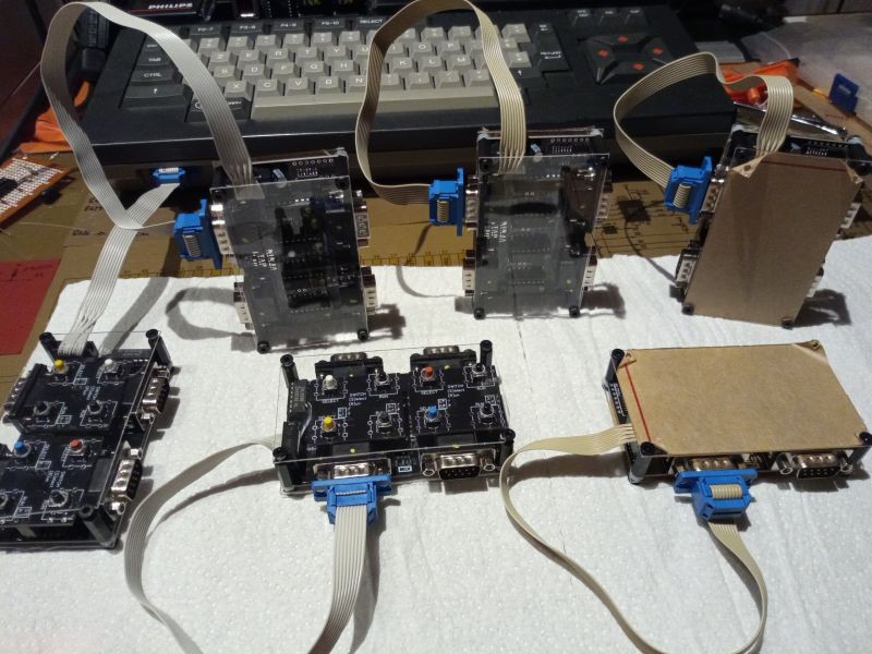
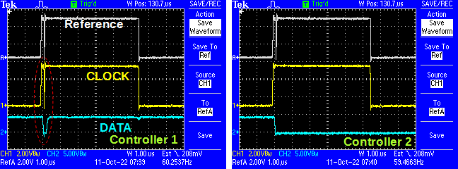
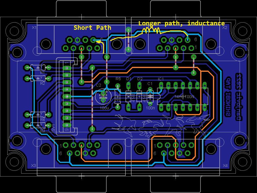
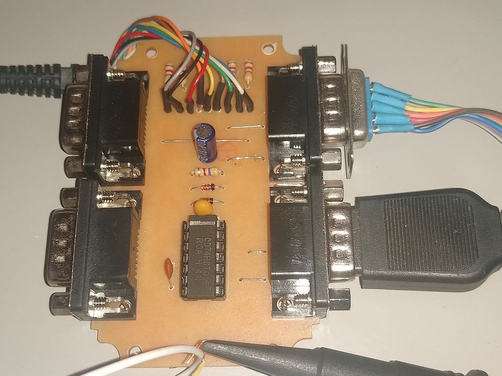
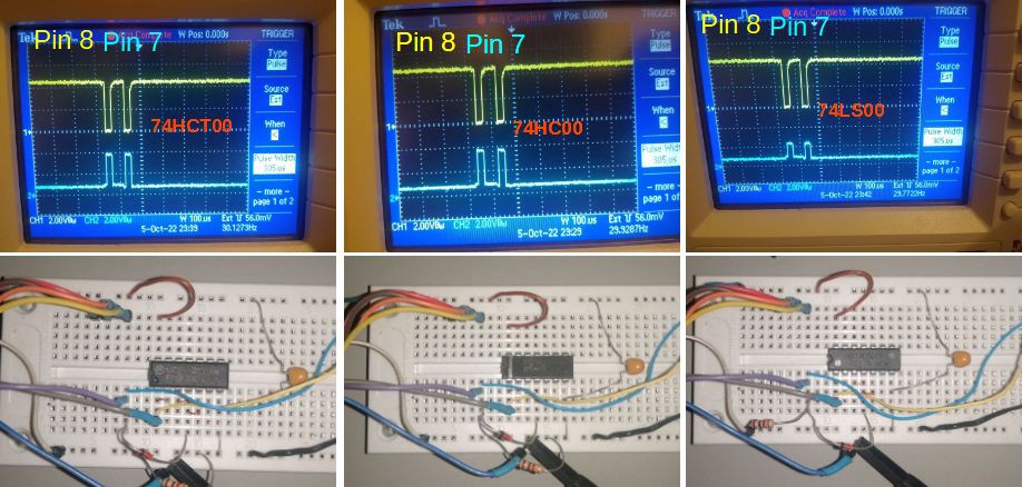
I have assembled a prototype for the shinobi tap and during the tests I came across a tricky problem: One of the famiclone controllers worked erratically when connected on position 1. All wiring was checked twice and it was OK.
Exchanged the port where the interface was connected and same results. Exchanged data wires from controllers 1 and 2 and same results.
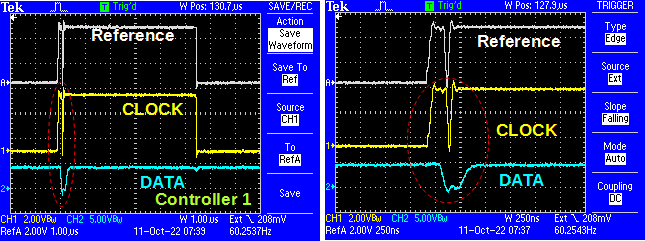
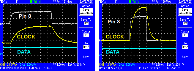
Observing the waveform on a scope it was noticed that the voltage briefly dropped when a button was pressed, instead of keeping low until the next clock pulse.
A closer observation on the waveform at the moment of a button press revealed the culprit: A short surge that happens when the voltage drops at the output and makes the clock ring. The same effect occurs with both controllers but only one of interpreted this as an extra clock.
On the other ports the ringing is barely noticed.
I was suspecting that the ringing was happening only on port 1 because of the proximity with a low impedance source (the electrolytic capacitor at the input). but some tests I have done later proved I was wrong.
I have tried without success:
Added some capacitance to the Vcc line.
Replace the VCC jumper wire with an inductor
Added a 100 Ohms termination resistor on the pin 4 of the Port 1 (CLOCK)
Add some resistance in series with the CLOCK out pin (3) of the HCT00
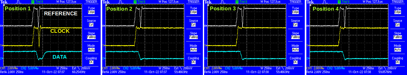
Later I noticed the the other controller (that works despite the ringing) produces the ringing when connected to ports 1 and 2 but not when connected to 3 and 4.
Another thing I have noticed is that when more than one controller had the same button pressed, the ringing was deeper and last a little longer.
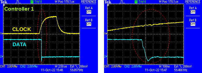
Added a 100nf capacitor (value picked at random ) between CLOCK and the ground. This time the ringing disappear and the circuit worked despite the clock signals turned into triangles.
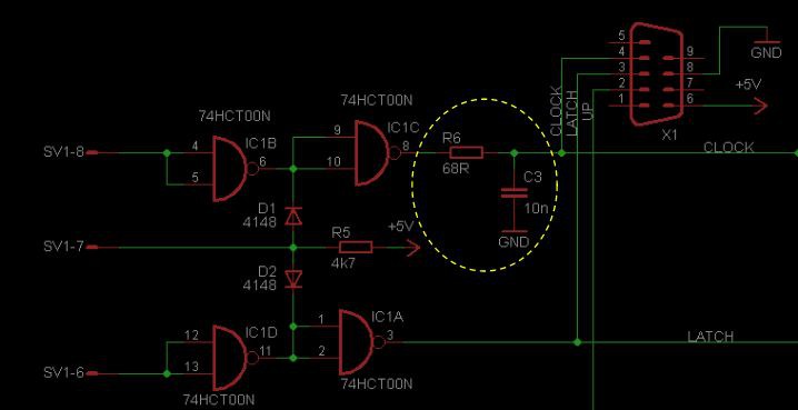
Then I have analyzed again the width of the clock pulse and the duration of the ringing to determine an RC constant to be added between the HC00 and the CLOCK line. The Clock signal takes 6us and the surge around 250ns.
Then I pick a 68 Ohm resistor and a 10nf capacitor to have a time constant of around 680us and added to the circuit, and now the ringing completely disappeared.
Wafeform of the ringing free clock signal
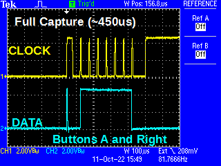
Picture of a full capture
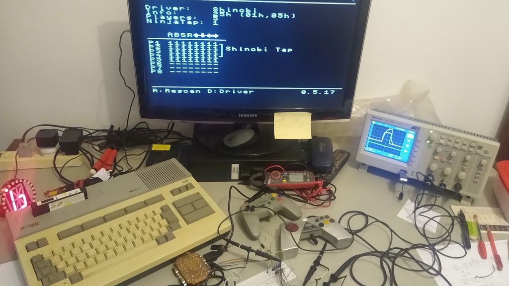
Pictures of the setup
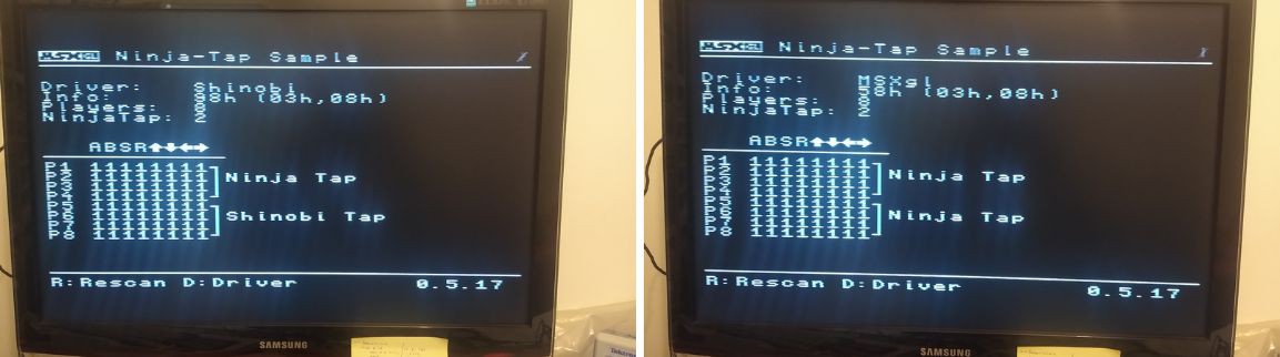
Some screens during test
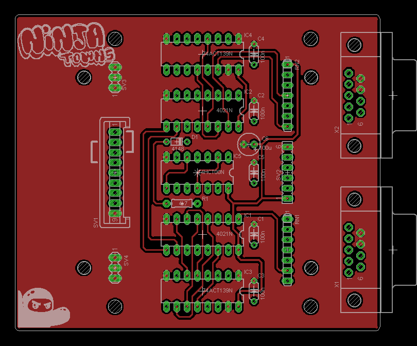
And a closer picture of the prototype. Notice the 10nf ceramic capacitor at the left of the HCT00.
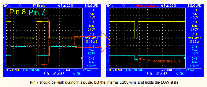
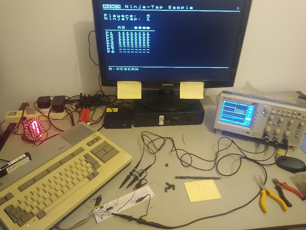
Got some time today to investigate the behavior of the original circuit, as well as the fix I have proposed.
I don't have one ACT chip, unfortunately, only got my hands on a 74'00 from HC, HCT and LS families.
Used the s_ntap program by Guillaume 'Aoineko' from MRC.
As predicted neither one of the three chips is beefy enough to win the fight against the open collector gate inside the MSX, and because of that the software can not "see" on pin 7 the inverted output from the signal on pin 8.
Then I patched the software to keep pin 7 high during the detection routine.
It takes two bytes on CKNTAP function and one byte at CHECK function.
CKNTAP:
 di
 ld  b, #0 ; b=Max Player
 ld  de, #0xBF0A   ;#0xBF00  <-Here
 call CHECK ; Port1 Check
 ld  c, a
 ld  e, #0x4A ; #0x40 <-Here
 call CHECK ; Port2 Check
 rlca
 or  c
 ....
 ....
CHECK:
 call PORSEL
 inc  b
 and  #0xCA ; #0xC0 <-Here
 out  (0xA1), a ; 6,8=L 7=H
 ex  af, af'  ;'
 ld  a, #14
 out  (0xA0), a
 in  a, (0xA2)
 and  #0x20  ; 7=H ?
 ret  z
 ....
 ....
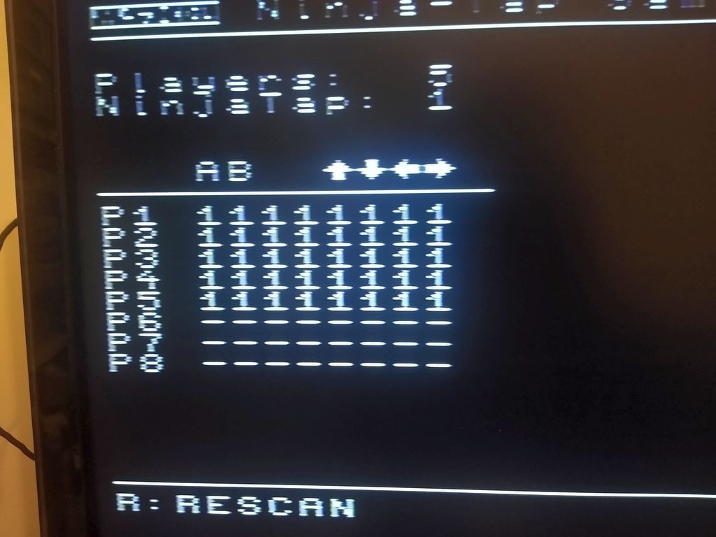
After that, success..
The program can identify a Ninja-Tap connected with either logic family tested.
And it works with either Ninja Tap or Shinobi Tap feedback loop
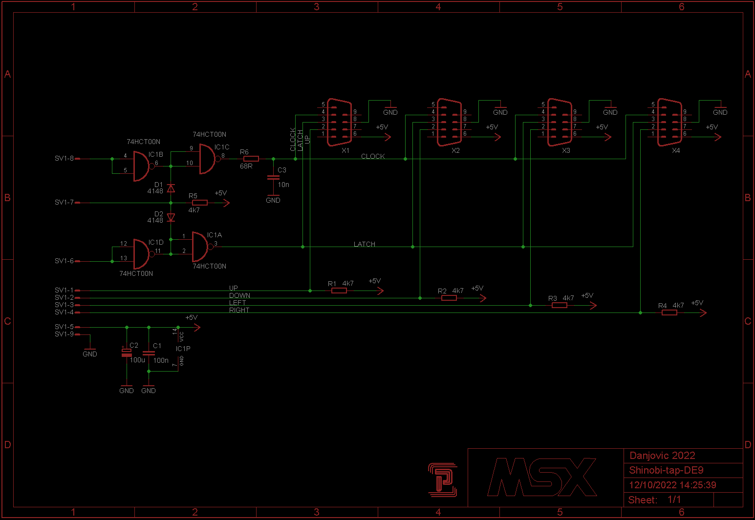
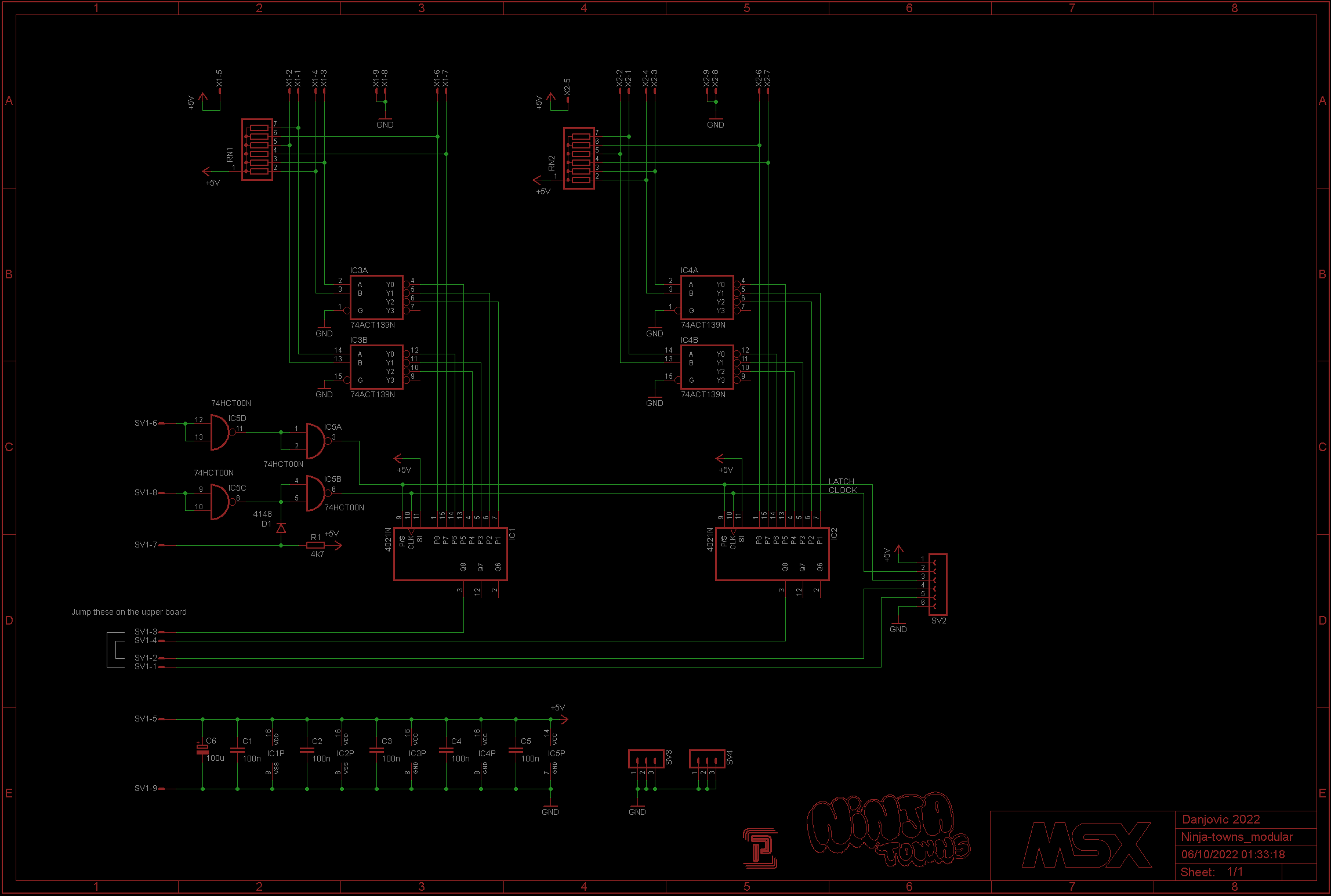
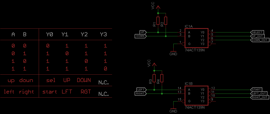
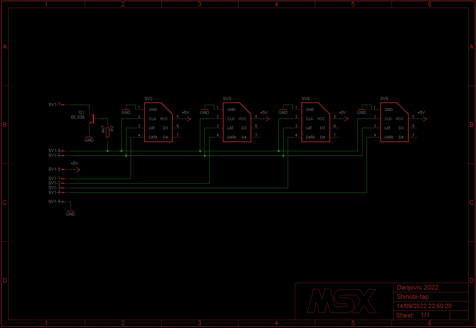
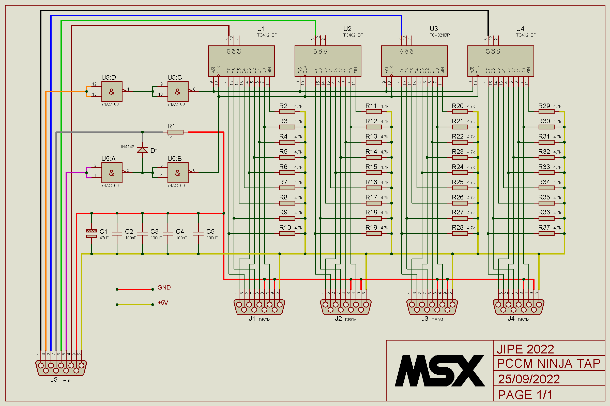
Luckly I was on the right track, being the most relevant difference the SI inputs of the 4021 being pulled up instead of down.
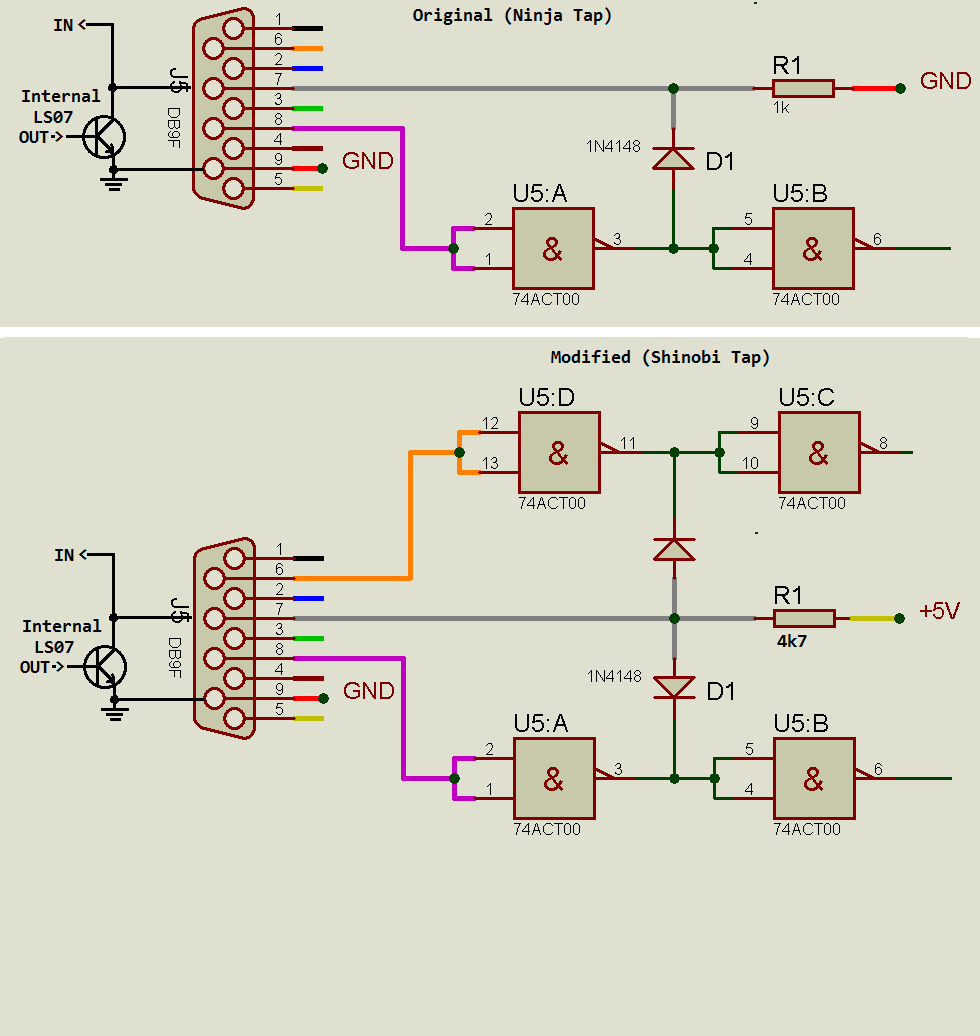
The original circuit uses a 74ACT00 chip not only to feedback the inverted state of signal of pin 8 (pulse) but also to drive the 4021 CLK and LATCH signals (maybe this was the main purpose of the '00 chip).
I have found another error on my circuit. but it was due to lack of attention. Pins 6 and 7 on the input ports were inverted, as D7 on the 4021s shall read the signal of Trigger A and D6 should read Trigger B, not the opposite.
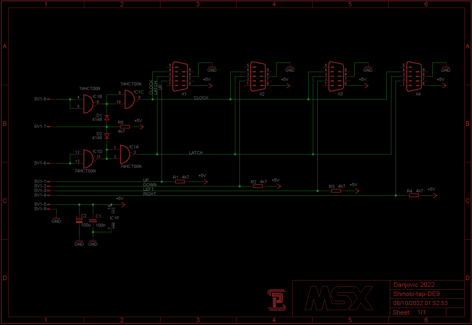
The redrawn schematics is show below:
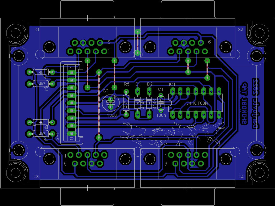
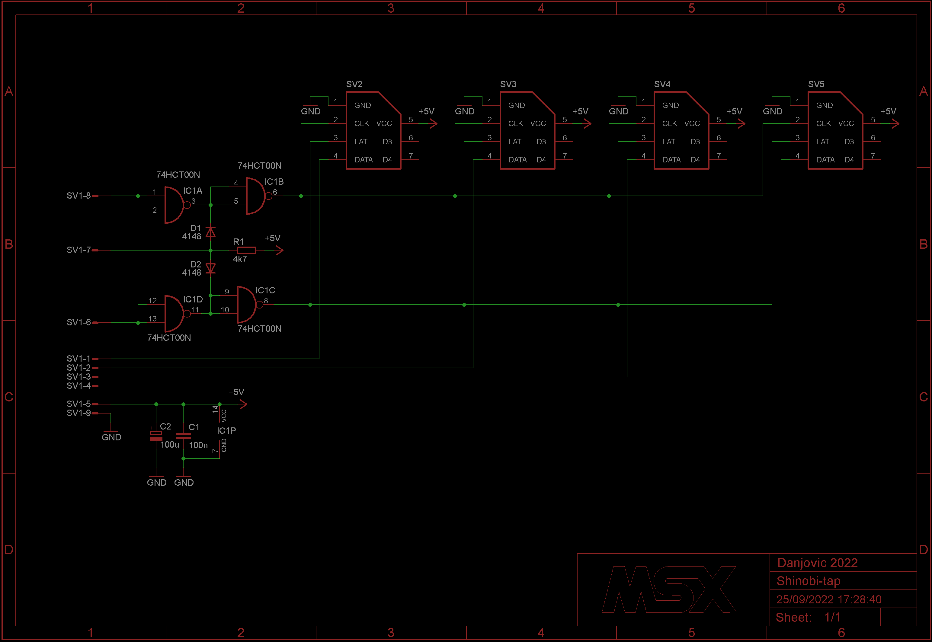
I have also updated the schematics for the Shinobi Tap, but changed the design of the feedback circuitry to avoid contention, and added a second feedback to allow differentiation between Ninja Tap and Shinobi Tap.
Detection can be performed using the expected states. First set pin 7 to High to release the open collector output at this pin.
Sketch for the schematics of a driving controller compatible with Atari 2600 and MSX at the same time.
The circuit uses a rotary switch with integrated push button, and one extra button.
The integrated switch for the rotary encoder connects pin 9 (GROUND on MSX) to pin 7 (Trigger B on MSX). The common return for the extra push button and for the rotary switch is on pin 8 (PULSE) that is driven low by BIOS by default.
When used on Atari 2600 the integrated button works as a positive drive the right paddle input, pretty much like the thumb button on the omega race booster grip (or the LEFT button of a 7800 controller).
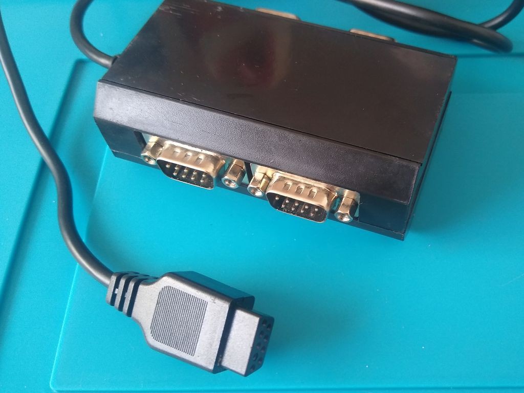
The Ninja Tap is an adapter that allows to use up to 4 joysticks per MSX port (MSX Wiki). There is not much information available on such adapter, let alone the schematics. I wanted to build a clone of such adapter then I have started to disassemble a driver code and translations of japanese documentation available to figure out the connections.
Pin MSX Joystick
Function
6
goes to PARALLEL/!SERIAL of all 4021s
8
goes to CLOCK of all 4021s
7
receives the inverted level of signal from pin 8 (see oddity below)
1
receive the data out from the first tap port
2
receive the data out from the second tap port
3
receive the data out from the third tap port
4
receive the data out from the fourth tap port
5
is the VCC (5 Volts)
9
GND
Protocol
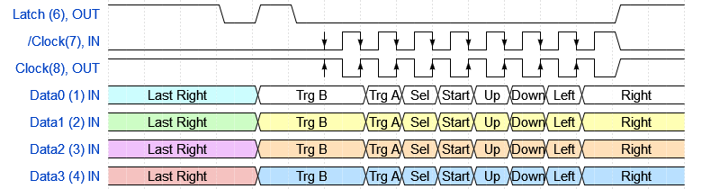
The adapter uses four CD4021s to shift in the controller data from the four controllers:
disassembling the GETNIN function : The sequence for reading the 4021s is the following 0) the sampling start with pin 8 (CLOCK = HIGH) and pin 6 (PARALLEL/!SERIAL = LOW)
pulse (go high, then low) the PARALLEL/!SERIAL line (pin 6). That will latch the input of the keys to the 4021 internal flip flops. Notice that the CD4021 output is already loaded at the Q8 output.
Pulse (go high, then go low) the CLOCK line (pin 8). (note: If this pin weren't initialized high, the first bit would be missed)
shift in one data bit from TAP 1 at the UP line (pin1) into register H
shift in one data bit from TAP 2 at the DOWN line (pin2) into register E
shift in one data bit from TAP 3 at the LEFT line (pin3) into register D
shift in one data bit from TAP 4 at the RIGHT line (pin4) into register C
Repeat steps 2 through 6 for until all 8 bits are read
Process the data.
The sequence of bits is the same used by NES controllers, being possible to make an adapter that uses 4 NES controllers with only one inverter (which makes me wonder to reuse a JoyMega adapter to create a Ninja Mega Adapter)
Oddity
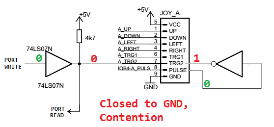
The adapter was designed to be detectable by the driver, and uses the inverted state of signal at pin 8 which is applied to pin 7. The driver flips the state of pin 8 and check if inversion occurs on pin 8.
The problem is that pin 7 is an open collector and the detection routine pulls this pin down (instead of let it float ) during the detection, which means that the external inverter will have to fight (and win) against the internal 7407 open collector gate, otherwise the detection will fail.
Here's the code
;======================================
; Connection Check Sub.
; return with B=B+1 if no hardware detected
; otherwise return with B=B+4 if hardwar detected
CHECK:    CALL    PORSEL   ;
    INC    B          ; B = Max player number + 1
    AND    0C0H       ; A is state of port 15.
    OUT    (0A1H),A    ; 678=L  for both joystick ports (!)
    EX    AF,AF'      ; save state of Reg15 with all output pins low

    LD    A,14        ; select register 14
    OUT    (0A0H),A
    IN    A,(0A2H)    ; read state of joystick port
    AND    20H            ; 7=H ?   return if bit is high (!) (shouldn't be forced high, its being driven low internally )
    RET    Z           ; if return here, A = state of pin 6, and B=B+1 from the function call

    LD    A,15        ; select register 15
    OUT    (0A0H),A

    EX    AF,AF'      ; restore state of Reg15 with all output pins low
    OR    030H        ; make bits 4 and 5 high (pin 8 of both pulse pins)
    OUT    (0A1H),A    ; 8=H  for both output ports

    LD    A,14        ; select register 14
    OUT    (0A0H),A
    IN    A,(0A2H)    ; read inputs

    AND    20H            ; 7=L ? is pin 7 low
    JR    NZ,CHECK1   ; no, return with A=0

    INC    A           ; Complement bit 0 of register A (read from pin 6)
    INC    B           ; B = B+3
    INC    B
    INC    B
    RET
; No NTAP
CHECK1:    XOR    A
    RET
I have found a collection of tapes that I used with my HB-8000 MSX computer. Among the commercial games and applications there are some that I have coded in BASIC, Assembly or both.
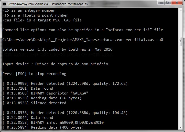
First tried to read the tapes on the real machine and save them on the SD card of my SDMapper, but I the success rate was low.
I tried to record the sound to decode on PC using one of the tools available (SofaCas, Castools) but the hum as quite high due to ground loop between the PC and the tape recorder.
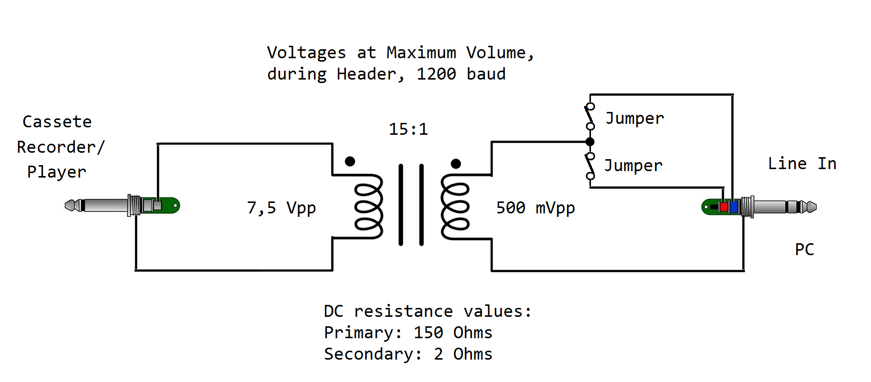
I looked all over my parts for a landline phone transformer with 1:1 without success. The best transformer that I could find was a transformer with 150 Ohms (measured with multimeter) at one of the windings and 2 ohms at the other salvaged from surplus PCBs.
I have tried out the transformer connected to the tape recorder at either side and measured the amplitude with the oscilloscope to determine the turns ratio.
After some measurements I did the math and found a turns ratio of 15:1. It is worth to mention that such figure will turn the 7.5Volts pk-pk produced by the cassette player can produce a voltage of hundreds of Volts at the secondary of the transformer, depending upon which side of the transformer the cassette is connected. When in doubt connect the cassette side to the transformer side with the highest DC resistance.
At the end this is how I have connected the transformer. I have used an stereo plug at the PC side because my sound card did not liked to have one of the channels short-circuited to ground. A couple of jumpers to allow me to select to record in any of the channels or in both at the same time.
I wish I had a transformer with smaller turns ratio, because the 500 mVpp produced were not enough to achieve full scale of the recording, but I could record and decode some programs.
Here are some screenshots of recording using audacity.
And a screenshot of SofaCas running
Some pictures of the device assembled.
A
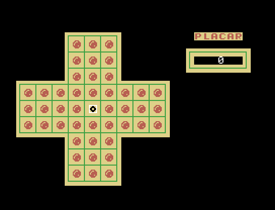
And a screenshot of one game that I have successfully recovered: "Resta 1" or Peg Solitaire.
For a matter of symmetry and sake of schematic drawing I have rearranged the wiring, so the MSX pin 8, a push-pull output became an open collector with pull-up resistor, then the pins/rows assignment became
ROW / (Keys)
MSX Joystick Pin
Keyb. Contr. Pin
0 / ( #, 9, 6, 3 )
8
6
1 / ( 0 , 8, 5, 2 )
6
9
2 / ( *, 7, 4, 1 )
7
5
Or in colors, lol!
I have also wrote a "driver" in assembly to perform some tests on an emulator. The code have been optimized in size the most that I could do and now it can read raw key scans from joystick ports 1 and 2.
; PSG IO addresses
PSGAD: EQU 0A0H
PSGWR: EQU 0A1H
PSGRD: EQU 0A2H


ORG 09000h
ld a,(PORTKB)
;
; Scan keyboard connected at Atari Joystick port
;
; Inputs:
;        register A: 0=Connector 1, >0=Connector 2.
ScanKB2600:
   and a ; set zero flag accordingly
   ; Save PSG Context
   ld a,15
   out (PSGAD),a
   in a,(PSGRD)
   ld (SAVPSG),a
   ld hl, KBROWS

   ; Select Joystick port accordingly
   jr NZ, ScanCon2

ScanCon1:
   and 10111111b  ; clear bit 6  (joy port 0)
   or  00010011b  ; set bits 4, 1, and 0  (all rows unset)
   ld b,a
   ld c,a
   res 4,a         ; row 0 (pin8) low, rows 1 and 2 (6 and 7) high
   res 0,b         ; row 1 (pin6) low, rows 0 and 2 (7 and 8) high
   res 1,c         ; row 2 (pin7) low, rows 0 and 1 (6 and 8) high
   jr ScanRow0

ScanCon2:
   or  01101100b  ; set bits 6, 5, 3, and 2  ( joy port 1, all rows unset)
   ld b,a
   ld c,a
   res 5,a         ; row 0 (pin8) low, rows 1 and 2 (6 and 7) high
   res 2,b         ; row 1 (pin6) low, rows 0 and 2 (7 and 8) high
   res 3,c         ; row 2 (pin7) low, rows 0 and 1 (6 and 8) high

ScanRow0:  ld e,a
   call SaveRow

ScanRow1:  ld e,b
   call SaveRow

ScanRow2:  ld e,c
   call SaveRow

RestorePSG:
   ld e,(hl) ; hl now points to SAVPSG

SaveRow:
   di
   ld a,15
   out (PSGAD),a
   ld a, e
   out (PSGWR),a   ; update register 15
   ld a,14
   out (PSGAD),a   ; select register 14
   in a,(PSGRD)    ; read keys hhhh*741
   or 11110000b   ; mask unused bits
   ld (HL),a   ; save keyboard state
   inc hl
   ei
   ret


; Variables

; keyboard rows hhhh#963, hhhh0852, hhhh*741
KBROWS: EQU 09800h

; PSG register 15 save state (overwritten at the exit)
SAVPSG: EQU 09803h

PORTKB  : EQU 09804h ; 0 -> connector 0, 255 -> connector 1
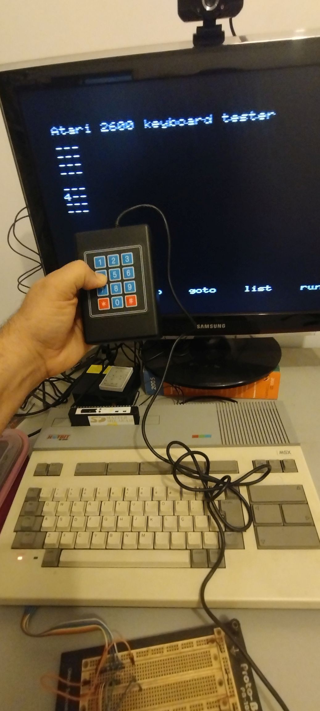
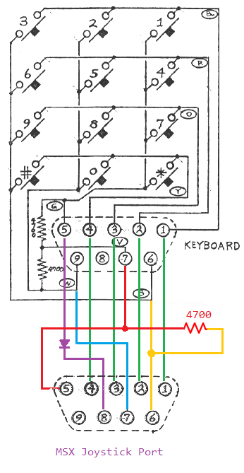
Following up a post from MSX Resource Center, I can think of an adapter to connect the Atari Keyboard Controller adapter on the MSX.
The keyboard can be read by pulling down consecutively the pins 6, 7, and 8 of the joystick port, while keeping the other pins at high, and read the key pressed on the directionals. A key pressed will appear as LOW.
The diode on pin 8 is to simulate an open collector thus preventing a combination of bad code an many keys pressed at the same time. The pins 6, and 7 are already open collectors and does not require the diode.
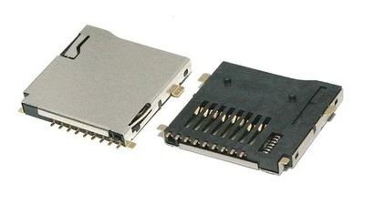
Should have started a project, lol but here we are with the last revision of the Single Sided PCB. now only one micro SD socket and two different adapters.
The model of micro SD socket looks like this
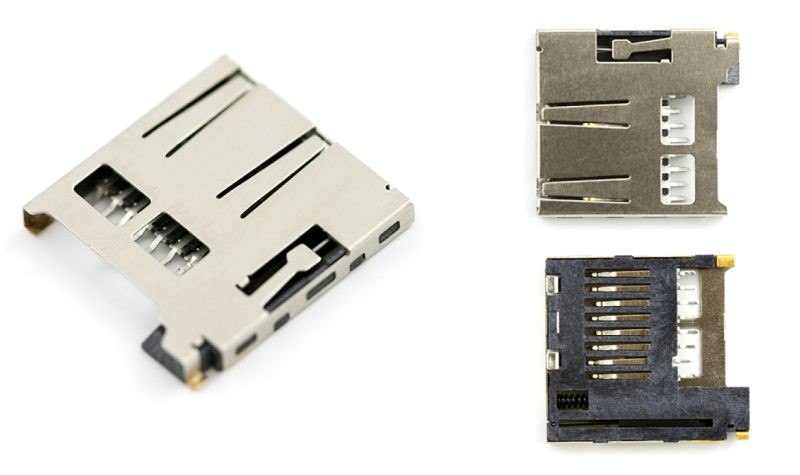
The micro SD socket adapter is usually shipped with the header pins out, hence it can be mounted facing up
The SD/MMC card adapter on the other hand is usually shipped with the pins assembles so it must be solded upside down.
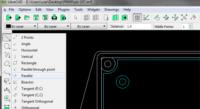
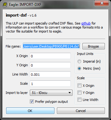
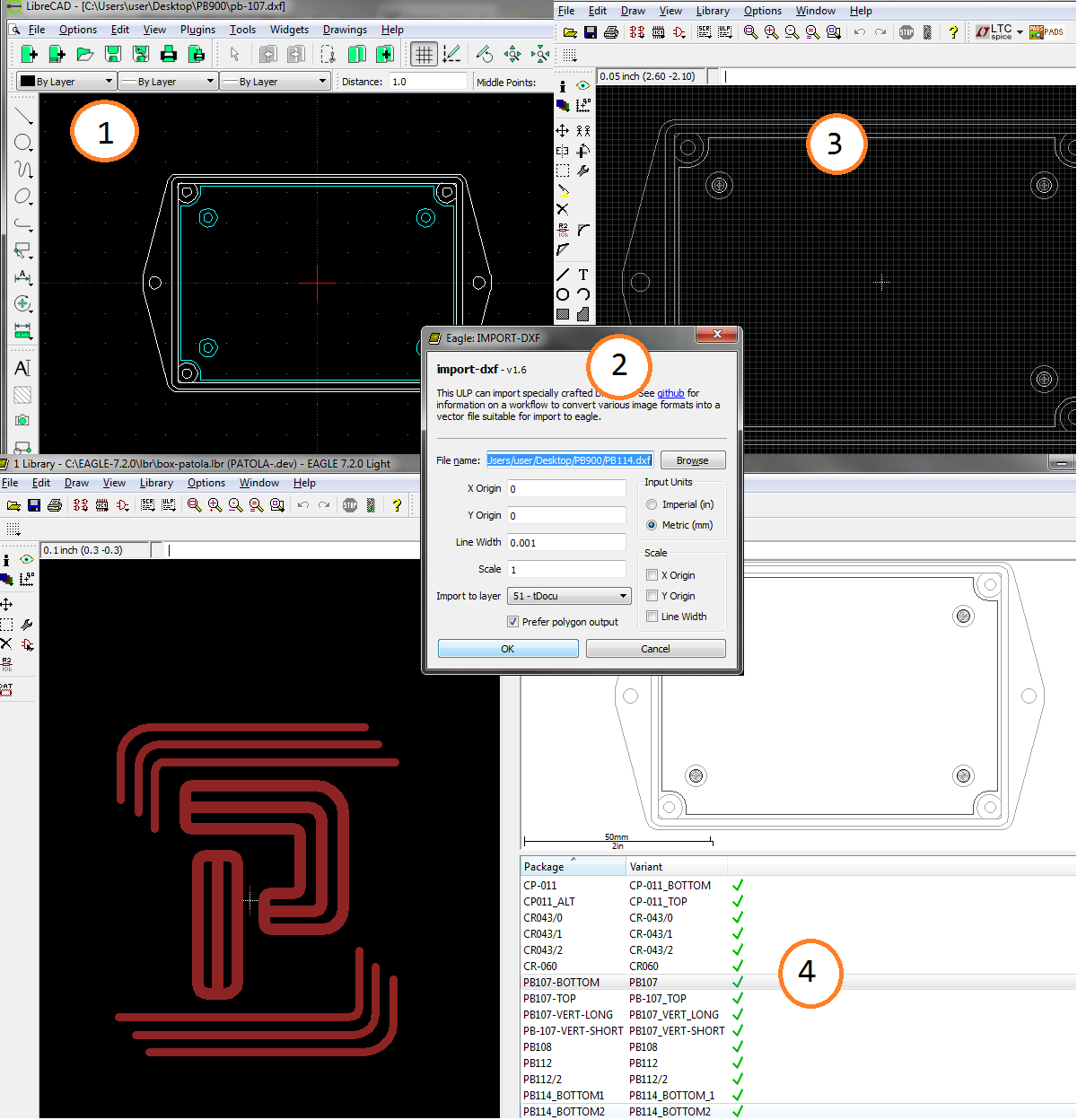
Most of the PCBs have been drawn using LibreCad and imported in Eagle using the import-dxf.ulp script.
The Case outline is drawn from the manufacturer's datasheets. Then I use the (draw) Parallel line and set the distance to 1 (mm) to draw the PCB outline around the external walls and standoffs and save the file as DXF 2007.
When I run the script I left the scale at 1, and use the same scale I have drawn (mm). As most of the details I have been drawing are on the case outline I choose the tDocu layer as a primary. I usually draw on more than one layer but the importing script merges them.
After loading the DXF I change manually the layers of the board outlines to the tDimension layer. The next step is to put some holes at the desired position.
Same procedure works fine for logotypes too, and it is very nice to trace the bitmaps from Inkscape and use them on eagle, though sometimes the Inkscape generated DXFs don't work.
I've been following athread on MSX.org to add recording functionality to Casduino. So far the tape reading is being done using sampling / signal processing but the real bottleneck seems to be the latency of the SD card writing.
Worth to notice that the same issue happens on the native playback function and such issue was worked around using an interrupt based playback engine.
Then I though why not use the same approach for the recording ?
I have started to work in the problem, and after reading the code on the BIOS listing altogether with the explanations on the Red Book, I came to an architecture using a state machine to mimic the behavior of some of the cassette routines.
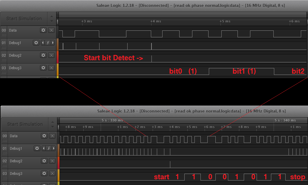
TAPION: Find a header in the cassette and measure the baud rate.
TAPIN: Read a byte from the cassette. Tape is read continuously until a start bit is found. Then read the next eight bits.
The resources used are one interrupt pin, programmed to trigger an interrupt at every pin change and the Timer 2 which runs free with a pre-scale set to advance one count at every 8us.
The _HEADER_SYNC state counts pairs of transitions until the difference between 1111 sequential pairs is within 32us (4 counts).
The _HEADER_AVERAGE state counts 512 single transitions to determine the average length of a full bit. The parameters LOWLIMIT and MAXBITLEN are defined as 25% around the average (MEDIA)
The _DATA_STARTBIT state add the time taken by sequential transitions until the sum is larger than LOWLIMT, which marks a transition from the last quarter cycle of a "1" bit to the first half of the "0" bit (the start bit). After that the second half of the Start Bit is read.
The _DATA_DATABITS was a tricky one to write (but not as tricky to make it work as the previous state). On the MSX the Z80 counts how many transitions occurred have passed within a given window of time to determine the state of the bit, whilst using interrupts, it is necessary to compare the time taken after you have 2 transitions. If it takes more than a LOWLIMIT, we have a bit 0 and we're happy. Otherwise it is necessary to wait to more cycles and we have a bit 1. After 8 bits, the data is pushed to the stack and the state return to _DATA_STARTBIT. As in real MSX the stop bits are ignored as they are there just to provide some time to process the data read.
Worth to mention that none of the interrupt routines do rely upon the phase of the cassete signal, but soleley on the timing between the transitions.
The _INTERRUPT state is there to take care of unforeseen conditions during the tape reading.
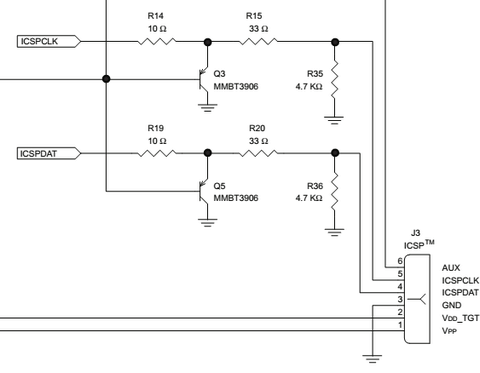
The PICkit2 programmer provides pull-down the PGC/PGD lines.
As such pull-downs may interfere in the circuit being developed, I have built a simple add-on for the PICKit2 that consists of a dual section switch that disconnects the PGD and PGC lines.
And I wish to use an audio generator to simulate such microphone. This can be accomplished by a voltage divider with the right resistor values.
Given the low voltage on the output as well as the low impedance, we could have a hunch that R2 should be very close to 9,5 ohms, but let's do some math. Note: Zout on my generator is predominantly resistive, hence I've added Z and R without further ado. Choosing 1V(RMS) for our source (that we can control anyway) and a Zi of 40 Ohms and solving the matrix we have:
No surprise here, but the math might be very useful to simulate other sources.
On the scope of this project I should use a 9,1 Ohm resistor (or even a 8,2 Ohm) for R2 and a 39KOhm for R1 and adjust my Vo to have .25mv on the output.
This week H-A-D featured an article with a home-built racing sim. While watching the video I have seen that the author did many connections on an Arduino board just inserting the wires on the pin header.
I have seen that before on a considerable amount of projects. It's not something I would rely on for a long term operation circuit, then I realized that there is room for a screw terminal shield. (Eagle Files):
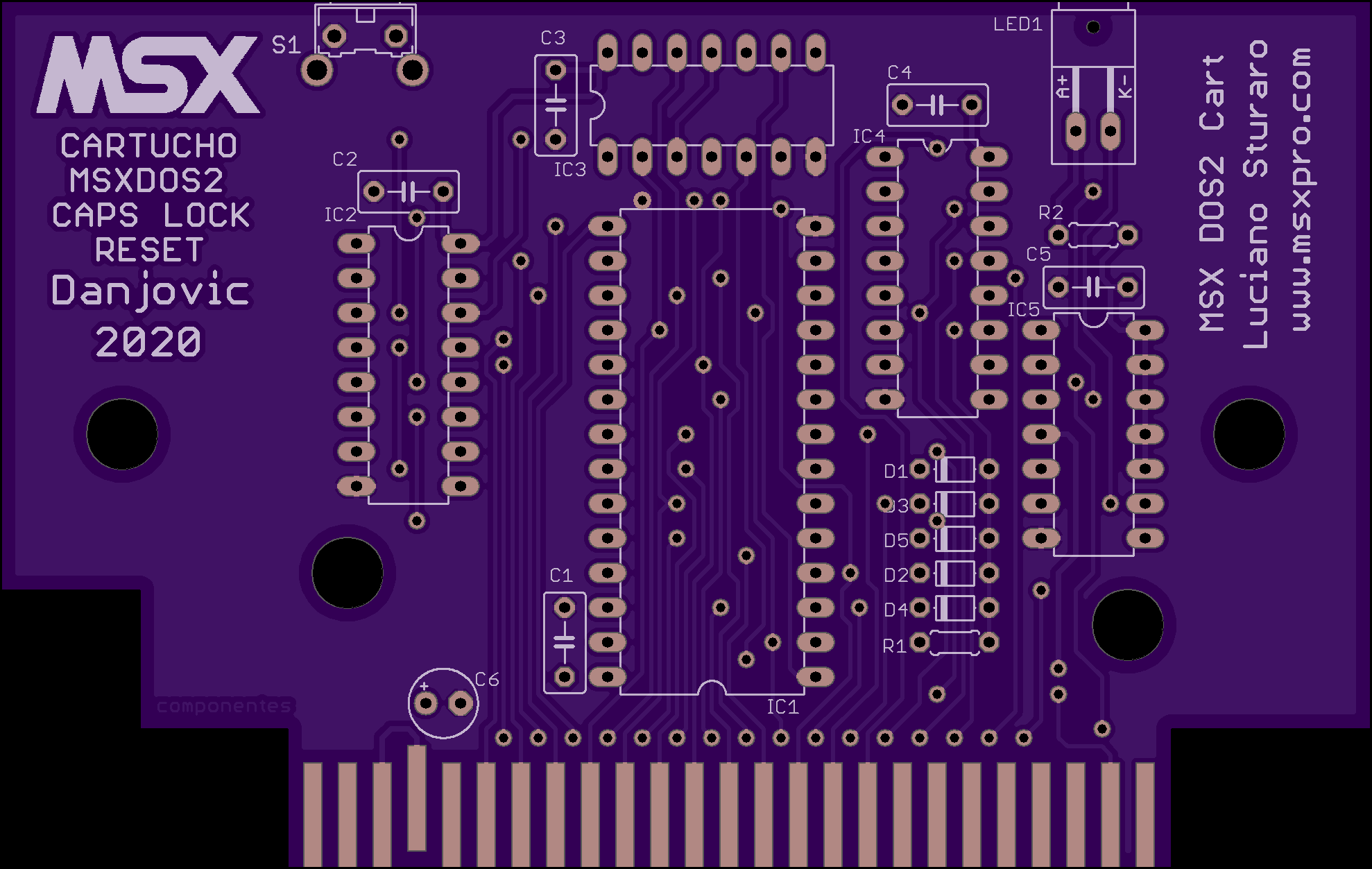
The Expert is a Brazilian manufactured in the 80's and it is compatible with MSX standard. It uses a detachable keyboard but it lacks the Caps Lock LED on the keyboard because the 13 pin connector used ran out of pins (even the shield is used as a 14th conductor for GND).
One day I heard about that issue on my favorite podcast, and just for fun I have designed a Caps Lock cartrige for the Expert. Some time later I have added another feature to the cartridge that is not implemented on the computer: a RESET button.
I have designed PCBs for the MSX cartriges before, like the MSXDOS2 cartride that contains a ROM with the MSXDOS2 kernel with some glue logic to perform the bankswitching (the circuit was not designed by me though). Such cartridge allows the Expert - an MSX1 machine - to run MSXDOS2 without a Memory Mapper.
On this sunday afternoon I have merged the two projects and created the Ultimate MSX Caps Lock cartridge:
The PCB and schematics files are available on Github. I have just routed the board, not assembled the circuit yet, sou use it at your own risk.
A 100% of the CD and DVD drives that I have from LG suffered from an annoying aging problem. After few months of use the CD/DVD fails to load the media and eject the disc. At first it occurs oftenly and gets worse with time up to the point the it fails everytime.
I needed to reinstall the operating sytstem on an old machine and the drive - an LG unit was at the point that it failed all the times.
Then I've took off the covers of the DVD player to figure out what was happenning and I have found that the loading mechanism required good force at the end of its course.
Such mechanism is driven by a belt that I found that was too loose - in the sense that it lacked tension - to provide the necessary friction.
To fix the problem I used a sillicone band torn in two (as it was too wide to fit). Though the perimeter of the sillicone band was much smaller than the original belt, it supported the tensioning very well and it restablished the DVD player.
Worth to mention that the belt can be replaced without openig the drive as the belt is reachable (using a tweezer) with the DVD with its door opened.
One of the participants of the MSX.org reported that the Digi:Arka worked very well with Arkanoid 1 but it did not worked with Arkanoid 2. One of the possibilities is that the rom might not have code to read the paddles, just like in the first title, and indeed it is possible to find two versions of the game with the differences pointing to corroborate this hypothesis:
But the user that reported me the problem have the original paddle controller that was bundled with the game and such controller works in both titles (Arkanoid I and II).
The idea for this project occurred to me while I was implementing the PC Joystick adapter for #Control Freak , and the user @Dave's Dev Lab mentioned that he had 300 IBM PC jr joysticks and I started to wonder if I could use the cheap Digispark instead of the Arduino Micro.
The PC jr joystick, as most of the early PC controllers provides only a couple of axes and two buttons. In other words only 4 I/Os are necessary and that is exactly what Digispark provides.
I could reuse some of the experience acquired during the development of support for paddles in the Atari adapter for my #AVeRCADE board, as long as I did some work to adapt the "raw" environment of V-USB+GCC to the Arduino "framework" used by Digispark.
First thing done was to synchronize the potentiometer reading to the USB interrupts. That can be achieved by putting the CPU to sleep(), and the timing loop will always run after the CPU wake up to service an interrupt. The header is required though.
Second thing to do is ti turn off Timer1. It took me some time to realize that the Timer 1 (instead of Timer 0) was generating unwanted interrupts, waking the micro controller at the wrong time. Some Arduino functions rely on this timer and therefore will not work, most notably the delay( )and therefore theDigispark.delay( ).
Main loop code:
voidloop() {
sleep_enable(); // Prepare CPU to sleep
power_timer1_disable(); // turn housekeeping off
sleep_cpu();
sleep_disable();
if (++interval > 3) { // run once in row of a three
interval = 0;
for (i = 0; i < 150; i++); // 100us delay
doNewSample();
populateValues();
DigiJoystick.update();
}
}
And the result:
Main loop continues right after the interrupts
As the USB interrupts occur 8 ms apart, it is easy to count how many times the CPU woke up and run the loop at the desired sample rate, but the least time interval that I could make it work was 1 out 3 which means 24ms.
The sampling loop was written to run as fast as possible. Inside the loop it is necessary to test if the capacitors have charged and each iteration must take exactly the same time. That was achieved without the use of assembly and the test is performed without the use of the "if" statement. The trick is simple: A variable is initialized at 0 (zero) and added to the state of the bit being tested at each iteration. It is necessary to invert the state of the input bits, though. While the capacitor is being charged and the voltage at its terminals is under the positive threshold voltage, reading the pin will result into Zero which inverted and mask will become 1 and the variable increments. After the voltage exceeds Vih, the variable will be added to 0 and will not increment anymore until the end of the counting cycle. Code is simple as that:
And the result is a counting loop of mere 300us (microseconds)!
The last piece of the puzzle is the calculation of the timing capacitor. The following parameters shall be considered: Charging time: ~310us Potentiometer Resistance for maximum charging time: 100k Ohms Supply Voltage (Vcc): 5Volts Input threshold voltage: Vih = 2.5Volts
The calculation formula is well known
The number crushing can be easily done with the aid of Wolfram Alpha
The closest capacitor value is 4.7nF
Buttons The only two pins left for the buttons are pin 1 and pin 5 and both will require some attention to make them work as button inputs. Refer to the diagram below:
On Digispark boards, digital Pin 1 is pulled down by a 1k Ohm resistor (R2) in series with an LED (D2). One option would be to rework the board and remove the LED or the resistor but another option, less invasive is to use a pull up resistor that provides a resulting voltage above Vih (2.5 as we have seen before) . Tests were performed with 1K and 560 Ohms resistors...
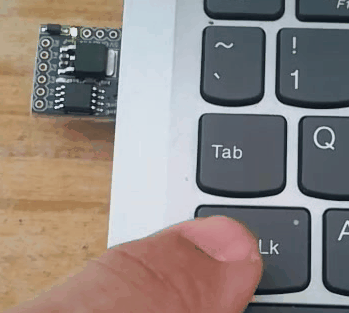
I have just added support for LED status on Digispark Keyboard library.
Now to get the LED status is just a matter of calling the function
DigiKeyboard.getLEDs()
DigiKeyboard.getLEDs()
and test for one of the 3 contants:
NUM_LOCK
CAPS_LOCK
SCROLL_LOCK
Just like in the example
// USB Caps Lock Led gizmo - Danjovic 2020
// Use modified version of DigiKeyboard library// https://github.com/Danjovic/DigistumpArduino/tree/master/digistump-avr/libraries/DigisparkKeyboard#include"DigiKeyboard.h"voidsetup(){
pinMode(1,OUTPUT); // Digistump BuiltIn LED as output
}
voidloop(){
// Check the state of Caps Lock and change led accordinglyif (DigiKeyboard.getLEDs() & CAPS_LOCK)
digitalWrite(1, HIGH);
else
digitalWrite(1, LOW);
DigiKeyboard.delay(10);
}
The modified version of the libraries are available at:
This is another method for providing analog position to Atari 5200 that does not depend upon internal calibration.
The analog controller information is measured by Pokey chip that measures the time a capacitor takes to increase its voltage from near zero to a given value. This time varies with the resistance of the potentiometer axis.
Many videogames and computers, like ATari 2600, PC gameport, Apple][ gameport usually discharges the capacitors right before start a new reading cycle. On these systems is just a matter of waiting for the capacitors to discharge to know when to push the line high to provide a desired position (timing) information.
But in Atari 5200 that is not so easy because Pokey chip keeps the capacitors discharged by until the next sampling cycle that depends upon the game loo, therefore the discharge moment can not be used as a time reference.
The experiments that I have done consisted in:
polarize one of the pot inputs with a resistor that provides a low counting, e.g. 10KOhms and detect the voltage increase before it reaches ~1.9V that is the input threshold voltage of POT pins in Pokey Chip.
Then the line is forced LOW by the time enough to provide the desired counting in Pokey chip.
Finally the line is pushed high to exceed the threshold voltage and that makes pokey capture the exact counting.
Worth to mention that this method does not depend upon internal calibration of Vac voltage (at pin 9).
The links [1][2] are for two videos with the first experiments. The tests have been performed on a AVR (Arduino board) together with the #Atari 5200 Controller Port Emulator
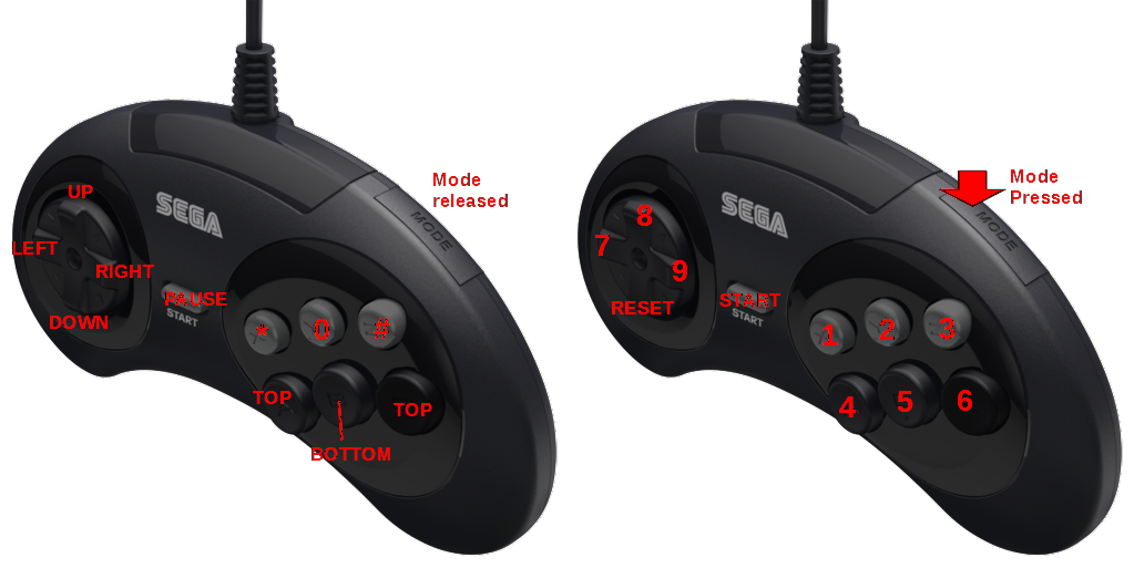
MegaPlay adapter lets you play Atari 5200 using a 6 button Sega Genesis controller yet providing full keypad control.
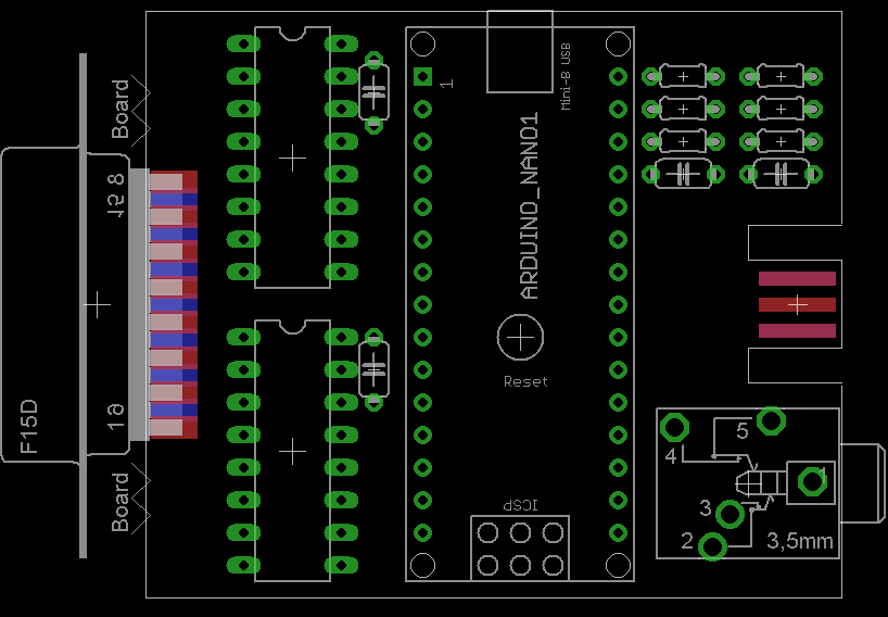
The circuit can be built using an Arduino Nano and two analog multiplexers. Interface with analog joystick can be borrowed from "Low Priced MasterPlay clone adapter".
Keypad presses can be emulated by activating a pair of analog multiplexers. This scheme allow the simulation of 1 (one) keypress at a time, but frees the software from critical timing.
The Atari 5200 controllers are well known by its low reliability. Many alternatives to the original controllers have rose along the time from when the sytem was being sold on stores up to present days when it is possible to find adapters being produced and sold by members of Atari Age community forums. The adapters found today can be either:
a) analog - based on digital potentiometers or
b) digital - based on switched resistors.
Both change resistance in a RC network that is used by the console to convert a time measurement into positional information.
There are other ways to do it, though:
Applying a variable voltage on a fixed resistor. The charging time depends upon the RC constant for a given potential difference (voltage). That is pretty much how the trackball works.
Detecting the moment the timing capacitor start to charge and hold the voltage low until the correct timing has passed. On the 5200 it is a tricky task, because the capacitors do not receive a pulse (of known time) to discharge. Instead they are held discharged until the CPU generates a pulse internally that releases the charge.
I have figured out the methods above after went through plenty of technical information such as datasheets, books and forum posts. In the meantime I have worked on the design of some alternative controller adapters:
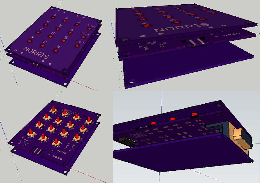
Norris: Adapater for Wii Nunchuck controller.
Provides vertical/horizontal movement plus 2 buttons. - Keypad functions are provided by tactile switches. - Body composed by 3 PCBs stacked on top of each other
Built-in Wii Nunchuck connector on PCB
Wire bridges on PCB to hold game faceplates
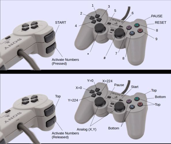
Hunter: Adapter for Playstation Dualshock controller.
Provides vertical/horizontal movement plus 2 buttons - Analog sticks can work together or expand to a second connector (for Robotron)
Directional D-PADs work behave like digital controller on Masterplay adapter
Numeric Pad emulated by the controller by pressing L2. Worth to mention that emulating the keyboard can be somewhaty tricky too.
Can emulate behavior of trackball, behaving like the Trackpoint on Thinkpads
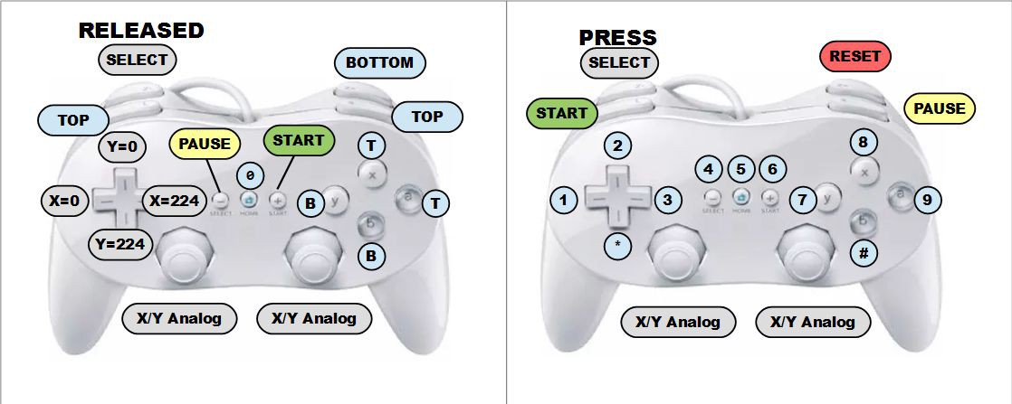
Stingray: Adapter for Wii Nunchuck Classic controller
Basically the same functionality of the Hunter
Numeric Pad emulated by the controller by pressing ZL
Built-in Wii Nunchuck connector on PCB
Concept board for StingRay
Second controller (for dual stick games) is connected through P2 Jack. If necessary GND connection wire can be used for one of the triggers of the second controller.
So far the controller adapters I have seen for the Atari 5200 and that can provide analog control use a used a digital potentiomenter (and extra capacitance).
This is certainly a nice solution but there are other alternatives, though:
1) Keep series resistor constant, vary the voltage applied to charge the capactor (just like the trackball do)
That can be done with a PWM providing 0-5V and some resistors in a network to match the desired voltage range. This method is used on the CX-53 trackball.
2) Detect when capacitors start to charge and hold the line down until the desired count, then push the line to +5V
It is a pity that the architecture of the Pokey Chip, used by the Atarti 5200 to read the potentiometers do not discharge the capacitors at the beginning of the sampling cycle but at the end. The only mark of the beginning of the charge is that the voltage over the capacitor starts to ramp up and that can be done by the analog comparator of a microcontroller set to a voltage that is below the minimum Vih (1.9V). Luckly there is plenty of time to react to that, as the pokey counts in Hsync lines (64us ).
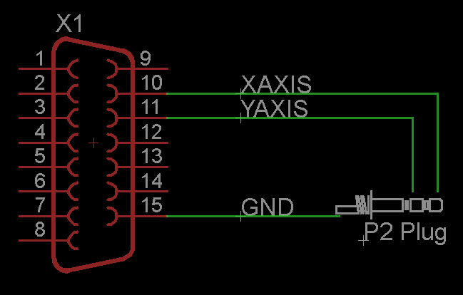
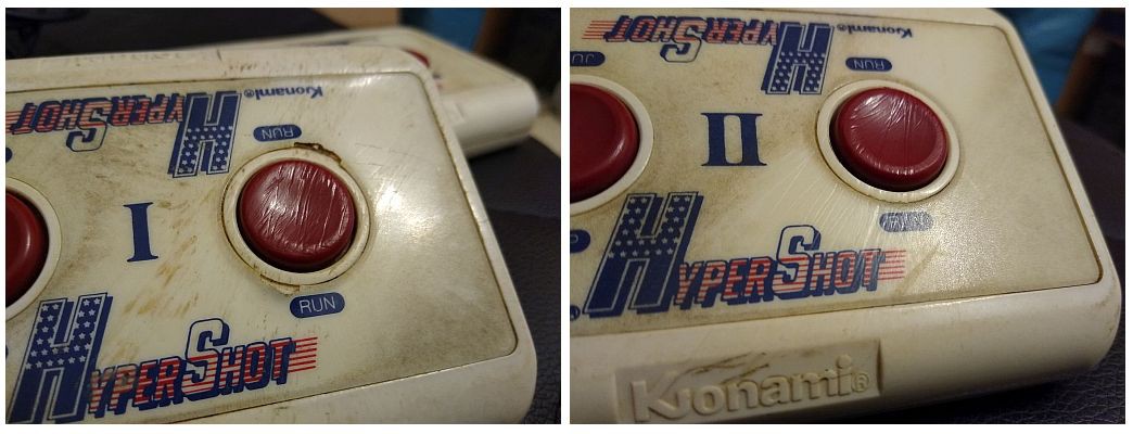
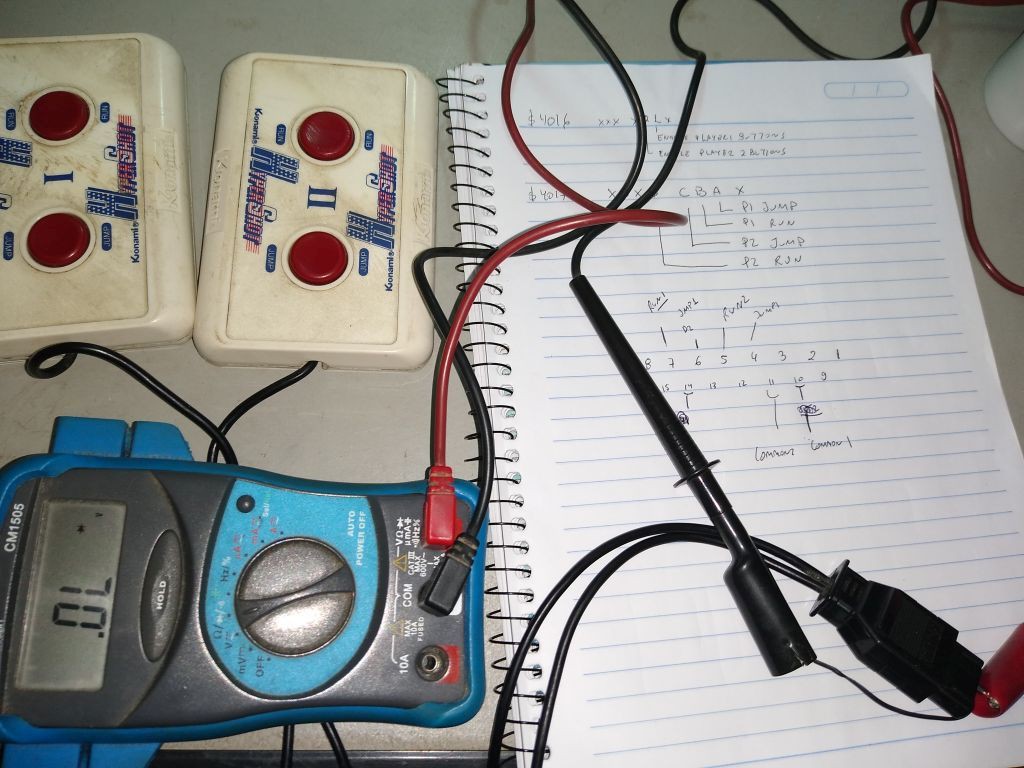
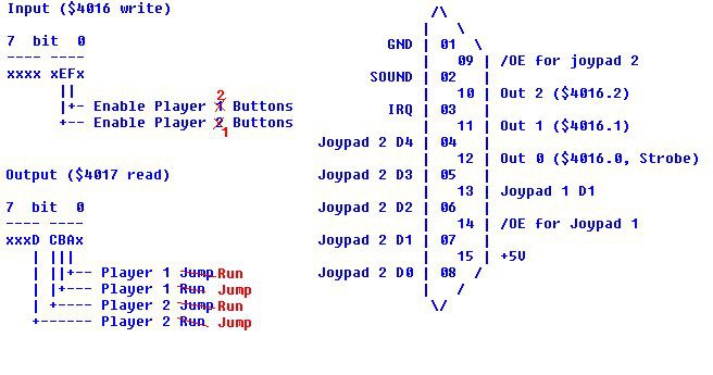
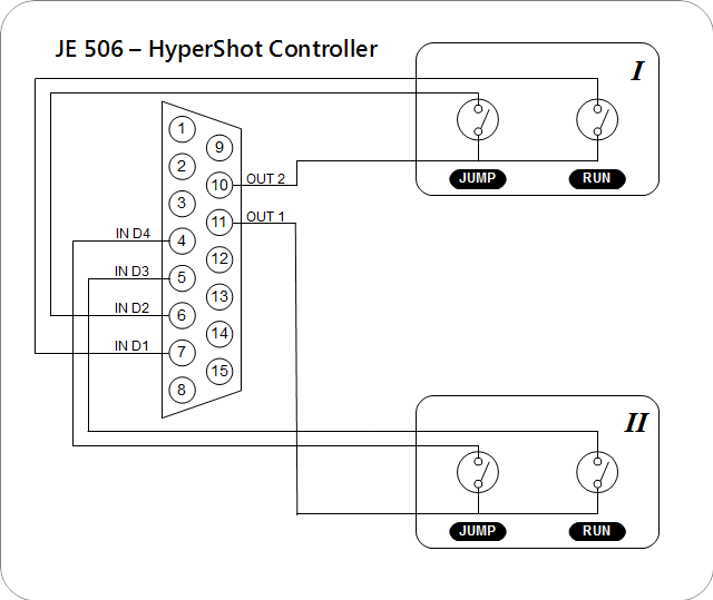
I have acquired recently a Hypershot controller for Famicon model JE506. Such controller comes in a pair and share the DB-15 connector to be attached on expansion port.
Given the state of the buttons I wonder if the previous owners were Wolverine and Sabertooth...
Nevertheless I got some reading on NesDev Wiki that pointed that the Hypershot controllers should be read by the console as single switches instead of a stream of data. Such information were confirmed with a multimeter.
The measurements performed were compared with the information presented on the wiki about the JE506 controller. The results show some difference from the JE506 information presented elsewhere on the wiki, considering the pinout of the expansion port presented elsewhere on the wiki. The Common pins for controllers (Out 1 and Out 2) are exchanged, as well as the JUMP/RUN function for both controllers.
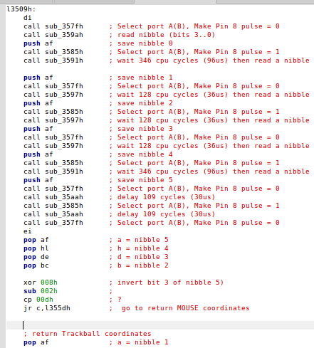
After spent some time unsuccessfully looking for precise information about the Mouse protocol used by MSX computers I got a subrom binary to disassemble and take a look.
Mouse reading is performed by NEWPAD subroutine at address 0x1ad but the reading effectively occurs after addres 0x3509:
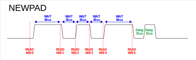
The Mouse routine reads 6 nibbles (0..5) in sequence, cadenced by the (toggling of) pin 8. Small delay loops are inserted between readings. Both the Mouse and the Trackball reset their internal counters after one edge of the Pulse signal.
The 5h nibble read might be the High order nibble for the Mouse or the delta Y value for a trackball.
Given the typical DPI resolution of the MSX mouse no displacement above 16 steps should be observed, then the expected value for the 5th nibble should be 0b0000 for positive displacement or 0b1111 for negative displacement.
The trackball is a much less resolution device and uses solely 4 bits, nevertheless as the mouse only a small amount of displacement should be observed (zero or one count up/down).
One of the curious aspects of the trackball is that it uses an inverted sign bit, which means "0" displacement is represented by 0b1000, and that is the key for the NEWPAD routine to differentiate a trackball from a mouse.
; Nibble 5:  Trackball: Delta Y, inverted Sign bit
;            (7) 0111  (-1) minus one
;            (8) 1000  ( 0) zero
;            (9) 1001  (+1) one plus
;
;            Mouse: Delta X high nibble, normal sign bit
;            ( 0) 0000  ( 0) Zero
;            (15) 1111  (-1) Minus one

xor 08h    ; Turn values 7, 8, 9 into 15, 0 and 1
sub 02h    ; Turn 15, 0 and 1 into 13, 14 and 15
cp 0dh     ; Trackball should greater or equal 13
jr c,returnMouse ; values less than 13
;
returnTrackBall:
....
The brief positive pulse issued after the 6th nibble is read has the purpose of reset the internal Y counter of a mouse, as registers should be read in pairs (4 nibbles).
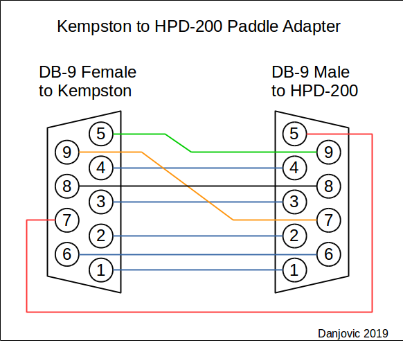
Sinclai ZX computers (ZX81/Spectrum) don't ship with a joystick port but they can count on the ubiquitous Kempston interface to provide 4 directional lines plus 3 buttons and that is more than enough to connect a Sega Master System HPD-200 paddle controller.
Paddle detection and reading code provided by SMS POWER. I/O address changed to match Kempston (0x1F), though.
A simple hardware adapter is necessary in between the Kempston interface and the HPD-200 paddle
An alternative for the HPD-200 is to build a DIY SMS/MarkIII paddle controller by Raphaël Assénat. In such case the wiring can be modified to route the signals from pins 5,7 and 9 thus dispensing the use of the adapter.
Example code (work still in progress) available at my github repository.
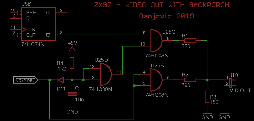
I believe it is possible to add a backporch for ZX97 (original) using three available gates from U25.
D11 discharges the capacitor at each negative horizontal pulse coming from /CSYNC and causes pin 11 of IC25 to go LOW, which blanks the video output signal at U25C.
After the sync pulse leaves R4 start to charge the capacitor. While the voltage is below positive threshold of U25 inputs the video stays blank, thus generating the backporch level. After that the output of U25D goes HIGH and the video content coming from U5B pin 8 can reach the output.
It might be necessary to fiddle with the value of R24 according with the technology of U25 (LS, HC, HCT, etc)
The resistors R1,R2,R3 were calculated to provide full compatibility with RS170: 1Vpp @ 75 Ohms load, 70% Video, 30% sync, DC coupling at output (the latter is a de facto standard).
This circuit have not been tested yet on the ZX97 but works like a charm on TK85 (a ZX81 clone)
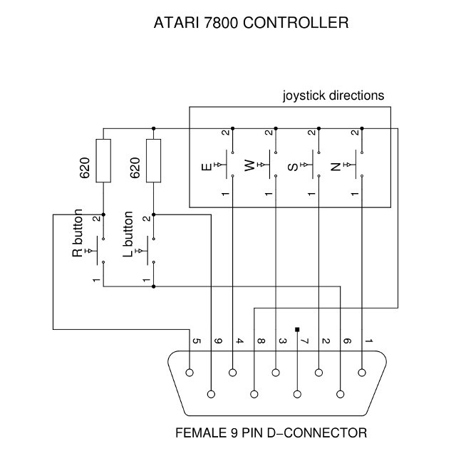
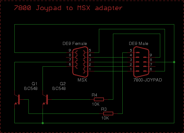
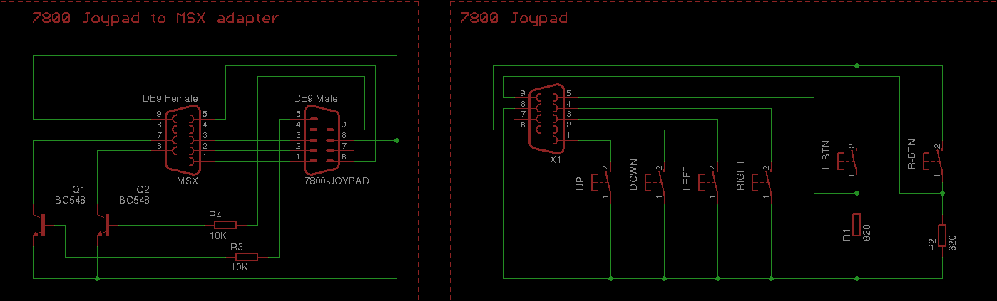
One of the users at msx.org tech forums asked if was possible to use Atari 7800 joypads in MSX.
The 7800 controllers are very similar to 2600 and therefore to MSX. The main difference is that to maintain compatibility with 2600 joysticks whilst providing two buttons, the 7800 used active high buttons on pins 5 and 9 which are used in 2600 for paddle inputs.
The straightforward solution is to invert the signals and that can be accomplished by a pair of NPN transistors.
Controller and adapter schematics, side by side, for better understanding.
My version of PCB for "SD2IEC Revisited" from Retrohax (https://www.retrohax.net/sd2iec-revisited/). Hand routed, has basically the same dimensions and can be even built by tone transfer (no vias under components).
Board shared at OSHPARK (link) and at Github (link)
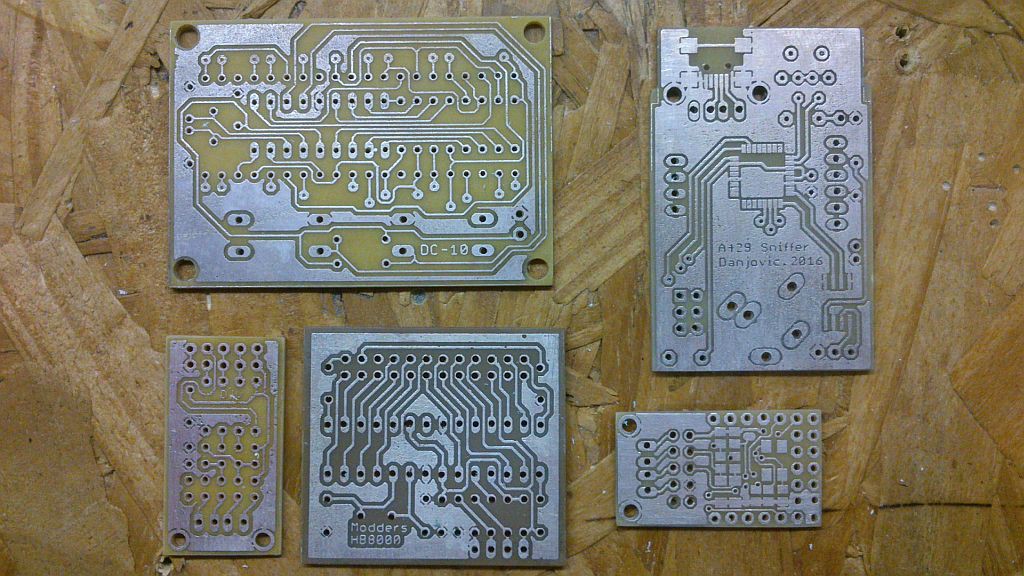
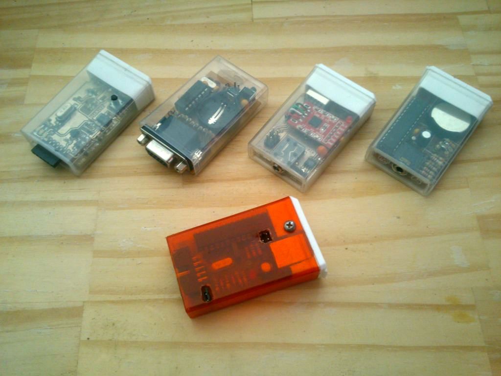
My collection of homemade projects stuffed inside Tic Tac boxes.
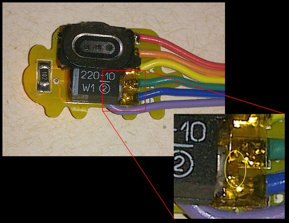
From left to right: Pickit2 clone, USBAsp, TicTacX, Arinc429 Sniffer, 32 Shades of GreyPICKit2 cloneUSBAsp Tic Tac XArinc 429 sniffer/analyzer32 Shades of GreyAnother view of the collection
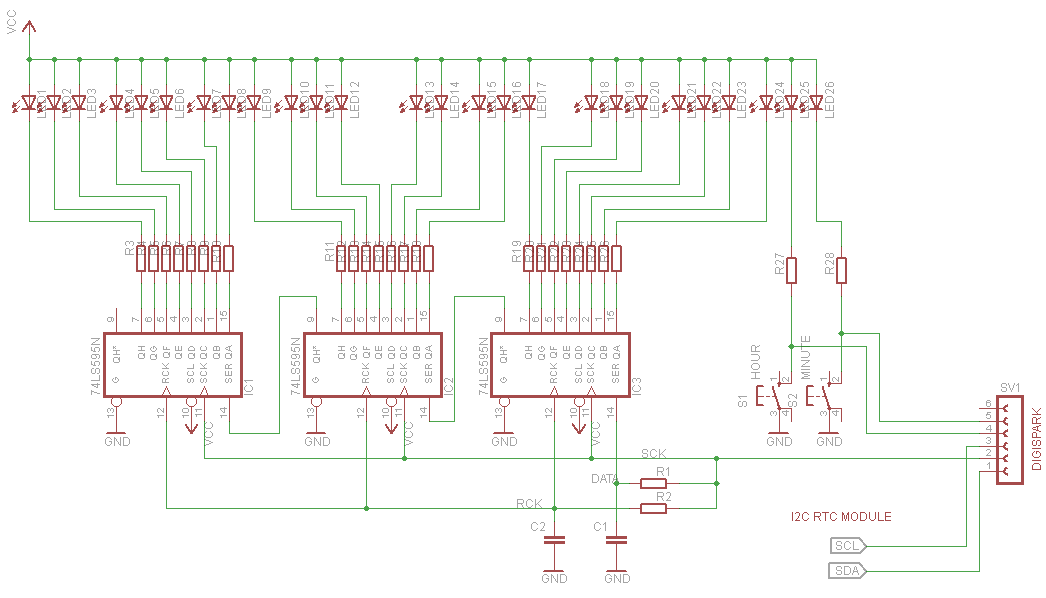
Inspired by #Linear RGB LED Clockby Jan I decided to build my version. Instead of RGB LED addressable strip I'll be using regular LEDs and shift registers.
As I am planning to use the cheap chinese Digispark boards and a minimal of components. Since RESET pin is not available as I/O in most of the cheap boards I have only 5 pins to spare.
Two pins are for I2C communication with the RTC module
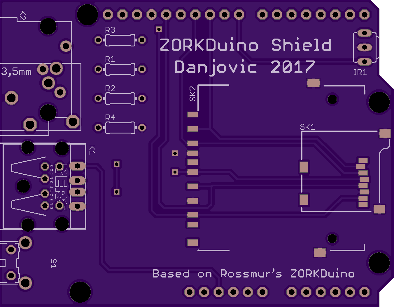
Browsing had.io pages I've stepped on the amazing #Zorkduino project wich implements a Z-Machine to play text adventure games (like Zork!).
The original project is very cool but it was build upon some ready made modules and a proto-board, so I've decided to route an specific board for the project named ZorkShield.
The board was designed to allow the assembly of both SD or MicroSD card slots and also allow the assembly of either a P2 stereo jack or a dual stacked RCA female for audio and video.
The video output have been slightly modified so the voltage and output impedance follow the RS-170 standard (like #VGA Blinking Lights). As a late time improvement I've added a RESET button.
Despite the board is a double layer It can be etched at home using tone transfer.
The layout was uploaded to OSHPARK but soon I'll upload it to github.
Today I have received a Microchip news with AVRs on it. That's the first time I ever seen Microchip advertising AVR microcontrollers. Despite the acquisition of ATMEL by Microchip is old news now this ad still blows my mind, lol!!!
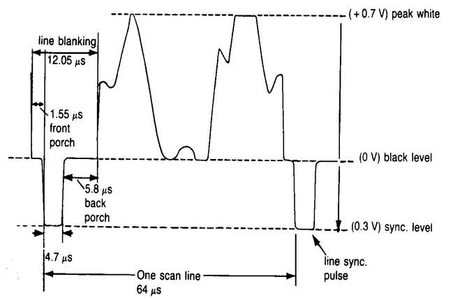
Composite video standard defines a signal with 1Vpp amplitude under a 75 Ohms. From that signal 70% (0.7V) is the amplitude of video information which stands above a 0.3V pedestal, while the synchronism information (sync tip) corresponds to the remaining 30% of the total amplitude or 0.3Volts below the pedestal.
Many projects of video
generation for microcontrollers provide video signals that may work
but don't respect the video standard, thus the signal generated might
not be properly displayed depending upon the monitor used.
But generating a video signal with correct amplitude and impedance can be easily accomplished with the aid of resistors and some math.
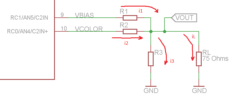
Consider the circuit topology below where pin named VBIAS generates Sync signals, while VCOLOR pin generates video signals.
With two pins for
generating the Sync and Video information we can have four possible
combinations from which only three are expected: Sync level, Black
(pedestal) and White Level.
We need then to
calculate the value of the resistors wich can provide the following
voltages
Black Level    0.3 Volt @ 75 Ohms
White Level    1.0 Volt @ 75 Ohms
Sync Level       0 Volt @ 75 Ohms
First thing to consider
are the Voh and Vol from the microcontroller. Taking a PIC16F688 as
example such levels can be in the range from VDD-0.7Volts to Voh and
0.6Volts to Vol. It means that our Sync level might be slightly
biased to 0,3Volts under 75 Ohms load (0.6Volts without load).
Our amplitudes must
then be corrected to compensate for the biased Sync level while
maintaining the total amplitude in 1Vpp
Black Level    0.6 Volt @ 75 Ohms
White Level    1.3 Volt @ 75 Ohms
Sync Level      0.3 Volt @ 75 Ohms
Considering the
resulting internal impedance of 75 ohms such values shall be doubled
when no load is present.
Now we have the
necessary information to calculate the resistors. Let us use
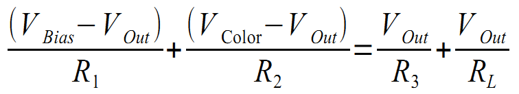
Kirchoff's current law: “At any node (junction) in an electrical
circuit, the sum of currents flowing into that node is equal to the
sum of currents flowing out of that node”
Then we have
Considering the
voltages involved we have now the generic circuit equation:
Let us use Conductance
instead of Resistance to make the math easier to deal with
Then for RL=75Ohms,
VOL=0,6Volts e VOH=4,7Volts (PIC Vdd @ 5,4Volts) the equation for
the three possible video levels are:
On the absence of load,
RL = infinity, which means the Conductance is zero. Then we have the
equations for the unloaded circuit.
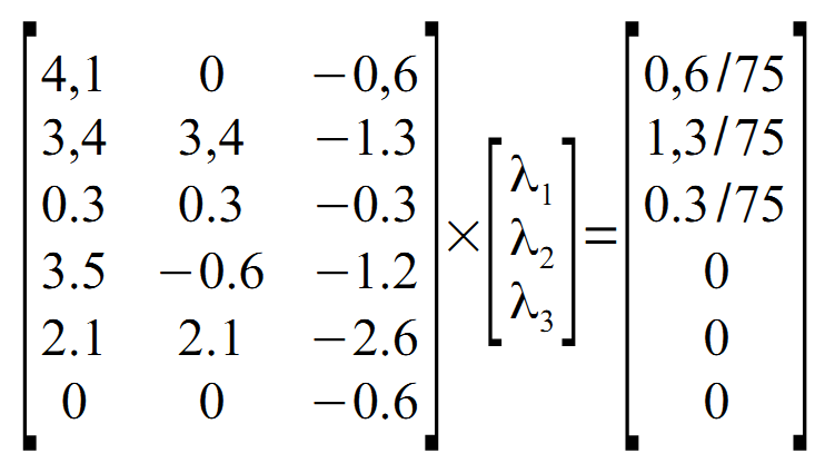
The 6 equations can be
written as a product of matrices
Using Scilab we can
easilly get the resulting conductances.
Which can be converted
to resistances, resulting in
>x.^-1
Then using the most close
commercial values we have:
Let's now do the
oposite way and check which are the theoretical values we can achieve
using commercial value resistors. Rewriting the equations in terms of
Vout we have:
Then solving for the
possible output levels we have:
Level   Vsync  Vvideo  V Out(@75R)  V Out (no load)
Black    4,7    0,6       0,64         1,29
White    4,7    4,7       1,35         2,71
Sync     0,6    0,6       0,17         0,35
Let us now estimate the
output impedance by the ratio of voltages with and without the 75
Ohms load.
Vopen/Vload = 2,71/1,35 = 2,01
Then from Thèvenin:
In plain numbers we
have ri=75 * (1,01) = 75,75 Ohms. Good enough!
The figure below shows
the circuit with final values.
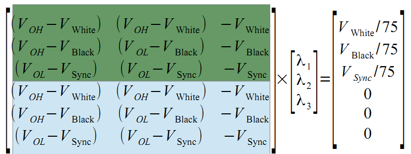
For calculating the resistor values for other microcontrollers and logic gates (TTL, CMOS) it is possible to use the general matrix system below. The green lines correspond to the voltage levels with 75Ohms load while the blue lines are the voltages with open circuit (no load).
In Scilab, it is possible to use the equations below:
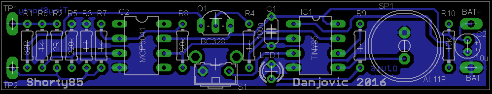
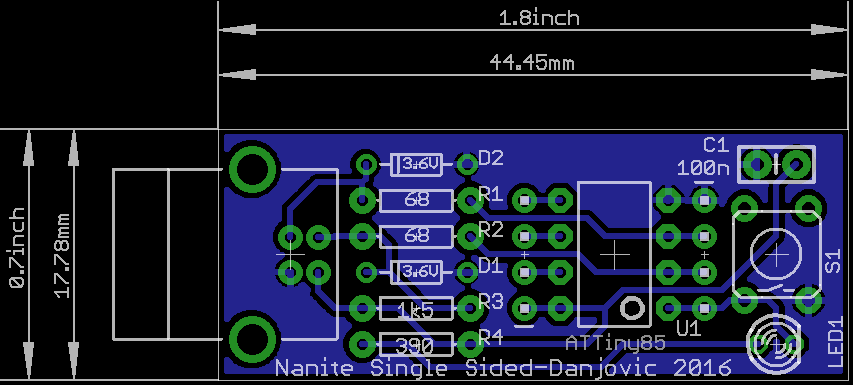
Following a suggestion from [tekkieneet] to rotate the microcontroller 90 degrees and move the push-button to the right edge of the board I have redesigned the layout this time also using Kicad.
I've posted a remark on the article "Creating a PCB in Everything" endorsing the design of single sided PCBs for DIY projects since they are far easier to replicate at home using techniques like toner transfer.
I've then started from original Nanite board and designed a single sided board for it, tinier as possible, using only PTH components.
By using our website and services, you expressly agree to the placement of our performance, functionality, and advertising cookies.
Learn More


 As such pull-downs may interfere in the circuit being developed, I have built a simple add-on for the PICKit2 that consists of a dual section switch that disconnects the PGD and PGC lines.
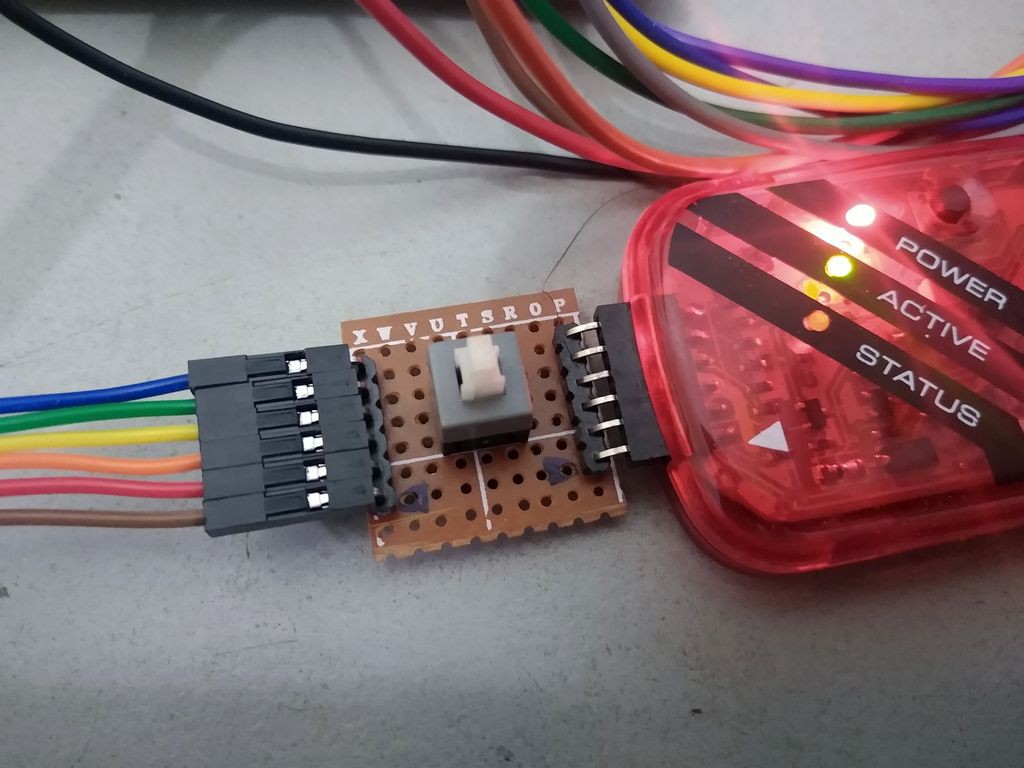

 Given the low voltage on the output as well as the low impedance, we could have a hunch that R2 should be very close to 9,5 ohms, but let's do some math.
 Note: Zout on my generator is predominantly resistive, hence I've added Z and R without further ado.
 No surprise here, but the math might be very useful to simulate other sources.
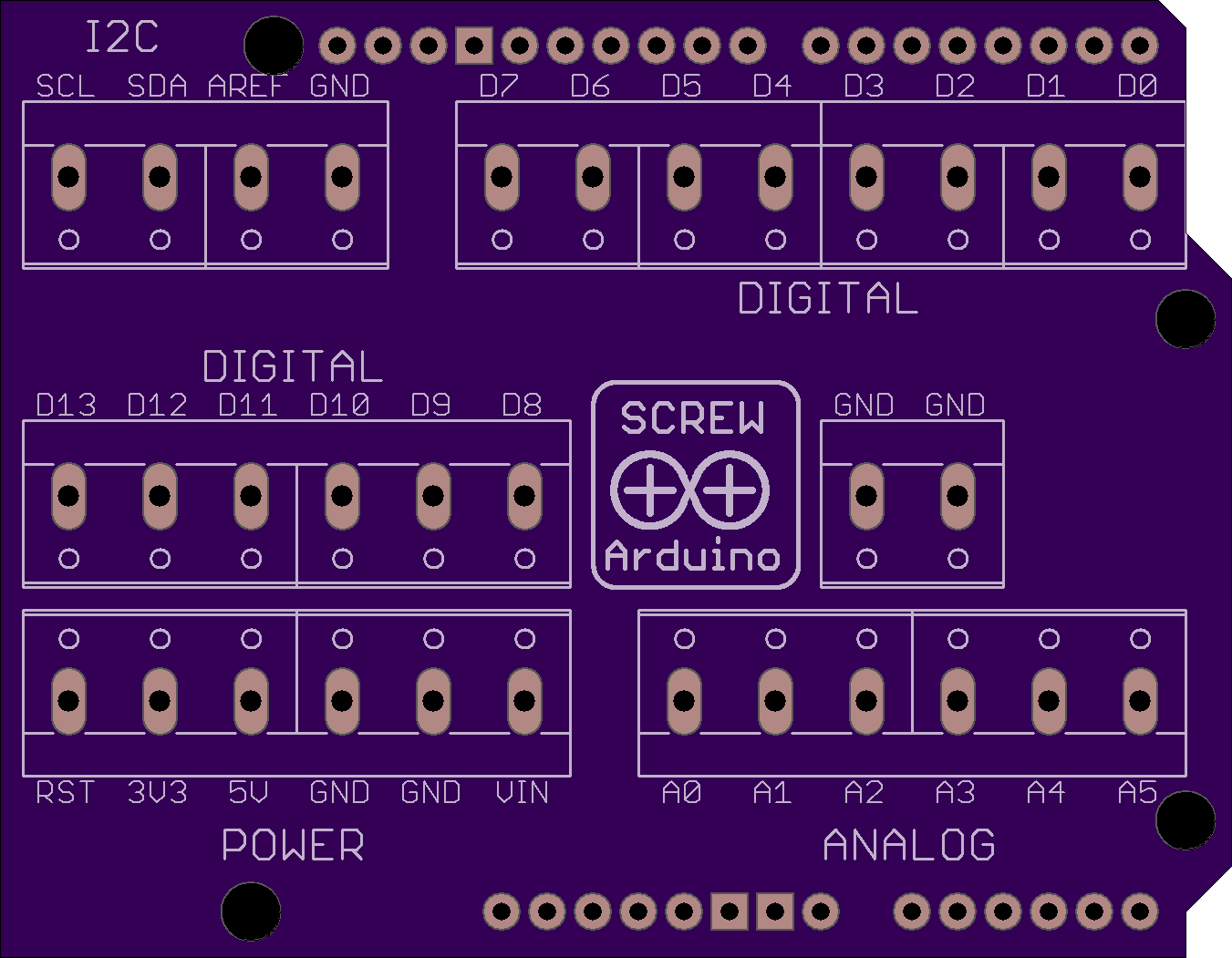


