Close
0%
0%

Semiconductors @ Home

Building all the tools neccesary to make chips at home.

Public Chat
Similar projects worth following
I want to make chips, period.
In order to do that, I have to build specialized tools to be able to do so.

1.- Vacuum chamber for DC sputtering deposition. (completed)
2.- HVAC manipulator with glass feedthrough (completed).
3.- 1200ºC tubular oven with integrated timer. (completed)
4.- Spin coater (completed, missing proper buttons)
5.- Hot plate. (completed, requires housing)
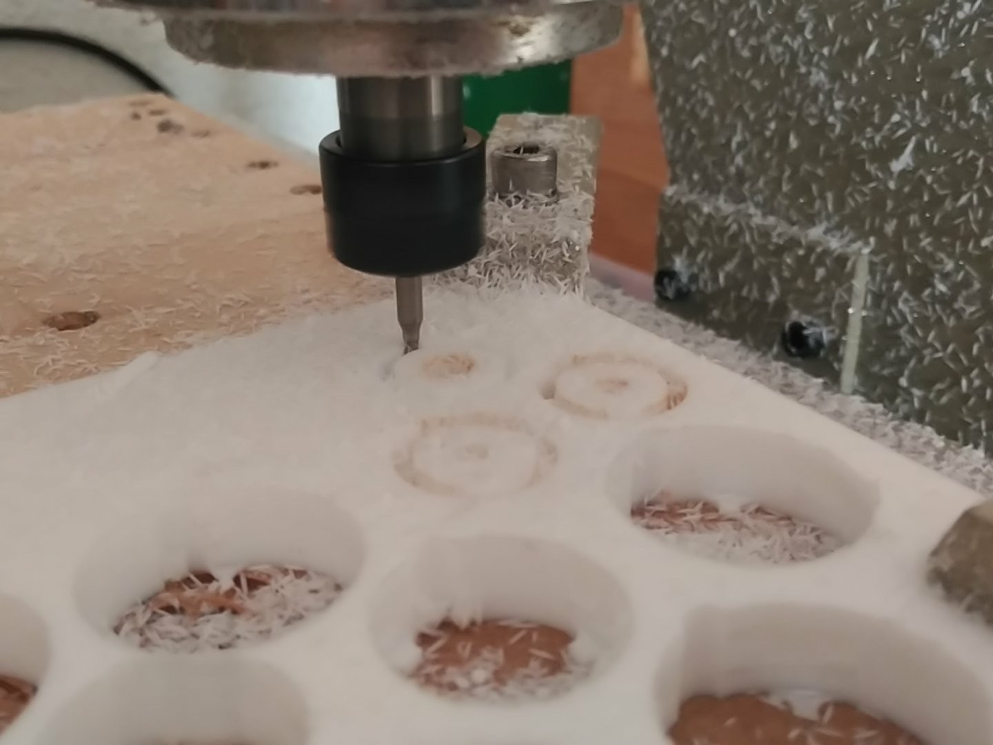
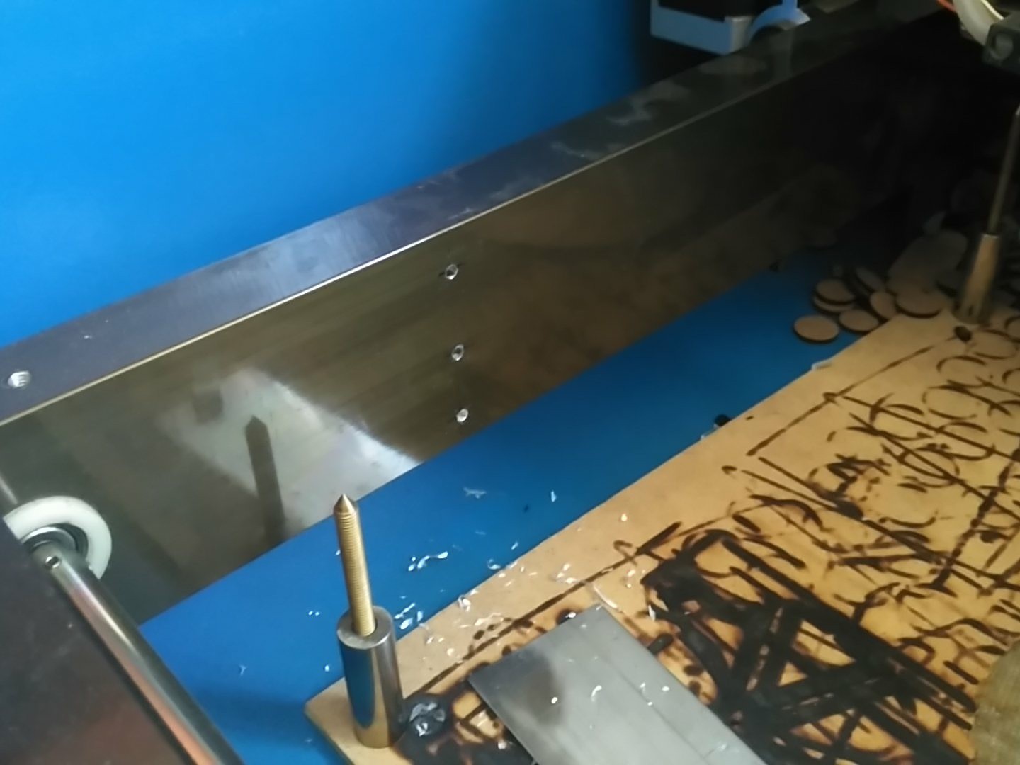
6.- Laser milling of PMMA in Silicon for first tests and 100µm feature size (completed)
6a.- Micro focus adjuster (completed).
6b.- Adding a camera for fiducial location (completed).
7.- Fume hood (completed)

Special Thanks to Niklas Fauth (https://hackaday.io/niklasf) for his invaluable help sourcing future testing hardware and other tools for future research.

To build semiconductors at home, you need a 1000ºC oven with controlled atmosphere, a way to diposit metal on top of silicon and a safe way to handle deadly acids. There are also complementary tools, like a spin coater or a hot plate, needed to apply acid resistant film on top of the silicon, to etch away the patterns.

All that can be made at home with some ingenuity.

Two pdf "Books" have been created from all the research done for this project. (stored in the "Files" section.

  • Semiconductors @ Home - Compendium! (all knowledge on the tools required for each process, the main focus of this project)
  • Semiconductors @ Home - Cookbook!      (a step by step guide to use the tools fabricated, under constant update)

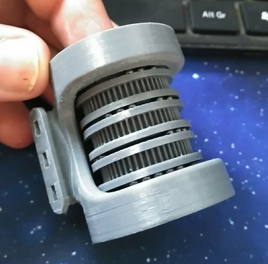
Below, some image highlights of the different tools and processes:
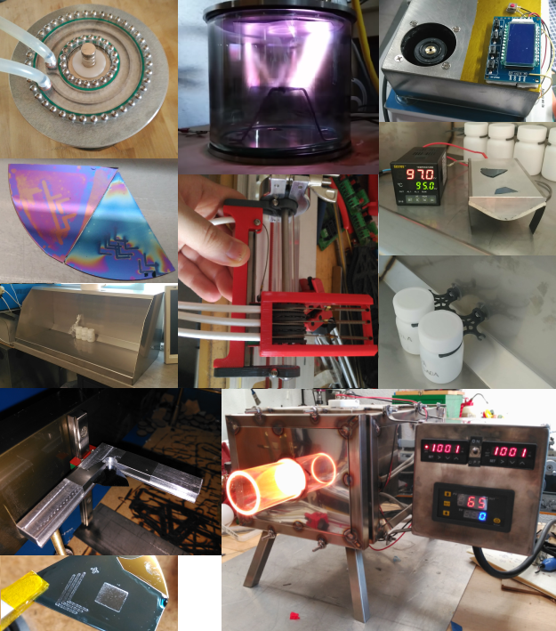
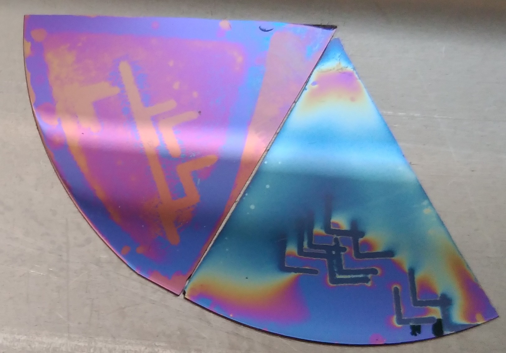
First diode, using Boron acid dopant in N-type silicon (phosporous):

For smaller resolutions, the plan is to investigate UV-curing resins and DiY e-beam maskless litography on PMMA, repurposing a CRT tube with a custom controller (already in prototype stage)

Once the semiconductor process is refined, vacuum wirebonding and DiY chip carriers will be tested.

Semiconductors @ Home - Compendium V.005.pdf

The knowledge book to understand how to build all the DiY equipement needed to make semiconductors.

Adobe Portable Document Format - 48.45 MB - 10/23/2018 at 17:17

Preview

Semiconductors @ Home - Cookbook! V.007.pdf

Recipe book for the processes for making semiconductors @ home, using the tools developed in this project. This document is a research in progress, make sure to always check for the latest version.

Adobe Portable Document Format - 9.44 MB - 10/22/2018 at 16:45

Preview

Tubular Semicon Kiln v6.f3d

3D model of the alumina bricks for the oven.

fusion - 387.25 kB - 10/19/2018 at 09:15

Download

Oven endcap ring.stl

Closing ring for the KF40 adapter.

Standard Tesselated Geometry - 457.21 kB - 10/19/2018 at 06:37

Download

Oven endcap adapter.stl

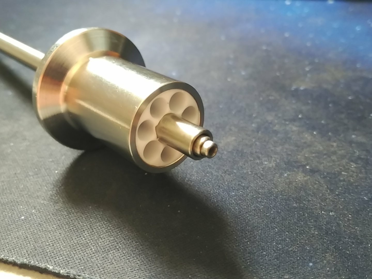
Endcap adapter from 45mm tube to KF40 for the fused quartz oven tube. Must be metal (can be 3D printed in aluminium, for example). Requires 12xM3*10mm screws AND 50OD*3,1mm O-ring.

Standard Tesselated Geometry - 2.97 MB - 10/19/2018 at 06:37

Download

View all 32 files

View all 45 components

  • Patreon!

    Nixie11/20/2019 at 08:36 0 comments

    So, a friend of mine held me at a figuratively gunpoint and made me put up a patreon to help quicken, to some extent, the project.

    https://www.patreon.com/user?u=14363159

    I myself got quite deep in my last job, so everything got put up aside-ish, but no more, as they had to fire me due to external factors to the company.

    So, meanwhile I get a new job, I will be able to put all the files in a more comprehensible format/shape, and look for better ways to make all the info avaliable.

    Also, i will post again about news and such, as I think I found a cheap-ish way to do a wirebonder, and sources for hotplates that make it not worth to build one yourself.

    More info soon!

    Btw, if you happen to share the patreon link on twitter or something, thanks in advance and let me know!

  • Silicon Overlords

    Nixie07/02/2019 at 08:02 0 comments

    So, meanwhile there is significant advancement, I made a discord channel for those interested in the subject.

    https://t.co/yLzVvEe0Kw

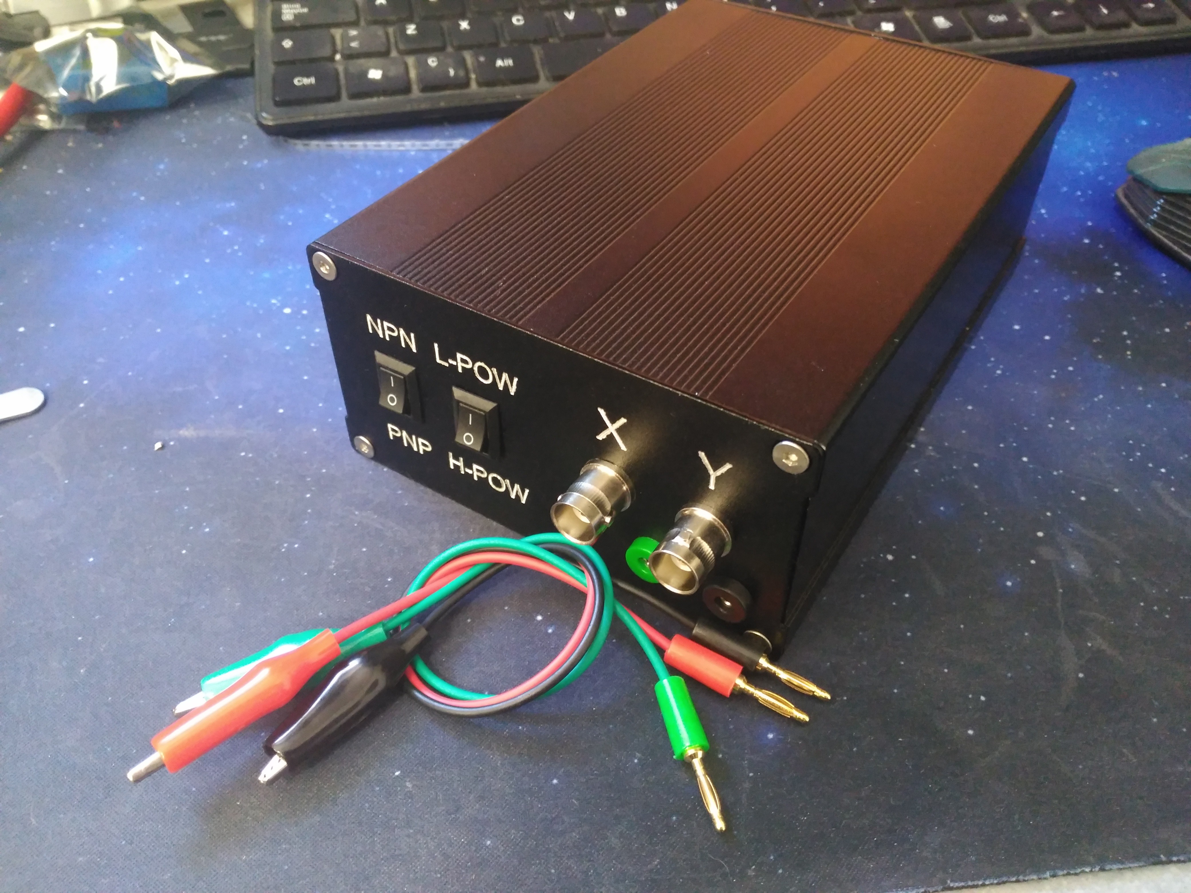
    On my side, finally foubd a job wich i enjoy AND pays well. XD

    I also have been finishing the curve tracer, located a possible source for low concentration HF, and bought a few more vidicon tubes for the e-beam gun, so I have spares to break without worrying much.

    See ya!

  • I ATEN`T DED!

    Nixie02/01/2019 at 10:12 5 comments

    Just in case anyone was afraid I had left this as is, I have not. I am busy right now finding a job in southern spain (wich is not easy, btw).

    Things are moving along slowly but steadily. Pieces are arriving from around the world, and knowledge is being amassed too.

    PCB's are being designed, built and tested.

    So, hold on, I'll be back soon!http://2.bp.blogspot.com/--cviN-3TQNY/UPftQbC8oLI/AAAAAAAAHlc/RLqHMC43ayQ/s1600/Fallout+Standby.jpg

  • Diode! ...Diode?

    Nixie10/18/2018 at 06:28 0 comments

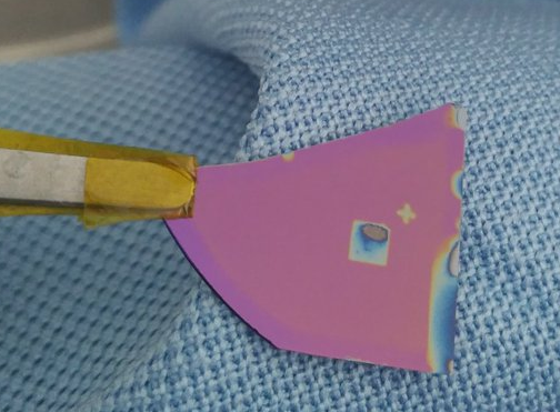
    First noticeable diode effect in N-type (phosphor) wafer, using Boron.

    Right now I'm stuck with N-type (Sulphur) doped wafers, so I'm using boric acid as boron source. When cooking it, it produces borosilicate glass on top of the wafer, wich, if you use too much of the dopant, makes for such a thick film that can't be really etched away. Luckily, a small window opened in the center of the test, and I could access the boron doped part. ^^
    https://pbs.twimg.com/media/DpuTko0XUAAqG1Y.jpg(after diffusion, before etching)

    Also, laser paterning is coming along nicely!
    2mm test square and "+" fiducial. Should have left in HF longer, but curiosity got the best of me. ^^
  • Doc Ock (final)

    Nixie09/09/2018 at 00:20 0 comments

    When we left, this was the general idea I wanted to achieve:

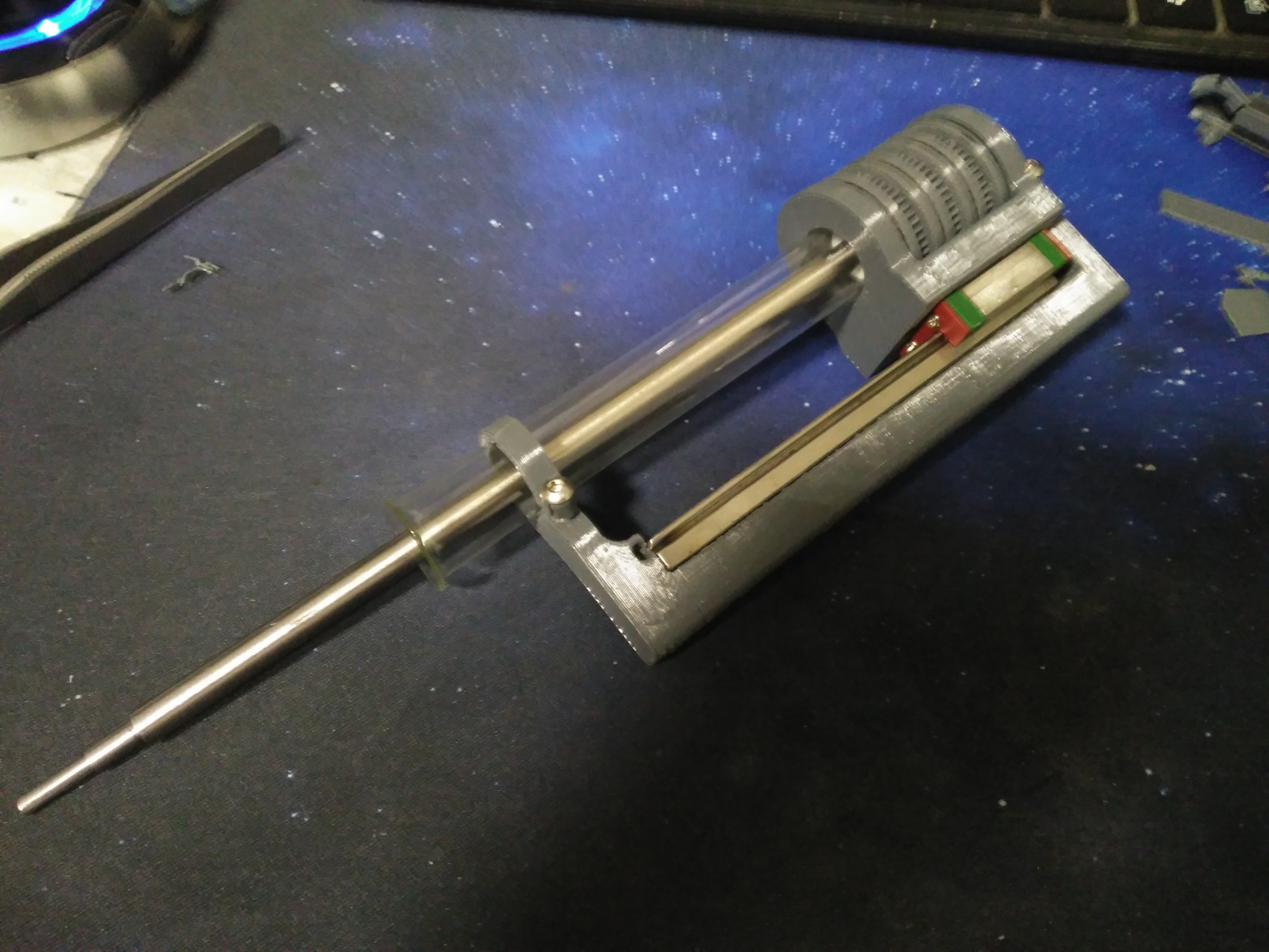
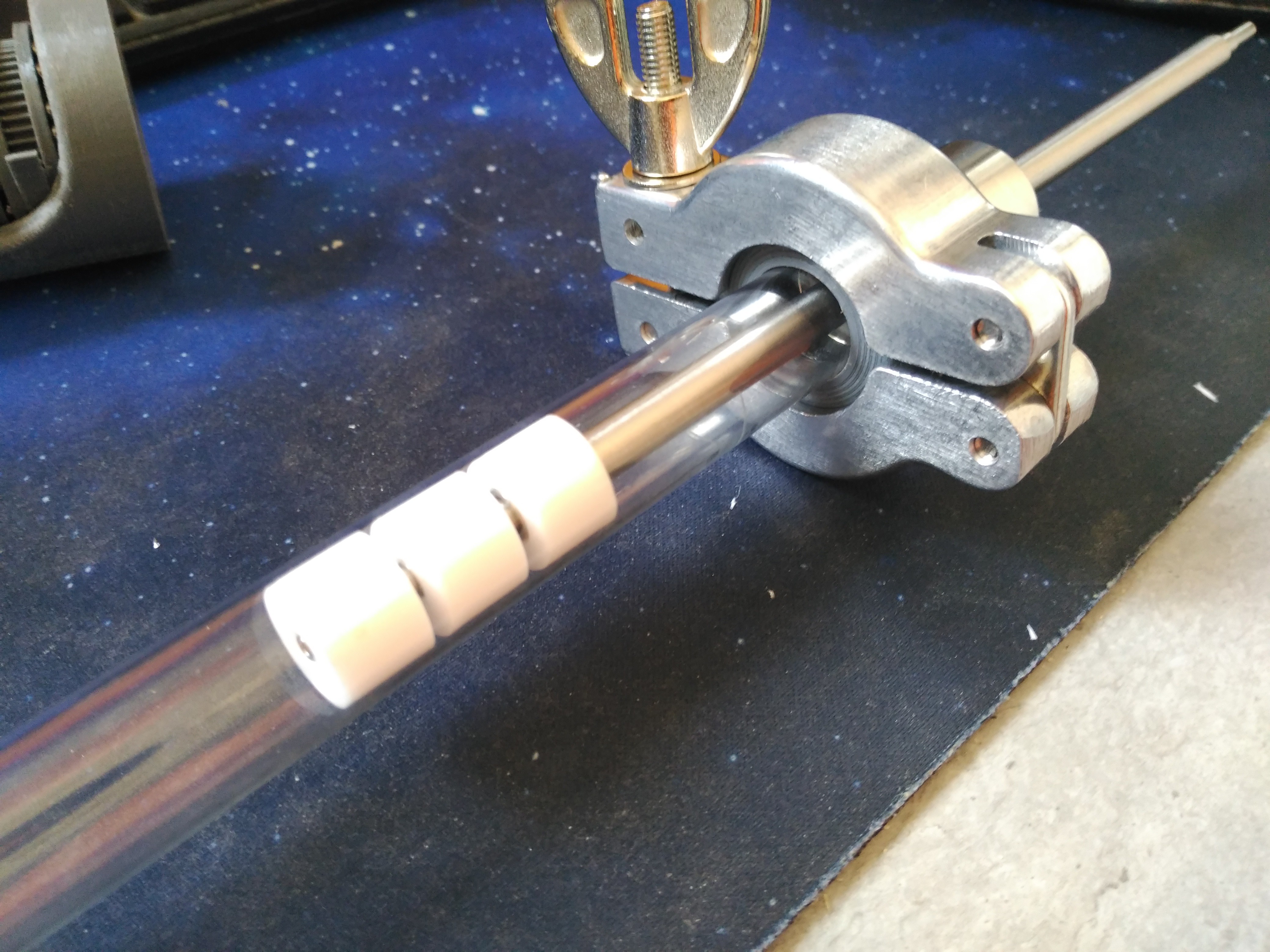
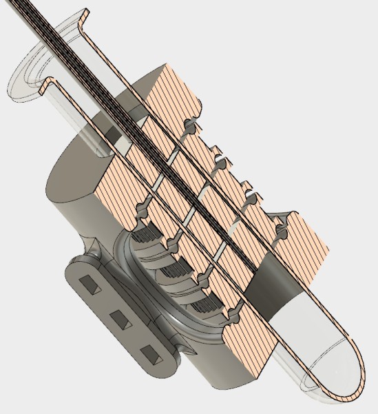
    A magnetic HVAC interface using a (modified) glass test tube for vacuum holding.


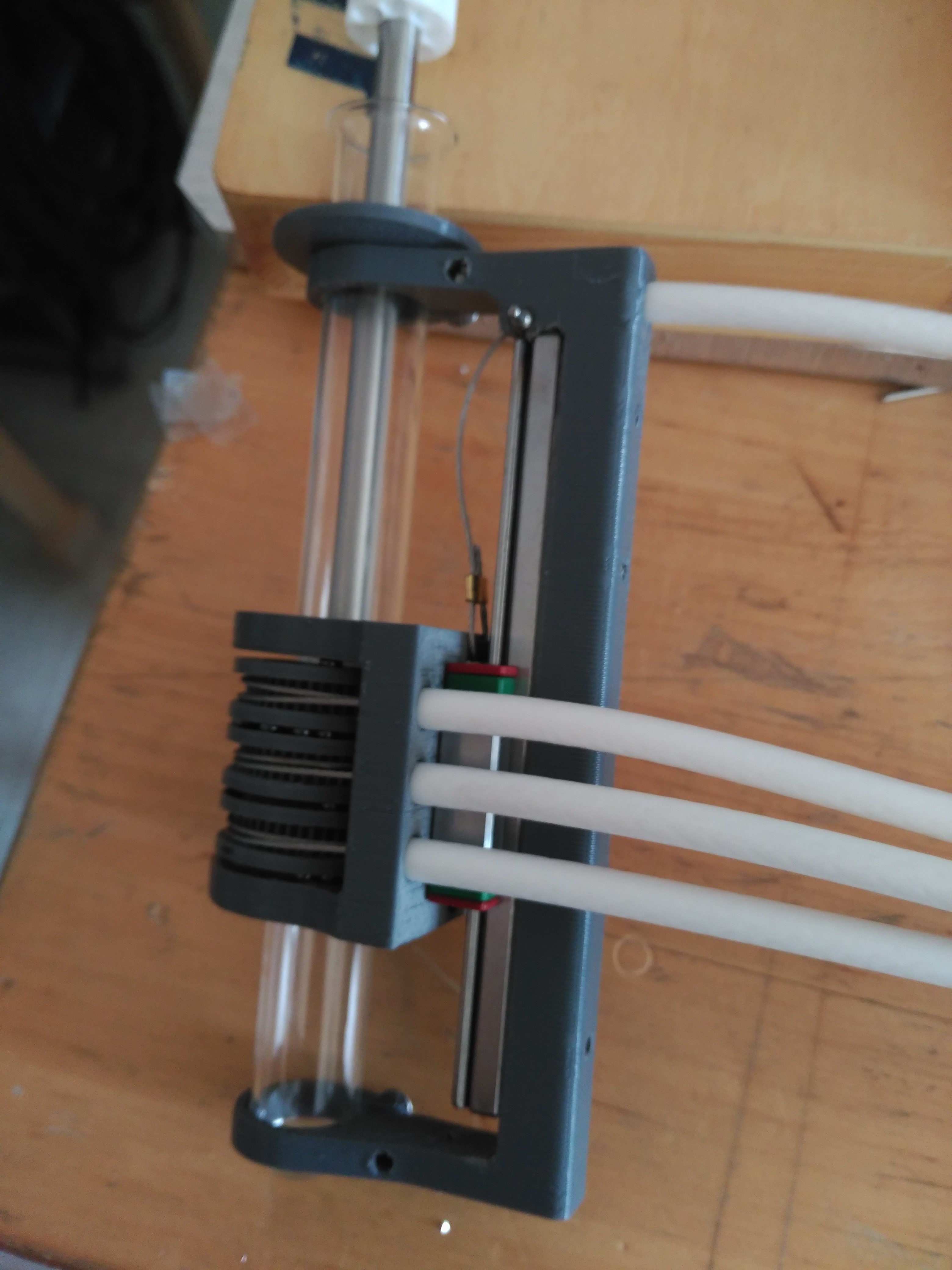
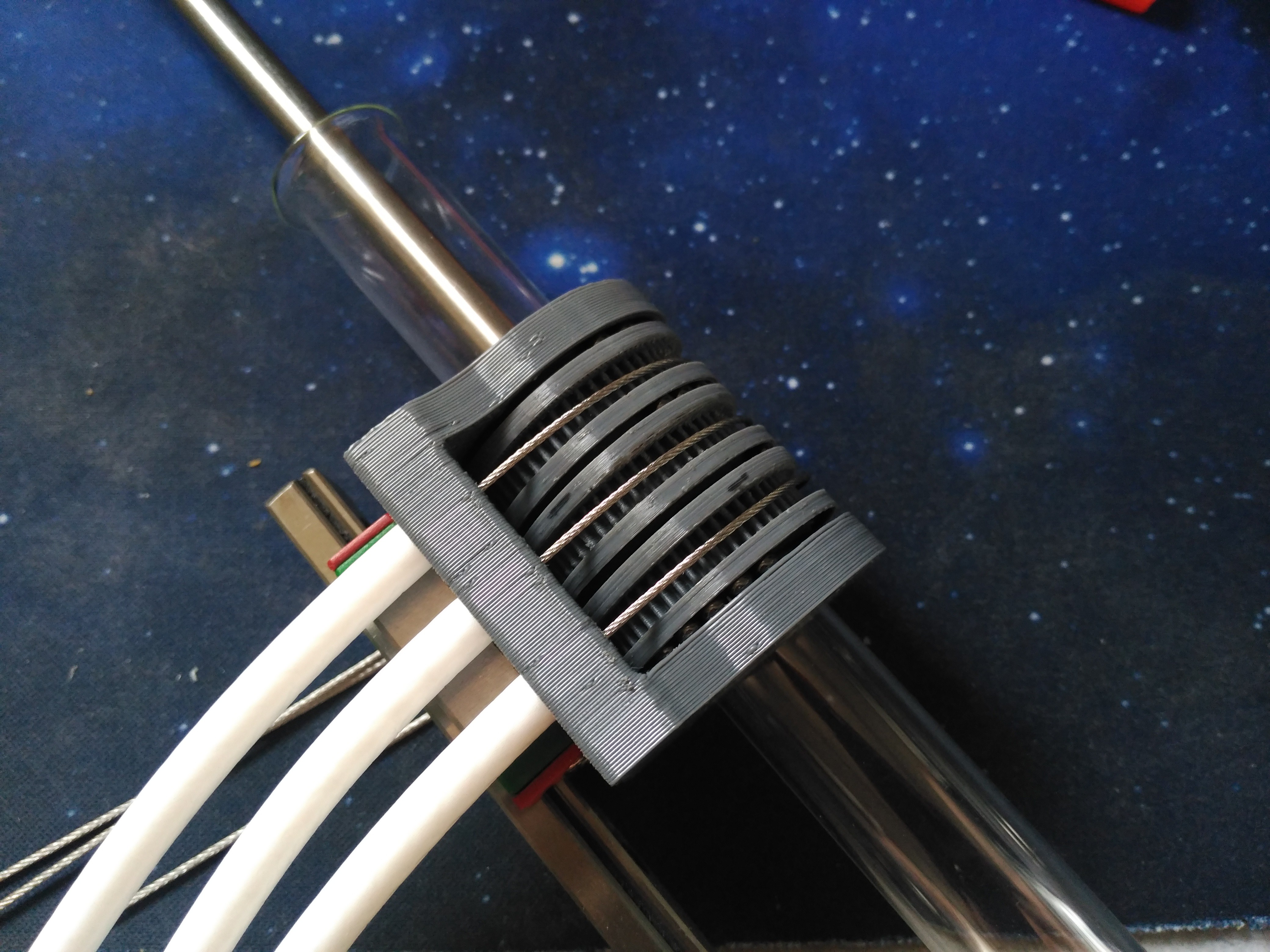
    First thing I adressed was the driver holder/actuator. Gear/rack mechanical coupling proved impractical, so I switched to bowden drive:

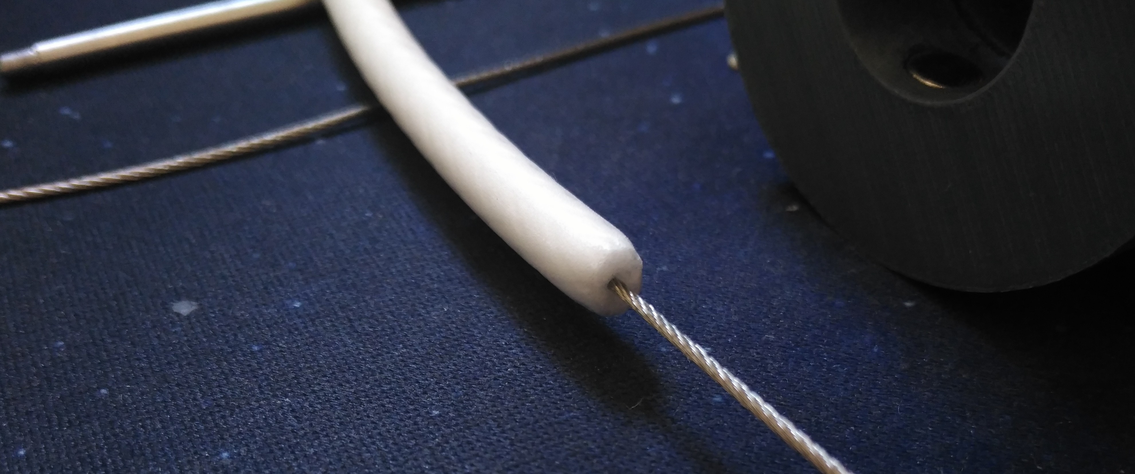
    I had thin braided steel cable in my workshop, for pneumatically pulling things in other projects. What I did not have was bowden tube of any kind!

    Coaxial cable, help me!

    UHF cable core is usually made either of poliethilene foam or, in higher grades, from PTFE. I wasn't as  lucky as the second choice, but for short distances and small forces, PU foam would work fine. (for future projects I did order PTFE tubes)

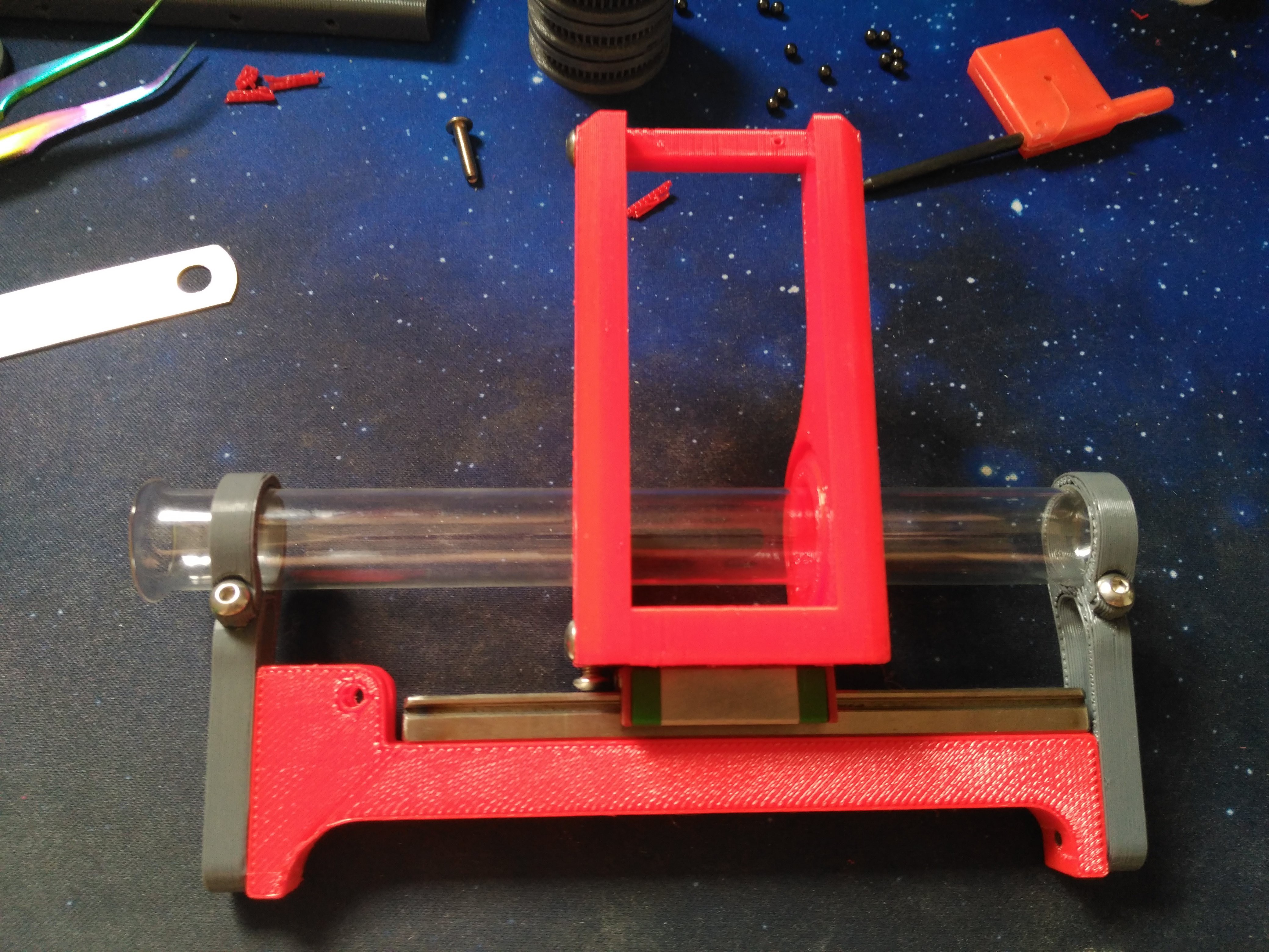
    A linear rail was added to the back to attach the motion driver to the test tube and provide Z axis movement/control.

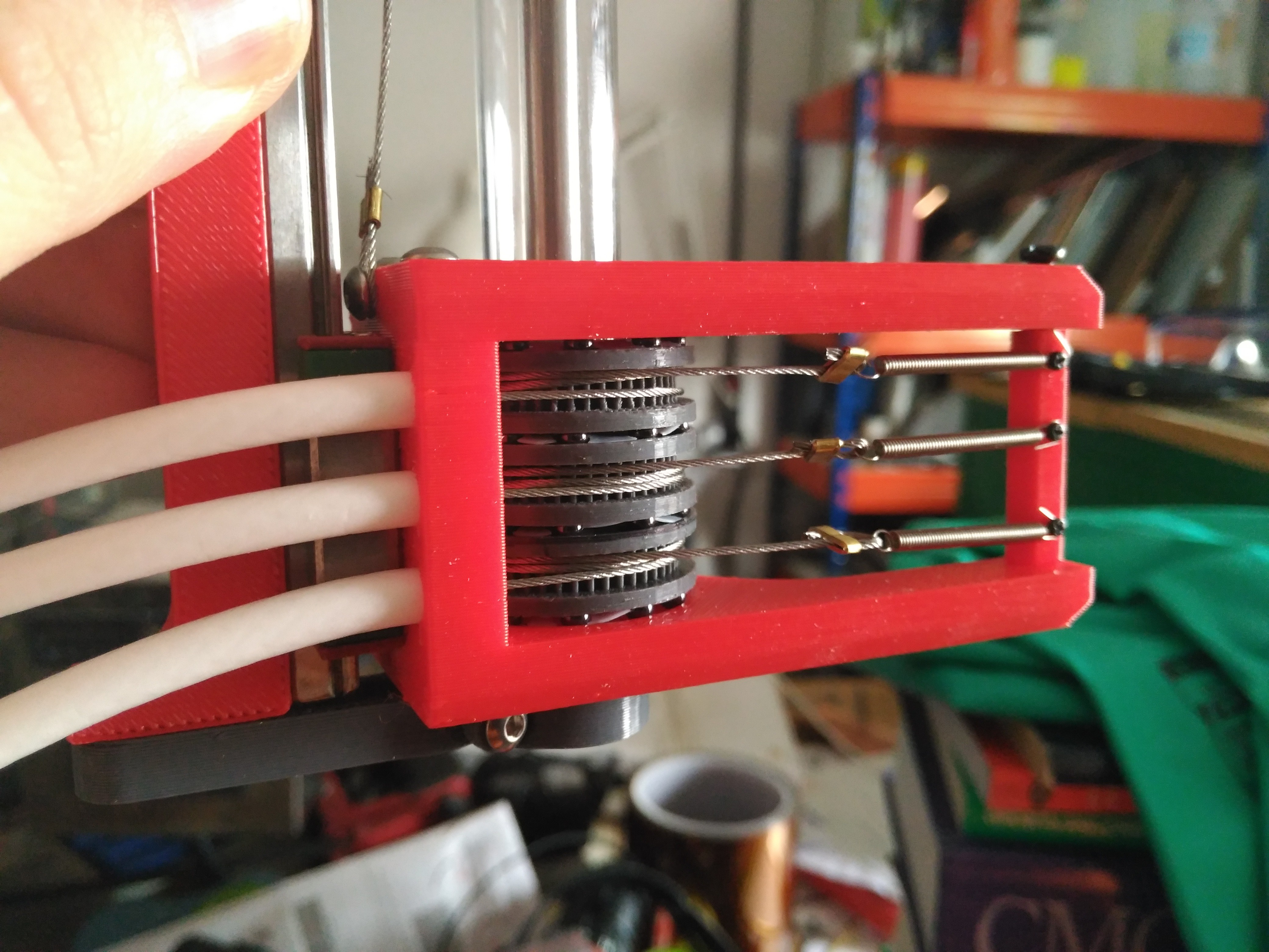
    Wich would also be bowden controlled:

    Springs on the other side of the bowdens would provide cable tension. However, altough the bearings could take it, they exerted much lateral force in the pulleys, binding the rotary motion, so, a second version with zero radial net force was implemented.

    The axis of the push/pull force in the cable sit in the same plane, nullifying the force exerted on the pulley (technically, it generates a twisting motion as the cable does not alignt with itself, but the bearings can cope with that easily)

    Also, the fixed test tube holder didn't really work, as each test tube is slightly different, so, the linear guide holder was made as separate pieces, making the tube supports adjustable.

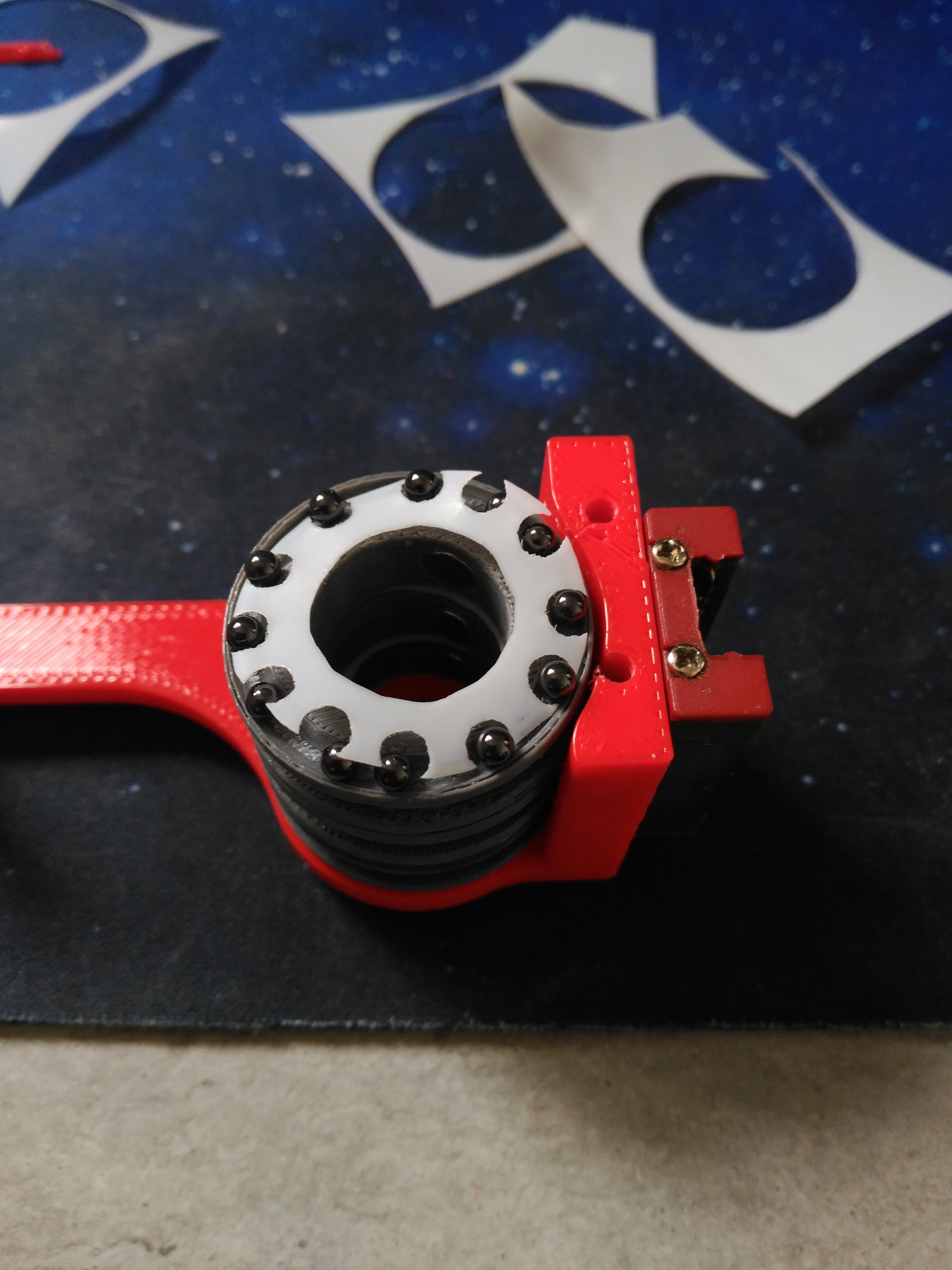
    Teflon ball cages where scissor cut so the balls would sit properly in the pulleys:

    Small sections of brass tube would be flat clamped to the cable to make connections.

    In action:

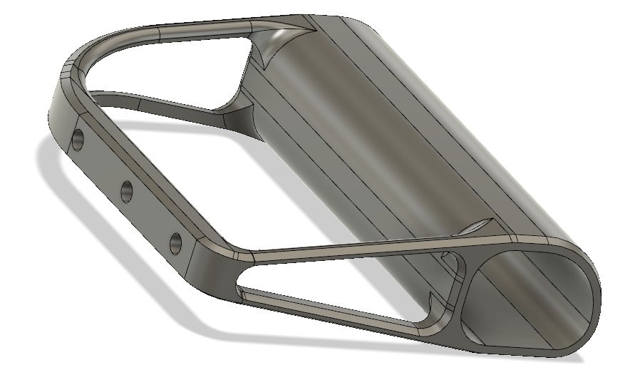
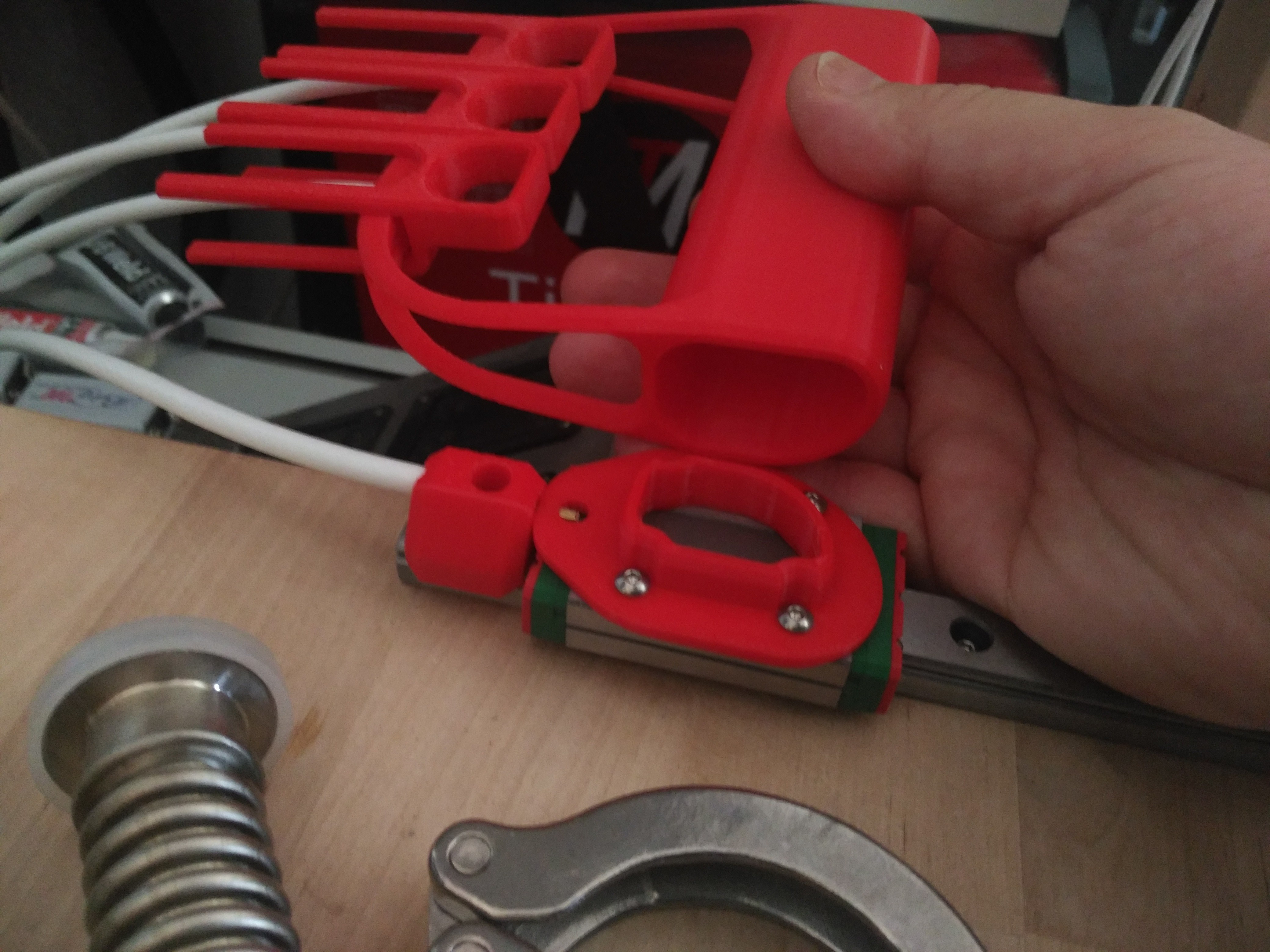
    After that, it was time to make a hand controller for it. So I mostly went nuts with the chamfer tool in fusion 360:

    That hand piece would get attached to a linear rail with an adaptor, wich in turn would be directly screwed to the sputtering table.

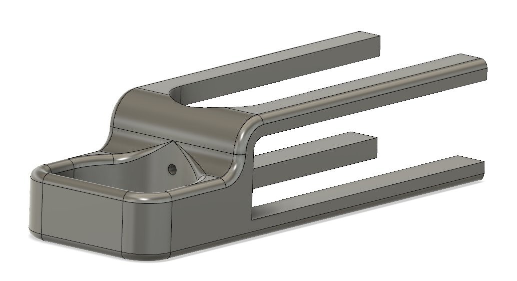
    The whole hand will move the Z axis, whereas each finger will have direct control of one of the pulleys with these finger cable pullers:

    And how does it work?

    AMAZING, if I can say so:

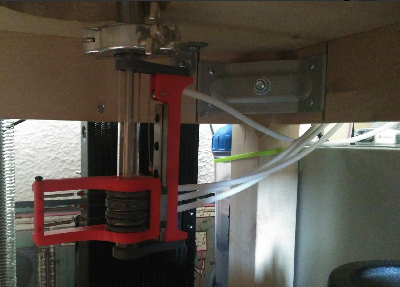
    Here's a bottom view of the assembly coupled to the vacuum chamber:

    All the bowdens where cut to the minimal lenght and lubed with silicone oil. For upper guidance/parallelism a PTFE guide for the metal parts was cnc cut:

    So what does all this accomplish?

    I now have a modular system with 3 coaxial axles with Z movement that I can employ for anything inside the vacuum chamber, WHILE it is operating.

    I can have different motion groups for different purposes and all I need to do is remove the internal magnet assembly, wich slides out into the chamber, and put a new one, with different end effectors/holders/targets.

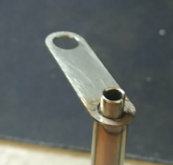
    Here, for example. I'm spot welding a small strip of stainless, in provision for the small arm that can move samples around:

    Instead of an arm, I can use it to put a plate over the samples and cover them until the sputtering is stable and clean.

    Or:

    I can have one arm with targets, and switch them at my convenience, while a second arm covers the samples meanwhile the changes (leftover sputter of a different material) stabilize.

    There are infinite possibilities for this, It is just a matter of what work I need doing inside the vacuum environment.

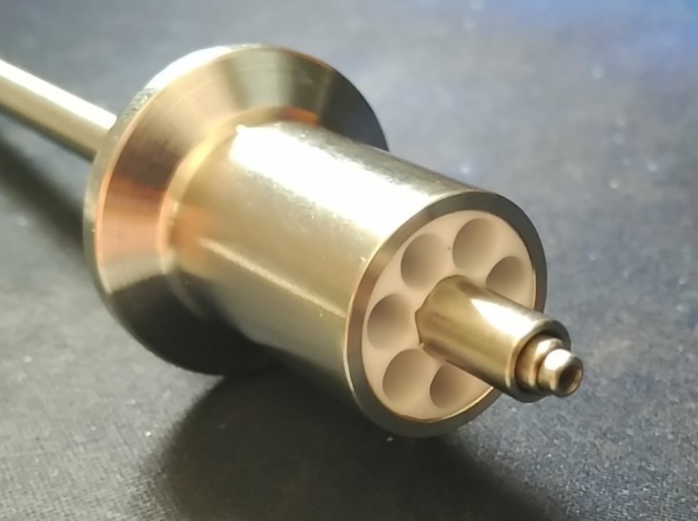
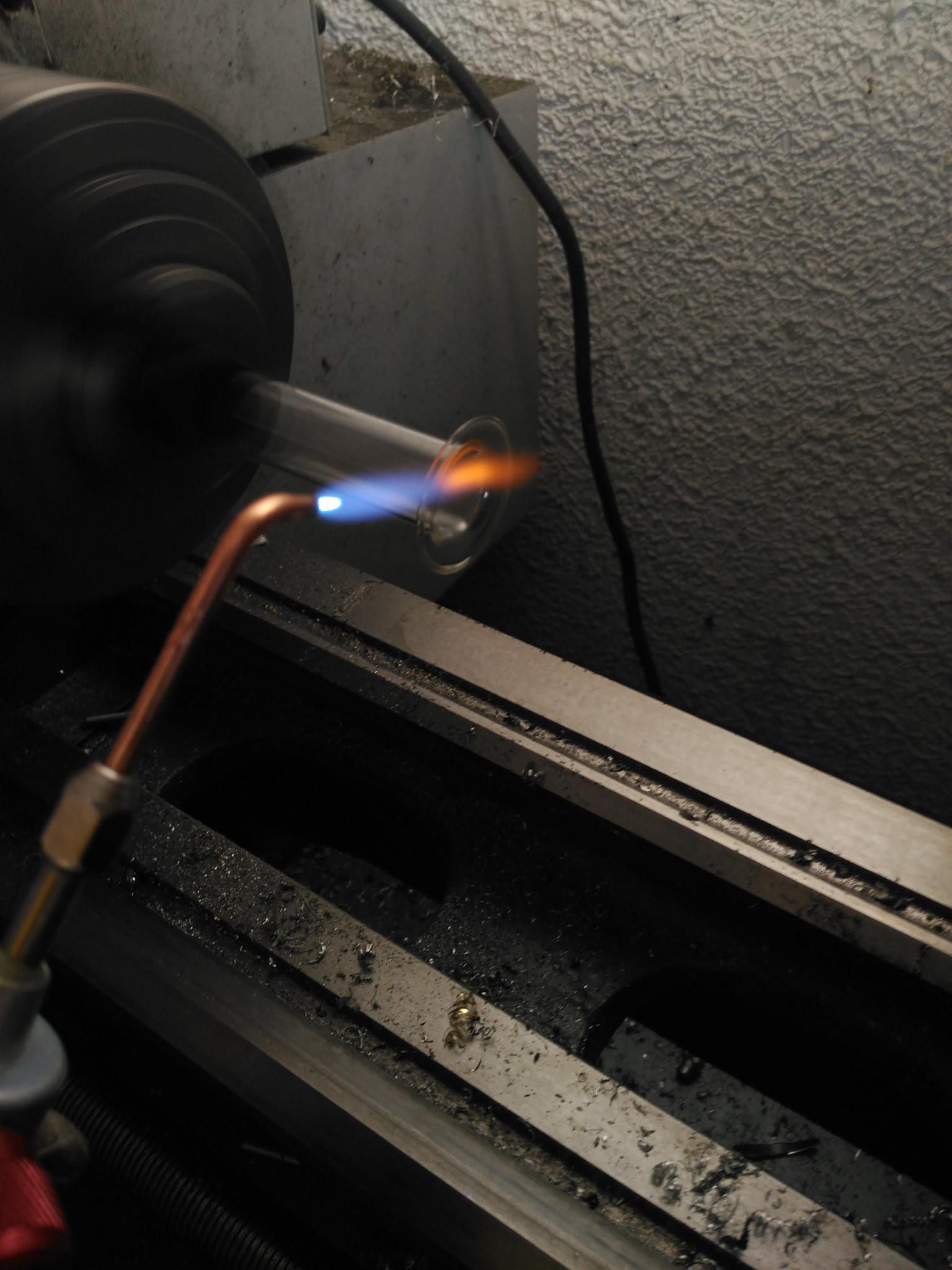
    Glass details:

    The glass test tube is hand-modified with an Oxy-torch in the lathe, so you can do everything at home, no need to depend on anyone for weird pieces.

  • Magnetic Trollscience.

    Nixie08/30/2018 at 17:01 0 comments

    Finally got around to fabricate the axle pieces for the magnetic coupling.

    Full independent rotation and coupled up/down movement.

    All sliding surfaces are made out of teflon.

    Machining the different magnet carriers:

    Those are press fit into the axles and magnets added.

    The external actuator needs to be redesigned now that everything works fine, that's for another update. XD

    See ya!

  • Hocus Focus.

    Nixie08/22/2018 at 14:19 0 comments

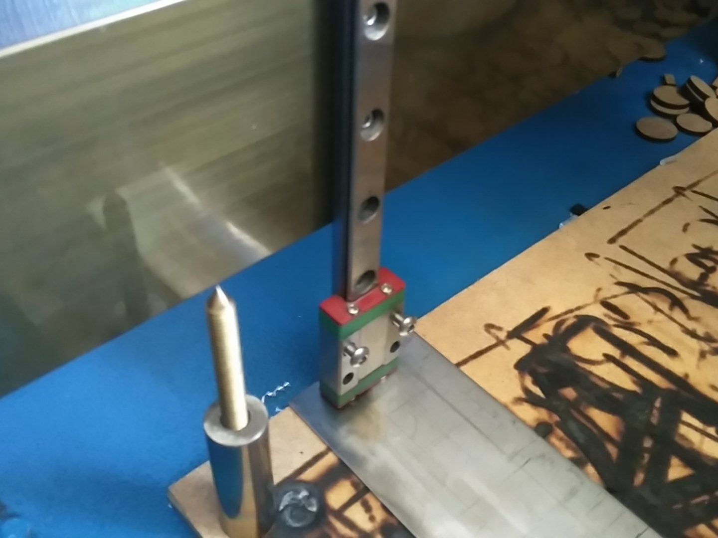
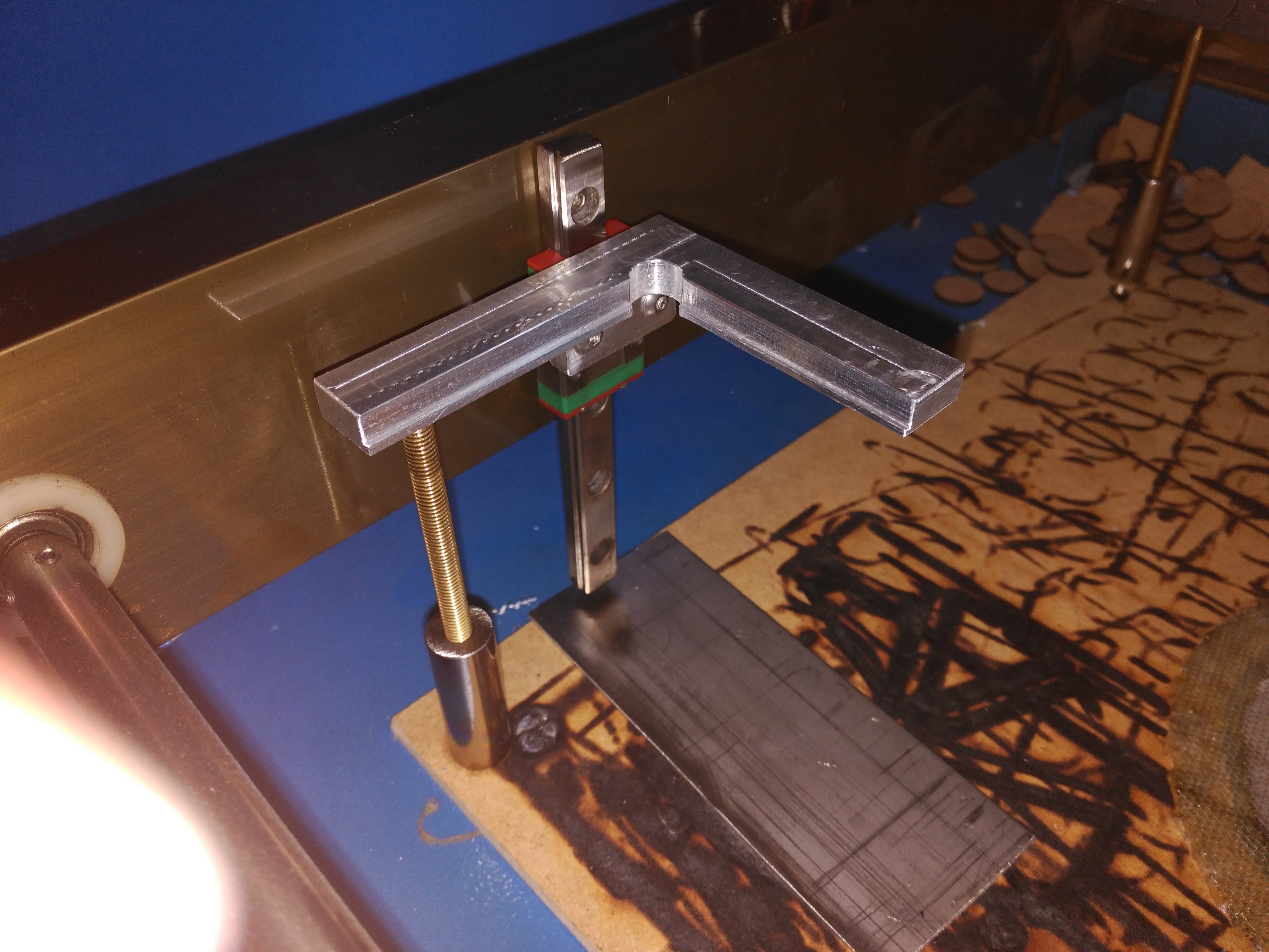
    Until now, I had been doing the laser litography tests with the machine as is. Nailing the focal point was tricky, if I ever found it.

    Once I started having better results with the technique (right in the above image) it was clear I needed a better way to find and mantain focus with the silicon.

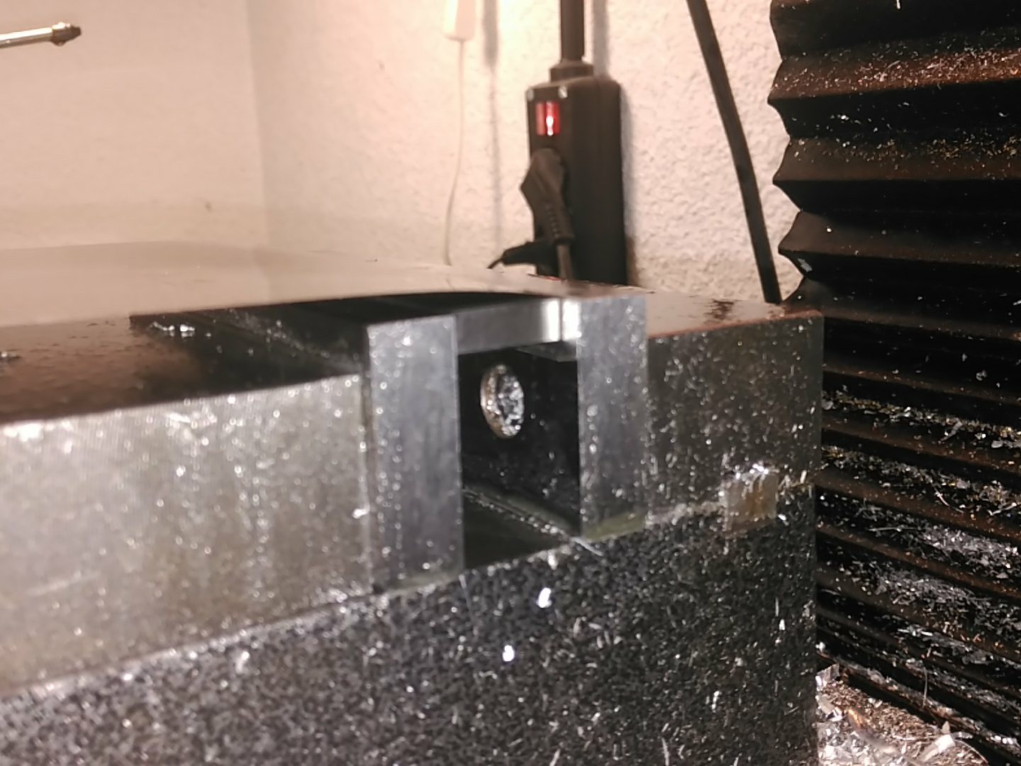
    The holder also has to be hollow, since the laser mostly goes through the Silicon, and having a surface just below the wafer, could prove problematic.

    So, holes where drilled...

    And a vertical linear rail was added:

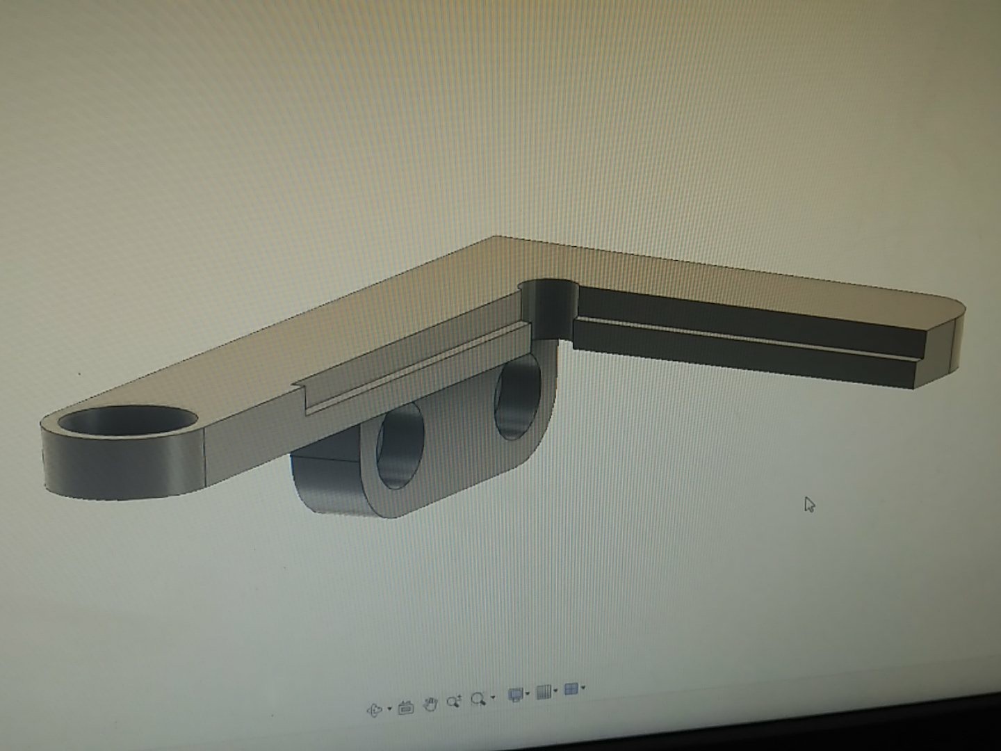
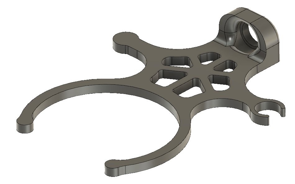
    The design requirements dictated the shape, edges and lengths, so there wasn't much to the design:

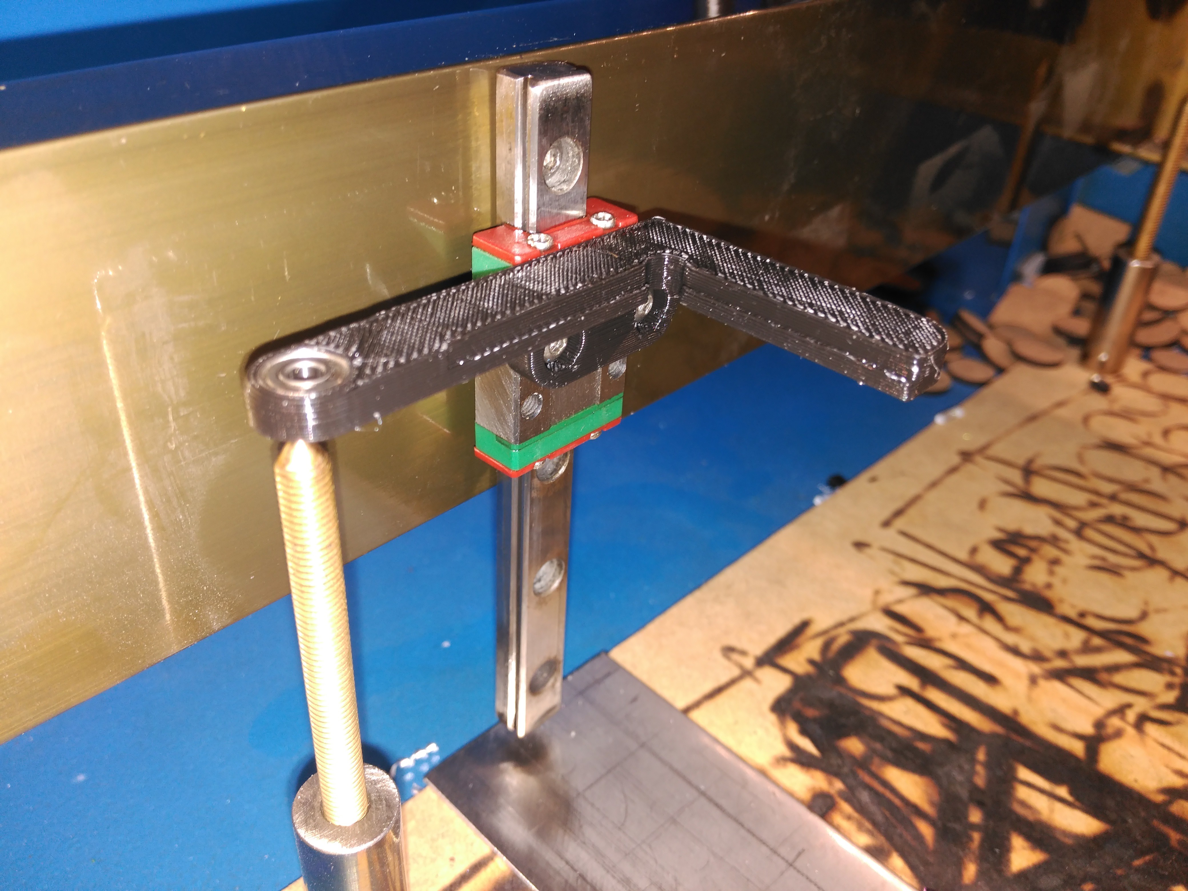
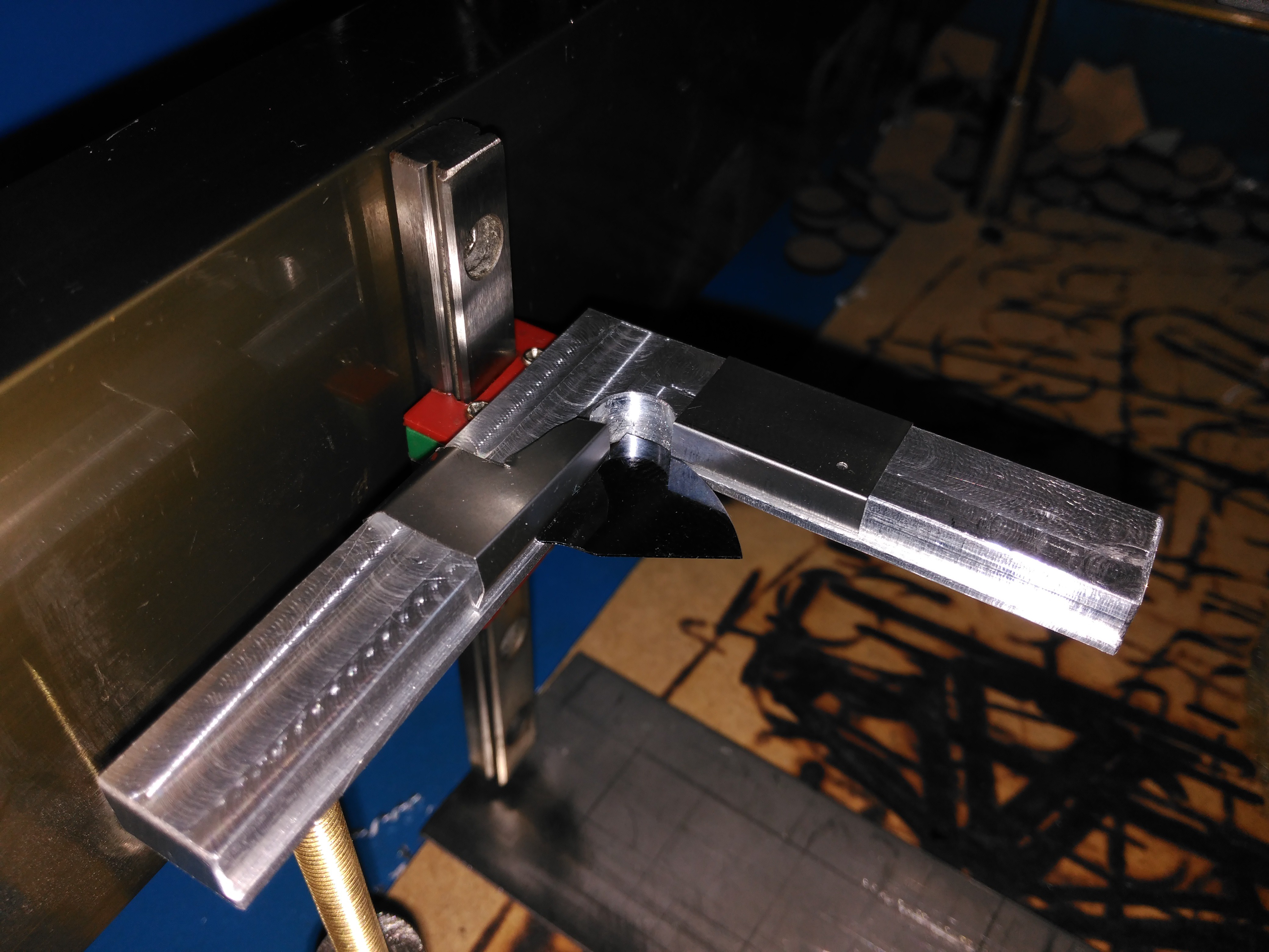
    This piece, working near a laser, should not be made out of plastic, however, for quick tests, I 3D printed it to have a feel of how it sat in the machine.
    (Just ignore the bearing, it was meant for something else, but it was not needed in the end.)

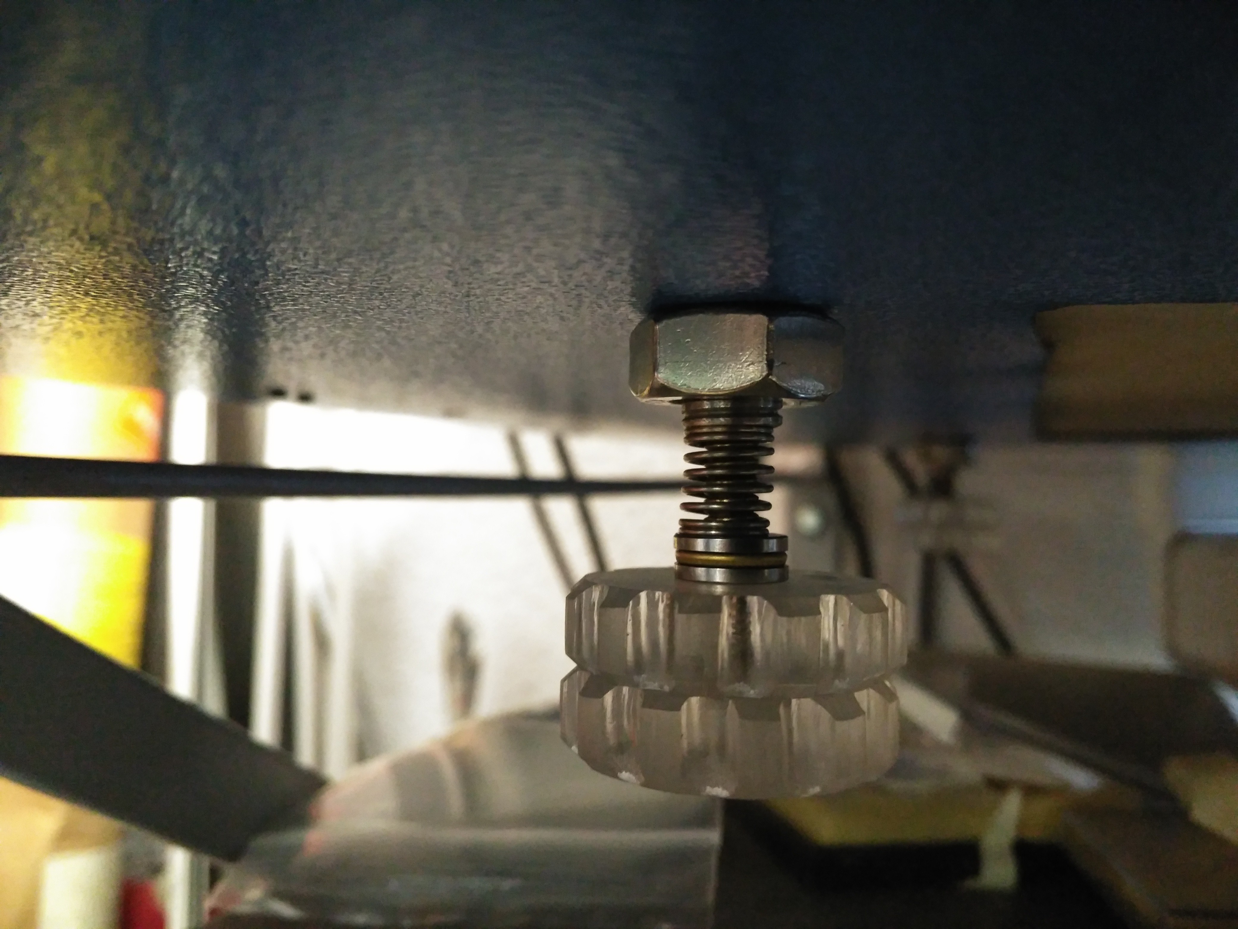
    I will be using the cutting height adjusters, however, just as they where, it could probe flimsy for precision height adjustment, so the screw was preloaded with a spring and an axial bearing to prevent twist resistance:


    Everything looked great, so I embarked in the machning. Nothing in it was size critical, only the mounting holes, so I preferred to hand machine it, as my mill can remove much more material than my cheap CNC router can.

    Holding is done through flat springs, sitting against the small 1mm ledges in the piece, and made pretty much like the cover in the hot plate:

    (The ones in the image are just temporary, better ones will be made. To prevent chipping, the side in contact with the silicon is rolled, so it presents a smooth surface.)

    Done!

    Now, let's keep R+D going!

  • Surprise Hot Plate.

    Nixie08/13/2018 at 17:38 0 comments

    Up until now, I had been using the oven at a lower temperature, as a makeshift hot plate/convection oven to dry thin fims.

    However, as I begin to use the oven for it's intended purpose (growin SiO2 and difussion) it becomes very counterproductive to use it for other things. So, a hot plate to dry the thin films was devised.

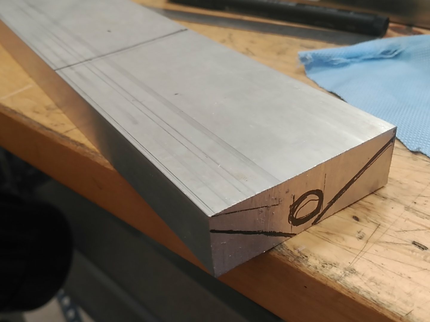
    A suitable chunk of aluminium was procured from the workshop, wich offered enough space for multiple pieces and could hold in itself the heating cartridge I had around.

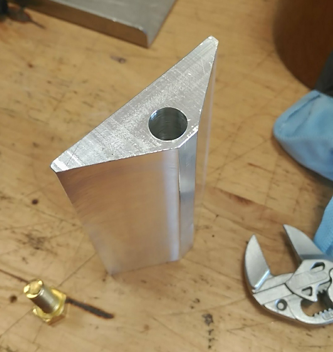
    Drilled and milled:

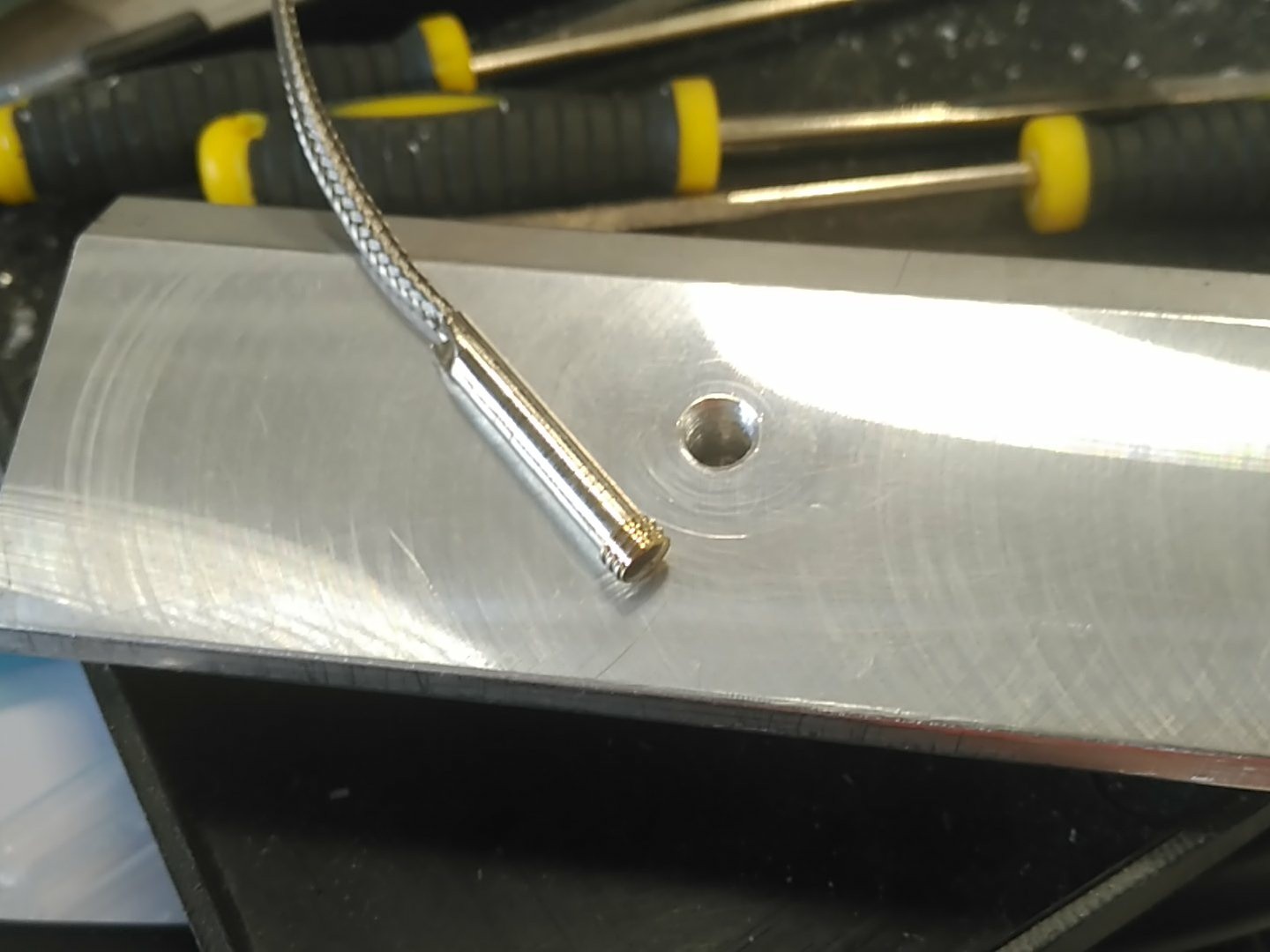
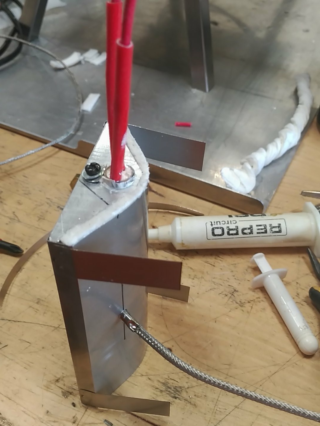
    For the K probe, the retention screw had a weird thread I didn't had a matching tap for, so I ended threading the probe itself to M5 and screwing that into the aluminium block. Having it's head sitting just 3mm below the surface of the plate. Plenty of thermal compound was employed.

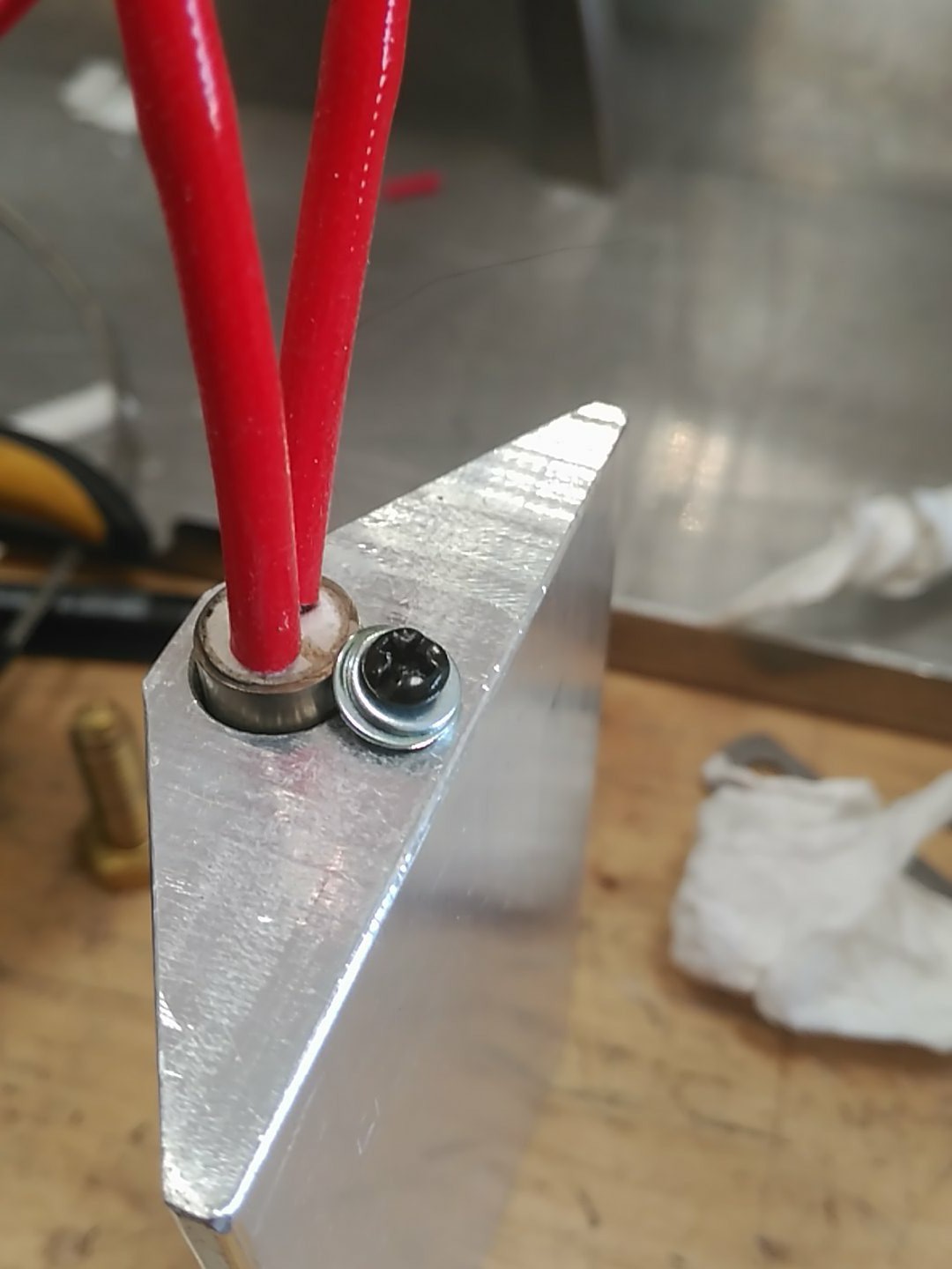
    The heating cartridge was retained with a screw and plenty of thermal compound too.

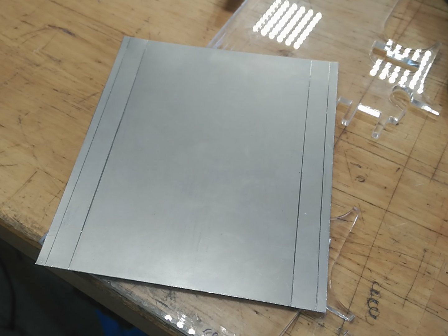
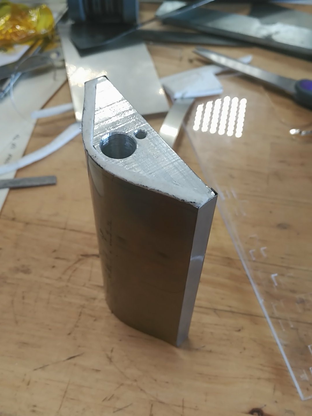
    Finally, I wanted to add some termic isolation to the bottom, so the assembly could be made compact. Ceramic matt tends to be fragile, so mechanical subjection is not recomendable. Instead, I scissor cut a piece of solder paste stencil and marked it with a cutter.

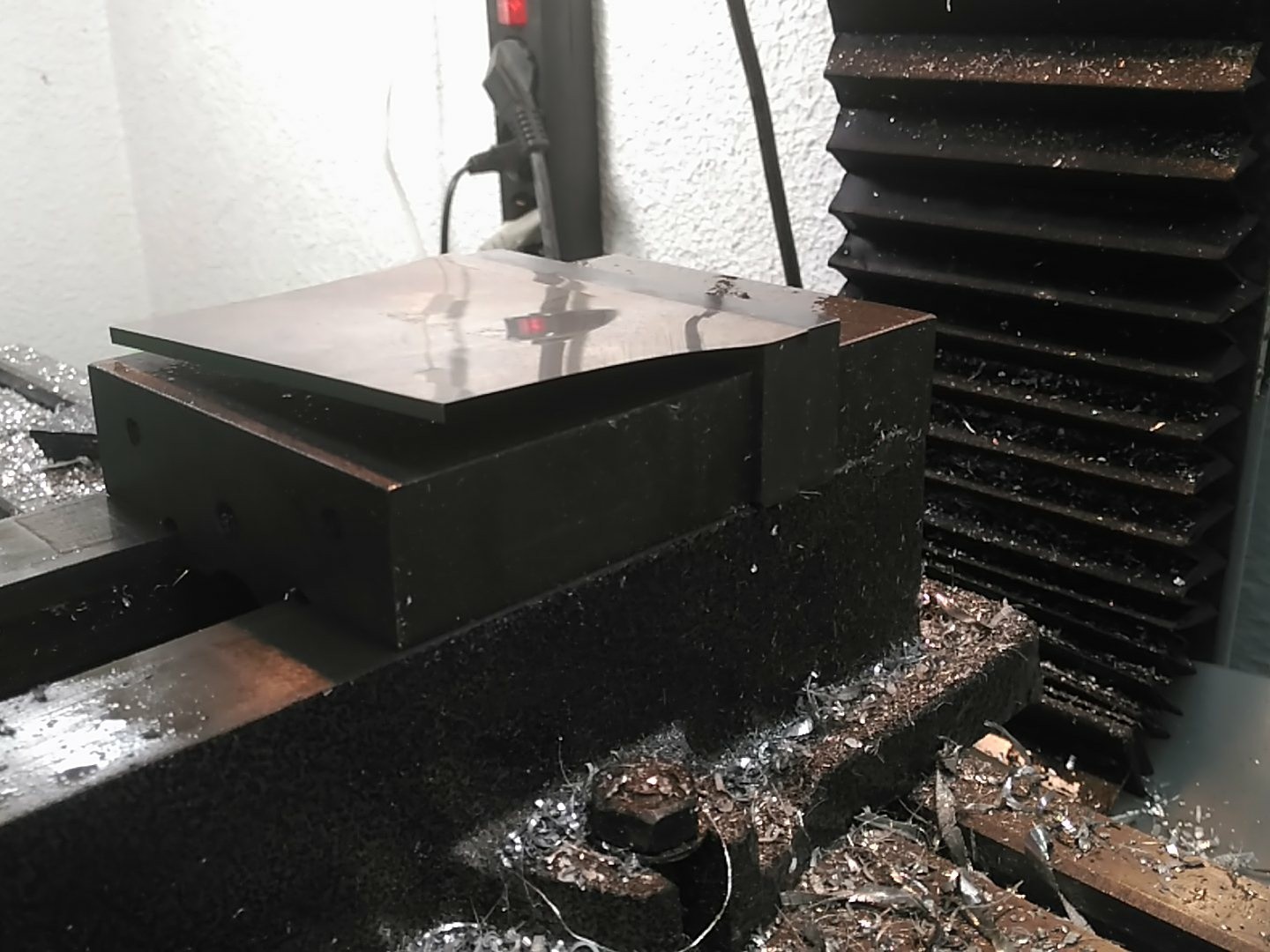
    Clamping it into a vice, it was first hand bent and then shaped with a nylon mallet:

    The inside corners where bent using a spacer:

    With that and careful measurement, a super nice bracket for the ceramic matt was done:

    To further isolate the electronics from the plate, sheet metal legs where spot welded to the plate:

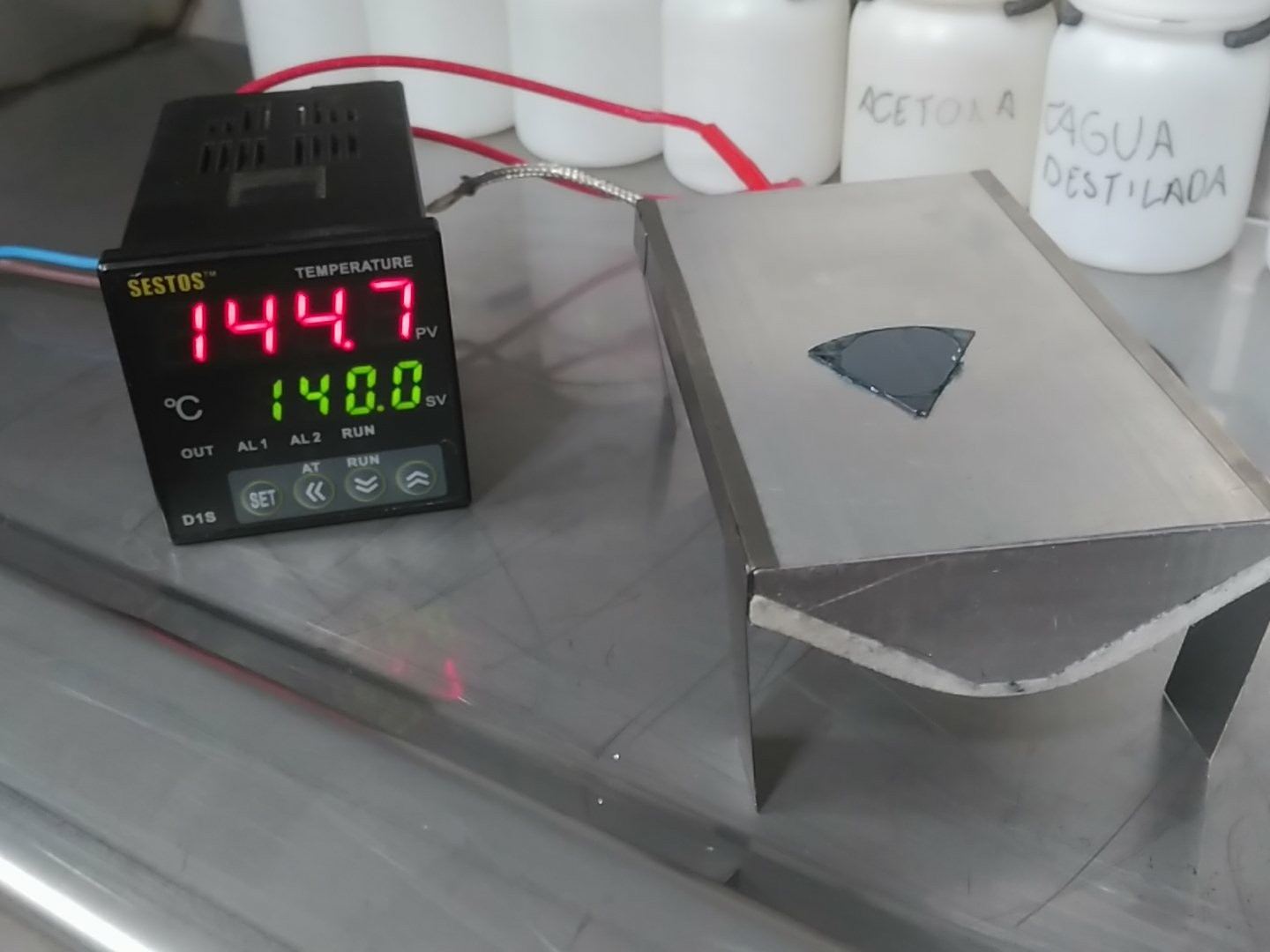
    With that, but pending a different temperature controller with SSR capabilities, I connected it to an old controller I had around, and for now, I have a sketchy, but working hot plate!

    Once I get the definitive controller, everything will be made much compact, with the plate on top of the controller + SSR, a nice case and some form of heat shield so you can't accidentally touch the hotplate sides.

  • Ready, steady...GO!

    Nixie08/08/2018 at 13:38 0 comments

    Finally, all pieces are in place.

    The gear has been built. The oven, the sputtering rig, the spin coater and the fume hood.

    The chemicals have been bought.

    All thar remains is to test, test, test...and then more testing. I would hope to have some kind of semiconductor device (a diode?) by september first, time will tell, some say.

    For now, I would recommend to look at my twitter account where I post my findings and experiments in real time (using it as a kind of log/documenting process).

    https://twitter.com/nixie_guy

    Points of update in Hackaday.io will be more or less the following:

    1.- Succesful PMMA milling on a silicon substrate.

    2.- Succesful SiO2 etching with HF 2%

    3.- Succesful alignment of features for multiple masking process.

    4.- First dopings.

    5.- First DIODE.

    6.- First aluminium sputtered connection for a diode.

    7.- Realiability of repetition.

    After that, FET tests will begin, wich are another can of worms.

  • In the eye of the Bottleholder.

    Nixie08/06/2018 at 09:45 0 comments

    With mostly everything ready to begin tests, bits of safety remained to be solved.

    Since I will be working with dangerous chemicals, I didn't want to have the small bottles of them hanging around all over the place.

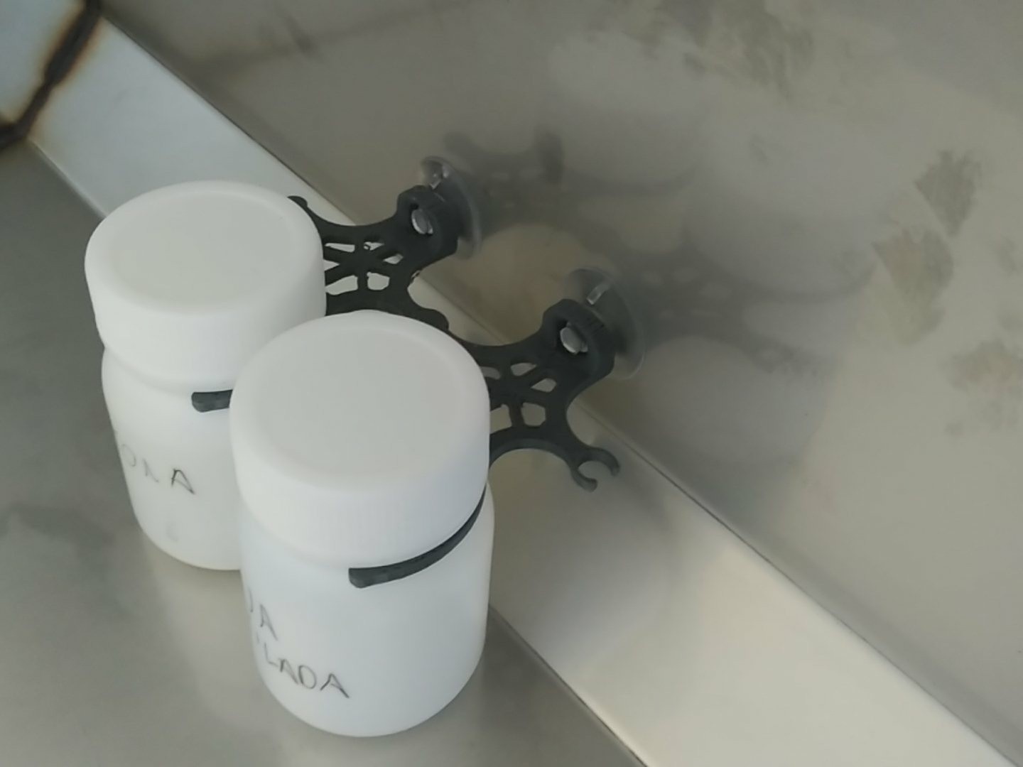
    Thus, I came up with this:

    This holds onto the bottle neck in the front and has a suction cup in the back, so it can be attached to the wall of the fume hood. It is also interconnectable with other pieces, so it can form a neatly arranged array:

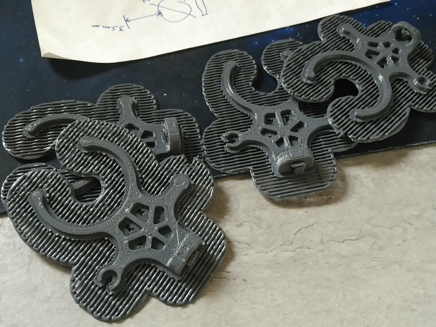
    They are easily and fast 3D printed with a 0,6mm nozzle:

    They should be improved by changing the 2D side connector (isc clamp) to a 3D version (ball clamp) so they can't slide out, altough that would be difficult with bottles in each holder.

    Huge array, in preparation of semiconductor tests:

    And a small video of it's use:

    See ya!

View all 39 project logs

  • 1
    Semiconductors @ Home - Compendium

    Please, check "Semiconductors @ Home - Compendium.pdf" in the files section, it has all the knowledge gained during the developement of this project machinery.

  • 2
    Semiconductors @ Home - Cookbook!

    Please, check "Semiconductors @ Home - Cookbook!.pdf" in the files section, it has all the practical instructions developed with the previously built tools.

    This file will be updated constantly, as I go along figuring out the processes themselves, so check occasionally for updates.

View all instructions

Enjoy this project?

Share

Discussions

excitedbox wrote 04/05/2021 at 03:59 point

I just found this design for a DIY diffusion pump made from a cocktail shaker. https://diyvacuumtubes.com/steampunk-diffusion-pump-t14.html They have a few other designs on the forum as well. Only hand tools needed for this one.

  Are you sure? yes | no

Alejandro FIgueroa wrote 06/21/2020 at 06:18 point

Hi Nixie , thank you for sharing with us this project , what you are making here is amazing!

  Are you sure? yes | no

Nixie wrote 07/14/2018 at 09:21 point

@Julian Maybe, I'm in the early stages, so I can't say. But in the future I'm open to all lines of fun stuff I can get my hands on. ^^
  Are you sure? yes | no

Julian wrote 07/14/2018 at 08:22 point

So when you get this all working, what kind of feature size/layer thickness do you think you're likely to be able to achieve?  Do you have any way planned for measuring the results with high accuracy?  Also, you say you're only planning on using the sputtering for producing interconnects and gate layers, but could you also use the same technique to lay down multiple semiconductor layers?  Perhaps producing bipolar SiGe transistors or similar?

  Are you sure? yes | no

Nixie wrote 07/14/2018 at 08:36 point

Probably way too big to be useful for a while, but that is mainly due to the photolitographyc process source. The CRT tube has a too short focusing lens to do really small dot size.
As for layer thickness, that is a different thing. Sputtering can yeld as thin a layer as you want, and difusion thickness is a matter of time/dopant density.
As for metrology, I'm not worrying about it yet, since, as said, the first attempts won't be small enough as to need critical measuring.

The project objective is to demonstrate it can be done (building most of the tools at home), but it is a long term project, with much to learn and investigate (and share on how-to)


  Are you sure? yes | no

Julian wrote 07/14/2018 at 08:55 point

My interest is in whether this approach can be used to build an integrated circuit with resonant tunnelling diodes, which are p-n junctions with the addition of very thin (5-10nm) heavily doped layers close to the junction location.  Which, if you lay them out vertically, sounds like it ought to be achievable.

  Are you sure? yes | no

Nixie wrote 05/14/2018 at 13:07 point

@ivan003003  (I can't answer directly to your messages, Hackaday.io is weird sometimes).

Mmmm...what kind of oxide you would like to sputter?,

Altough in any case, the cost of assembling a machine like this is around 1000€, with that surely you can gold coat many pcb's.

  Are you sure? yes | no

ivan003003 wrote 05/14/2018 at 13:37 point

I don't know yet,but maybe the graphite powder or Si Wafer,they could be excellent,especially the Si Wafer on the copper.

https://www.ebay.com/itm/Si-Wafer-SET-D40-mm-Silicon-Monocrystalline-24-pcs-in-box-/323250767065

  Are you sure? yes | no

Nixie wrote 05/14/2018 at 13:48 point

I bought two days ago the same set!!!! XD!!!

  Are you sure? yes | no

ivan003003 wrote 05/14/2018 at 14:25 point

Впечатлительно ;)

  Are you sure? yes | no

ivan003003 wrote 05/12/2018 at 01:14 point

I have a question.

Sorry for my poor english,but if you don't understand something,then pls don't hesitate to ask me details.

So my question is :

By using this Sputtering machine (Pvd) can i go to plate the copper traces on my pcb's antennas to defeat the skin effect ?

I can't afford to plate my pcb's with the real gold or silver,so for this reason im asking you if this machine can done the same job instead of gold plating :)

Thanks you very much!

  Are you sure? yes | no

Nixie wrote 05/13/2018 at 07:19 point

I do not understand the skin effect part. What would you like to cover the antennas with?
Sputtering can do insulator materials, but it requires radiofrequency to do it. This is a DC sputterng machine, easier to build.

  Are you sure? yes | no

ivan003003 wrote 05/14/2018 at 02:57 point

Hi there.

The skin effect in my case it's an psychic phenomena.

Basically when you are going up to Ghz range,the RF signal is not anymore linear.

Instead to circulate only on the geometrical traces of the antenna,it's goig to be chaotic &  unpredictable.

So for this reason in RF tecnology,the parts that are working at high frequency are always plated with gold,silver etc.....

At this point my idea was that:

Go to attach at the textolite an soldering stencil and then put the pcb in the sputtering machine to plate the antenna with some dioxide generated inside the pvd machine.

In fact it's just an idea to experiment,i'm not sure if this kind of thecnology could solve the problem of the RF Skin effect... just saying :(

  Are you sure? yes | no

ivan003003 wrote 05/14/2018 at 03:21 point

Actually i'm planning to draw on a pcb an Double-quad 2.5Ghz wi-fi antenna.

I will order it on pcbway or pcbcart (not yet sure);

so when i will done my order,the gold plated traces for this kind of application it's obligatory.

The gold plating in my case is rising for a lot the cost of the final product,but in any case by doing this there's no sense to do it without gold plating for an antenna based on Ghz's range .

  Are you sure? yes | no

heye.everts.1 wrote 05/09/2018 at 08:01 point

How do you control/measure the pressure in your vacuum chamber? 

  Are you sure? yes | no

heye.everts.1 wrote 05/09/2018 at 08:38 point

nevermind just browed through the comments and found it :-)

  Are you sure? yes | no

Nixie wrote 05/09/2018 at 11:58 point

XD

Also, since the pump motor uses a VFD, I can also tamper with the pump rpm to control the pressure.

  Are you sure? yes | no

zakqwy wrote 05/02/2018 at 20:27 point

congrats on the win! seems like you already know this, but be _really careful_ around HF. make sure you have a tub of calcium gluconate gel around.

  Are you sure? yes | no

Nixie wrote 05/02/2018 at 23:44 point

Any reminder of how dangerous is HF is always welcome in my agenda.^^
Yes, that's the first thing I'll buy before purchasing the chemicals, and thankyou for the cheering ;)

  Are you sure? yes | no

Mr. Ike wrote 05/03/2018 at 08:47 point

Great work!

I would say the same thing as Zakqwy. I work in this industry (Building sub-modules for a certain litho systems supplier) and HF is one of those things that makes me say: No, thank you. Lucky for me I have only had to deal with it once. Apart from having  a supply of Calcium Gluconate on hand, find a instruction sheet for medical personal on HF exposure and have that on hand in printed form. That way, IF god forbid something were to happen you don't have to explain anything and can just point. Something like: https://www.honeywell-hfacid.com/?document=hf-medical-book&download=1

  Are you sure? yes | no

Nixie wrote 05/03/2018 at 09:51 point

Thankyou ^^, will follow that advice too.

Imagine my face when the suplier said it "only" served the HF in 72%...

I was WTF, I'm not going to buy that!!!!!

Luckily they will dilute it for me down to 10/5% (5% If I can choose).

  Are you sure? yes | no

RoGeorge wrote 04/18/2018 at 09:04 point

Oh, gotta see this!
:o)

  Are you sure? yes | no

Nixie wrote 04/13/2018 at 03:45 point

@Keegan Reilly (for some reason .io doesn't allow a direct reply to your comment  :/      )

As long as you have fun, it will amount to something, I'd say. ^^
I'm using a Fieldpiece SVG3 micron display. There are some in Ebay at somewhat decent prices. Be careful with any of those, they can have "weird" connectors. (this one has a 1/4SAE connector, for wich I machined an adaptor to M8 (with gasket) to be able to connect it easily to other equipment.
If you achieve a stage (see what I did there? XD) where you are going to test the turbo, it will only indicate rough performance, since should the turbo work, it will go way below 1 micron.
In my head, even a turbo that can go from my pump's 50 microns to 1 micron or below, is somewhat justifiable for certain experiments). Really good mechanical vacuum pumps can directly achieve 1/0,1 microns, but at a (monetary) cost, obviously.

Going back to gauges, as said, if the turbo works, you'll end needing something along the lines of a pirani gauge or similar, again, there are some on ebay. Can't recommend any, since I'm not in that kind of vacuums yet/near future.

  Are you sure? yes | no

Keegan Reilly wrote 04/15/2018 at 22:11 point

Sounds good, thanks!  Yeah, the .io is weird sometimes.   I'll let ya know if I get anywhere with it...

  Are you sure? yes | no

Keegan Reilly wrote 04/12/2018 at 01:59 point

Very cool!  I've been thinking of dabbling in the vacuum space too, you've inspired me to pick it up again. I want to make an accessible (cheap) turbomolecular pump (easier said than done of course).  What gauge are you using to measure your vacuum?  

Also have you seen anyone use Pyrex mixing bowls as a chamber?  

Awesome work, and documentation, thanks for sharing and good luck!

  Are you sure? yes | no

Nixie wrote 04/12/2018 at 09:02 point

Glad it got you engaged, and yes, I know your tesla pump turbomolecular project too!

Did you know that nowadays, turbomolecular pumps are a hybrid of a turbine and a tesla? They call it "drag stage" and it sits behind the bladed section, having just like a staggered small window beneath each disc (not much info on that, just seen some pictures). As I read, it allows for pumping with "incredible high" backpressures, like 1000/2000 microns.

I want to try too on a turbo, but given the pressures I want to work right now and in the near future, I have zero need for it, so it will get shelved for a while.

As for the Pyrex bowls, yes, in some fusor works.

  Are you sure? yes | no

Keegan Reilly wrote 04/12/2018 at 22:38 point

Oh cool!  I'm glad you saw my page!  I don't think it will amount to anything useful, but it's been a fun way to tinker and experiment, try something no one has tried before (that I can find anyway).  At least I finally built something real recently.  It doesn't do much at atmospheric, I need to test it in rough vacuum next.  

And yes, I learned about turbo-drag pumps soon after I started looking into this whole business.  They're really cool.  What's interesting is the way the channel shape affects compression ratio (look up Agilent's "TwisTorr" technology).  They use smoother, longer channels to get higher compression ratio, at the cost of throughput.  What is fascinating to me is that looking at the streamlines on a CFD of a smooth disc, they naturally curve over anyways as the pressure differential reaches maximum.  I hope to post about that soon.  

What do you use/recommend for vacuum gauge?  

  Are you sure? yes | no

rafununu wrote 03/28/2018 at 11:39 point

So you're able to make dichroïc filters. How do you manage the layer thickness ?

  Are you sure? yes | no

Nixie wrote 03/28/2018 at 11:42 point

Sorry, what?
I mean, I don't remember having said anything about light filters. The machine is not running yet, and on previous trials I just diposited copper. Soon I'll have more news about that. ^^
  Are you sure? yes | no

Similar Projects

Does this project spark your interest?

Become a member to follow this project and never miss any updates