An open source FPGA implementation.
To make the experience fit your profile, pick a username and tell us what interests you.
We found and based on your interests.
The BLIF parser is shaping up. The core functionality is implemented; it can parse technology-mapped logic gates! These get read into an AST, which it then transformed into a hypergraph. In my original Python prototype, I used a directed graph to hold my circuits. Hypergraphs came into the SML version naturally, as BLIF uses named nets to connect the ports of gates. These named nets can connect an arbitrary number of input and output ports, and so correspond to the concept of a hyperedge.
I have also written the core code for graph partitioning. I decided to continue using the Fiduccia-Mattheyses Algorithm. It needs some tuning of the conditions for partitioning. For example, I have hard-coded the ratio for dividing the nodes into two partitions.
Next steps: parsing LEF files, more placement logic, and DEF file printing.
A couple of things have happened since my last update.
First, I wrote a simple full duplex UART module. It's lacking interrupts so that you can communicate properly with it, but its tested and looks to be working. The code is in a separate Github repository.
I've also been working on the place and route toolchain. I started messing around with Yosys and it's really great. I'm using Yosys to emit BLIF files right now for two purposes. Since I wasn't able to get Greywolf working for placement, I prototyped a simple graph partitioner (FM algorithm) in Python. I'm in the process of moving that code into SML. I've written a partial BLIF parser in MLLex/MLYacc and it compiles using PolyML. The neat part is that I can ultimately reuse a lot of this tool for placement onto the FPGA logic elements. The repository for the tool is located here.
Two big things: I finished parameterization of the homogenous logic cell assemblies, and I updated the logic cell design.
Parameterization means a few things. It's much easier to integrate a new logic cell into the routing fabric than it was before. The routing automatically adjusts itself to add more switches and wires to accommodate more inputs and outputs. The number of logic cells is also configurable; that means that arbitrary size and dimensions for the homogeneous array can be specified in.
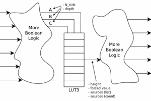
The new logic block is much more capable than the original one. It is basically copied from the design shown on the Wikipedia page for FPGAs. There are four inputs and one output, plus a carry bit in and carry out. The four inputs feed into two 3-input lookup tables, which are selected between by the fourth input (allowing it them to be used a 4-input LUT). There is also a toggle-able full-adder and D-flipflop. Using the full-adder forces the LUTs to behave as two tables with three inputs.
At this point I want to experiment with routing using the MOSIS cell library and verifying the design.
I've added parameterized versions of the routing block and switch block. Both use Verilog's generate statement along with a parameter that determines how many wires come out of each side of the blocks. Interestingly, this runs up against an edge case of Verilog's inout wires. If you create individual wires (i.e. wire w1, w2) to connect modules' inout ports using the unnamed port convention, they can transmit the signal. However if you create an array or vector of wires (i.e. wire [3:0] w) then it breaks. Switching to the named port convention solves that problem.
I've added a testbench that verifies that a switch block can route a signal into and out of a logic block. I was originally writing a testbench that programmed a full adder in the logic cells, but manually configuring memory is tedious and mistake-ridden. I backpedaled and decided to just use one XOR gate, and XOR two signals and send it out the top of the FPGA, but that is still a lot to do. I've included the broken testbench in the repo just in case.
I decided I would release the code under the GPLv3. I'll attach the repository to this page shortly.
The next step is to parameterize the design, which will make it easier to use a more powerful logic cell.
I have created a proof of concept FPGA in Verilog. The architecture overview is the image with the squares. Design choices were made at this stage based on ease of implementation. I started this out of curiosity but then it seemed to work. I'll explain my choices as I go.
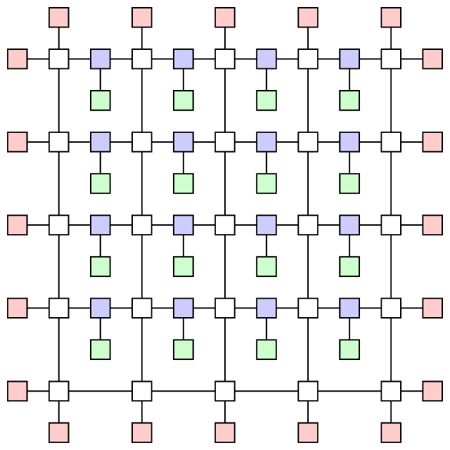
The channels in the routing fabric are three wires wide. Each wire is bidirectional; the direction is selected by configuring the switches in the routing and switch blocks. Originally I used monodirectional wires, but I switched to bidirectional wires after realizing how much monodirectional wires complicate the switch/routing blocks.
All switches in the design are currently based on tristate buffers. Two tristate buffers are wires in anti-parallel, and turning one on and the other off allows the signal to propagate in a particular direction. This is the best I think I can do in vanilla Verilog. Eventually I can use something more area efficient. Generally six of these bidirectional switches are arranged around four wires, to allow them to connect in various ways/directions. Below is a diagram showing the location of the switches.

I chose to use disjoint routing blocks (white squares). They don't allow all possible connections to be made between the ports, but they only need three switches. They were definitely the simplest to implement. Below is a diagram showing the location of the switches within the block, and a diagram showing the possible connections in a disjoint routing block.

The switch blocks (blue squares) are a three by three matrix of switches. These connect the logic cells to the routing fabric. There are no connections at the top, only the bottom (logic cell) and sides (fabric). Below is the diagram of the switch block.

The logic cells (green squares) are very simple right now. They have a four-entry look-up table, a switchable D-flipflop, two inputs, and one output. Each cell can only emulate a two input function (basically a single logic gate). Adding functionality to the cells is not too hard. The only complexity is adding more wires to the fabric when the number of inputs and outputs increases.
The components were connected in rows, then row by row from the bottom up. The IO blocks were wired last.
I tested all of the components in isolation except for the switch block. I also tested the entire FPGA, routing a signal from the bottom to the top. More comprehensive testing is needed. The logic blocks and their integration with the fabric hasn't been tested yet (although they work on their own).
I used Icarus Verilog to compile and test this project. I would like to move to SystemVerilog (for correctness) and/or Verilog A/MS (for features vanilla Verilog can't handle). I am also interested in implementing some kind of heterogenous architecture. Some logic cells can be replaced by DSP or other circuits. As I am a biomedical engineer, I would like to use this project as the basis for medical instrumentation.
There is no code uploaded because I'm still figuring out licensing. I'm not sure what the best license would be.
Thanks for taking a look!
Best,
Will
Go to the Github repository, clone, and build it!
Create an account to leave a comment. Already have an account? Log In.
How is the project going? No commits since '16 june, is it abandoned? :(
Hey there, I still have interest in the project but other things have had my attention.
@Will Long alright, keep us posted! I want to use it in a project of mine, later, at some point.
Excellent! It is very similar to an idea which I have. Will be following your progress with interest
Will Long, your project is awesome!
I am going to read all the information in your git hub and try to understand your verilog code in a few days. Hopefully, I may give you a hand on some work to be done.
Keep it up!
Become a member to follow this project and never miss any updates
 Al Williams
 Yann Guidon / YGDES
How many of your open logic cells can you fit on a real FPGA? It would be interesting to implement fpga-on-fpga, because after you generate your generate a proprietary bitstream for that device, you will be left with a small, but working and 'open' prototype device you can physically interface to. Software emulation of other processors usually take at least a 10:1 hit in speed; I wonder what the factor is with FPGAs. If it's 10:1 speed, 10:1 design size, or both.