Close
0%
0%

FPGA Bootcamp #1

Learn FPGA Design from the ground up with Verilog

Similar projects worth following
FPGAs have been around for awhile. At first, they were expensive and required exotic tools, but that hasn't been the case for awhile. Now they are starting to take off with all designers. Are you ready?

FPGAs are hardly new. But at first they were expensive and required expensive tools and design techniques. That hasn't been true for awhile and FPGAs are now cheap and starting to show up in lots of embedded systems -- even Arduino now has an FPGA/CPU combination. Are you ready for FPGAs? It seems like using an FPGA is like writing software, but it is actually quite different.

There are a few ways people tend to use FPGAs:

1) Replace logic gates like AND and OR gates, flip flops, etc. 

2) Perform algorithms in hardware which can be very parallel either with or without a CPU

3) Provide custom I/O devices for a CPU

4) Build custom CPUs

(You can find more details about how people use FPGAs in the Project Log notes.)

This is part 1 of the bootcamp. You won't need anything special to follow along -- not yet, anyway. We'll use an online simulator that's available for free. You can also use any other Verilog simulator you like, if you'd rather use your own tools.

You should probably know a programming language like C or C++ before attempting this as it isn't a Verilog tutorial per se. Verilog looks a lot like C but it is actually quite different. While C is a language for specifying steps that a CPU takes, Verilog is a language for specifying what you want to happen. For example, if you specify a 7-segment decoder that takes 4 binary bits and lights LED segments in a display, the Verilog tools will realize what you want and build the equivalent hardware for it. That hardware doesn't execute step-by-step. It just "is." 

Think about the light switches in your house. There's nothing saying "let me check the living room switch followed by the bedroom switch followed by the closet..." A CPU would work like that. But in your house -- and in an FPGA -- the switch is just connected to the light so when you flip the switch the light turns on. If you have one switch or 1,000 they all work the same way and take the same small amount of time to operate. Things don't "run" the way they do in a CPU, but just like you can think of all your light switches "running" in parallel , that's how FPGA hardware is.

We will talk about the Lattice IceStick in this tutorial even though we won't use it until a later bootcamp. This is a $26 board that plugs into your USB port and even has open source tools available which we will use.
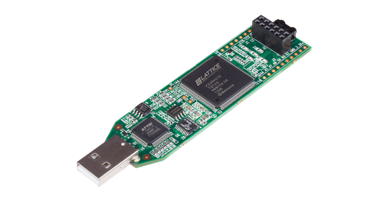
The IceStick has a modest FPGA onboard. From its manual, it has the following features:

  • High-performance, low-power iCE40HX1K FPGA
  • FTDI 2232H USB device allows iCE device programming and UART interface to a PC
  • Vishay TFDU4101 IrDA transceiver
  • Five user LEDs (one green and four red)
  • 2 x 6 position Diligent Pmod compatible connector enables many other peripheral connections
  • Discera 12Mhz MEMS oscillator
  • Micron 32Mbit N25Q32 SPI flash
  • 16 LVCMOS/LVTTL (3.3V) digital I/O connections on 0.1” through-hole connections

The FPGA isn’t huge (1,280 logic cells), but it is big enough to host a simple CPU. We aren’t going to start with a CPU, though. We’ll start with something much more simple.

OK, that's enough for this section. When you are ready, move on to the steps and get started on your FPGA adventure! You'll also find background articles in the project logs. You might want to browse them first and refer back to them as you work through the steps. The logs also have a glossary you can check for any unfamiliar terms.

This tutorial is part of a series:

Bootcamp 0Covers basic digital logic concepts with simulations
Bootcamp 1Introduction to FPGA coding and simulation with combinatorial logic (this bootcamp)
Bootcamp 2More FPGA coding and simulation with flip flops (sequential logic)
Bootcamp 3Working with...
Read more »

testbench.v

The normal testbench. You only need this file if you are not using EDAPlayground as a simulator (since the file is already there).

x-verilog - 500.00 bytes - 06/21/2018 at 22:20

Download

testbench-display.v

Alternate testbench that adds $display statements. This isn't as useful on EDAPlayground (although it does show up in the console), but if you use your own simulator it shows how you can do essentially "printf debugging" in your testbenches.

x-verilog - 710.00 bytes - 06/21/2018 at 22:20

Download

design.v

The actual adder design. You only need this file if you are not using EDAPlayground as a simulator (since the file is already there).

x-verilog - 740.00 bytes - 06/21/2018 at 22:20

Download

  • 1 × Lattice IceStick FPGA board Not actually needed for Bootcamp #1 but you will need it by the end of the series
  • 1 × An account on http://www.edaplayground.com You don't actually need an account, but it will make things nicer. The account is free and if you don't like to hand our your e-mail, use a disposable one
  • 1 × Icarus Verilog Optional. If you don't want to use edaplayground, you can use Icarus or another simulator on your local PC
  • 1 × GTKWave Optional. If you want to use your own simulator you will need this program or another similar program to view the output

  • Why a Half Adder?

    Al Williams07/19/2018 at 21:43 0 comments

    You might wonder why we are building a half adder and what other kinds of adders there are. A half adder takes two bits in and produces two output bits, a sum and a carry:

    ABSumCarry
    0000
    0110
    1010
    1101

    This is suitable for adding the first two bits of a multibit word. The reason you can't use it on subsequent bits is because it lacks an input for a carry bit from the previous stage. You really need a 3-bit adder. One that takes the two input bits and the carry from the previous bit. That's a full adder:

    ABCarry In (C)SumCarry Out
    00000
    00110
    01010
    01101
    10010
    10101
    11001
    11111

    The full adder is almost -- but not quite -- two half adders. Typically, for a full adder you'll need two two-input XOR gates. One computes B+C and the other takes that sum and adds A to produce the final sum. There are several ways to compute the carry, but one way to do it is to realize that the carry out is true in two cases. The first is when A is 1 and B+C (that is, the sum from the first XOR gate) is also 1. That covers the rows above where A=1, B=0, C=1 and A=1, B=1, C=0. That leaves two rows uncovered:  A=0, B=1, C=1 and A=1, B=1, C=1. If you think about it, the A must be a don't care because it can be either a 1 or a 0. So the second case is B=1 and C=1.

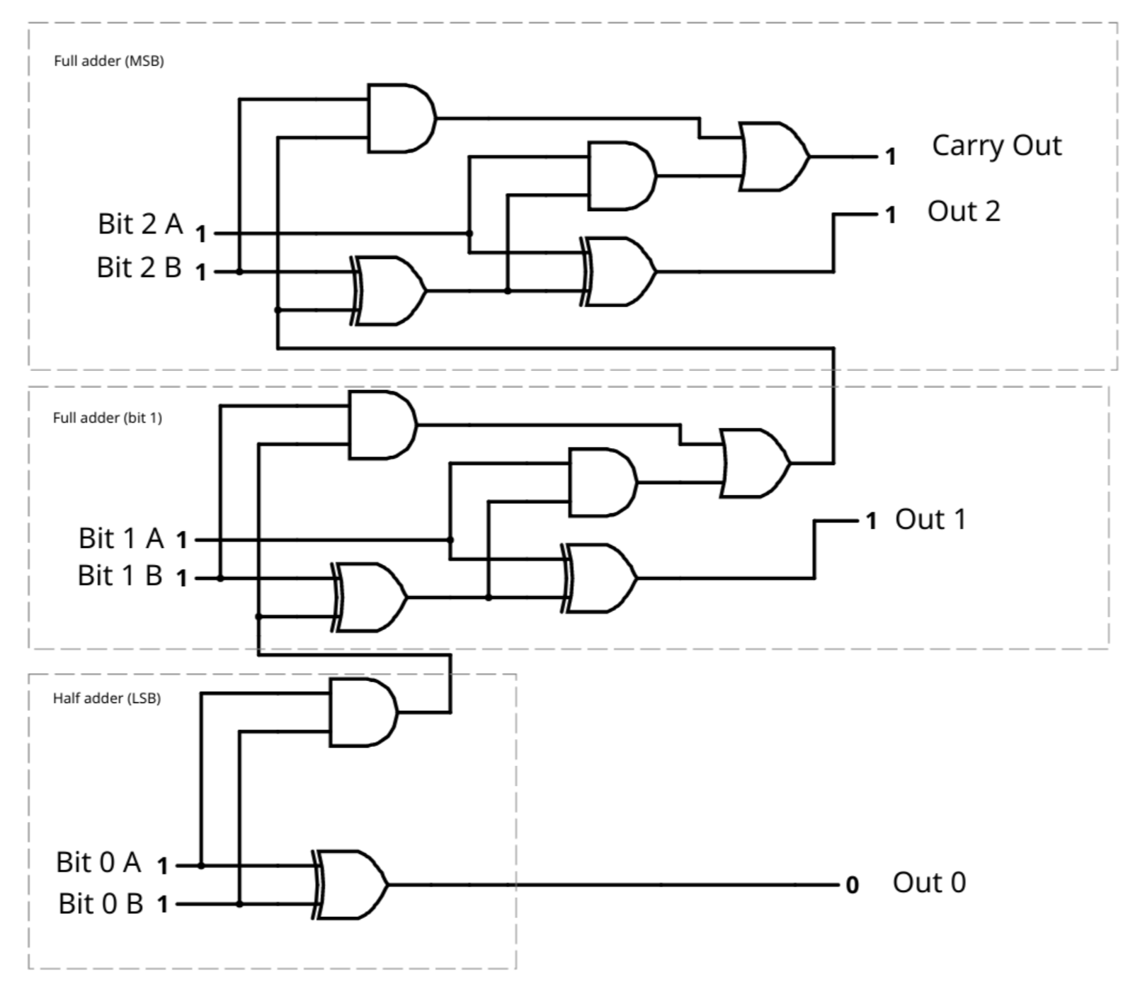
    You can easily implement this with two AND gates and an OR gate. The schematic appears below and if you click the link you can try it in the excellent Falstad simulator (just click on the left side 1s and 0s to set the input you like). The bottom half adder handles the least significant bit (LSB). The carry output goes to the full adder for bit 1 through the carry input. That adder's carry output goes to the most significant bit (MSB) full adder.

    You could implement this in Verilog for practice using gates, but in reality, Verilog will figure this out for you when you write something like:

    module fulladder(output carryout, output [2:0] sum,
                     input [2:0] a, input [2:0] b);
      
      assign {carryout, sum} = a+b;
      endmodule

    Not only is this easier, but the FPGA tools will probably identify how to do this using parts of the FPGA specifically meant for things like carry propagation, allowing you to possibly get higher density and speeds than if you just specified things at a gate level. You can experiment with that in the simulator, if you like.

  • A Quick FPGA Glossary

    Al Williams06/24/2018 at 21:40 0 comments

    • Adder - See Full Adder and Half Adder.
    • AND Gate - A gate who's output is 1 only when all inputs are 1.
    • Blocking assignment - In Verilog, when an assignment occurs before any subsequent assignments (that is, it does not occur in parallel).
    • Combinatorial Logic - Logic that does not rely on the previous state of the system to set the current output state.
    • Exclusive OR Gate - See XOR Gate.
    • Flip Flop - A circuit element that can take one of two states (1 or 0) and remember it until changed. Somewhat like a one-bit memory device.
    • Full Adder - A circuit for adding two binary numbers and a carry bit (so three bits overall). It will produce a sum and a carry.
    • FPGA - Field Programmable Gate Array.
    • Half Adder - A circuit for adding two binary numbers. It will produce a sum and a carry
    • Inverter - See NOT Gate.
    • IP - Intellectual Property. Typically a third party module that does a particular function that you can integrate into your FPGA designs if you wish.
    • Logic Diagram - See Schematic.
    • Non-blocking Assignment - In Verilog, when an assignment occurs in parallel with other assignments in the same block.
    • NOT Gate - A gate that takes a single input and inverts it. That is, a 1 becomes a 0 and a 0 becomes a 1.
    • OR Gate - A gate who's output is a 1 if any inputs are 1.
    • Schematic - A diagram of a logic circuit  made up, usually, of logic symbols for fundamental gates.
    • Sequential Logic - Logic that typically uses flip flops and the current output state influences future output states.
    • Testbench - Verilog (or similar) code that exists only to send stimulus to a simulated device and record or test the results.
    • Truth Table - A table showing a logic circuit's possible inputs and the outputs that will result.
    • Workflow - The process of taking design inputs and producing a working FPGA configuration.
    • Verilog - A description language used to describe logic you wish to place on an FPGA.
    • VHDL - A description language (not used in this bootcamp) to describe logic you wish to place on an FPGA.
    • XOR Gate - Exclusive OR gate. A two-input gate that sets its output to 1 if either input is a 1, but not when both inputs are a 1.

    Logic Truth Tables for Two-Input Gates

    ABANDORXOR
    00000
    01011
    10011
    11110

  • How People Use FPGAs

    Al Williams06/24/2018 at 19:54 0 comments

    There are a few ways people tend to use FPGAs:

    1) Replace logic gates like AND and OR gates, flip flops, etc. 

    2) Perform algorithms in hardware which can be very parallel either with or without a CPU

    3) Provide custom I/O devices for a CPU

    4) Build custom CPUs

    You might think that these are all just applications of #1 and to some extent you'd be right. However, in many cases people use "Intellectual Property" or IP to build up algorithms, custom CPUs, or custom I/O devices without actually worrying about the details. Just like you can use someone's C library in your Visual Basic Program even if you don't need C, IP lets designers share functions with people who might not be able to build them themselves. We won't talk much about that because we want to design!

    Another trend is to see FPGAs married with CPUs either on the same board or, in some cases, in the same package. Sometimes, the FPGA has an actual CPU hardwired into the silicon. In other cases, the CPU is "soft" and just consumes some of the resources available to you as an FPGA designer.

    A lot of example FPGA projects don't really show the best uses of FPGAs. For example, a fair beginner project might be a simple traffic light with some red, green, and yellow LEDs. But the reality is there is no advantage to using an FPGA for this over a processor. The time scale is relatively long and doesn't need high precision. FPGAs are harder to work with and often take more power than a stand-alone CPU. So you really want to use them where there is a compelling advantage.

    For example, suppose you have an industrial process that if any limit switch hits you need to stop immediately. Further, for whatever reason, every switch needs to be separate. So if you have 10 switches you are going to have 10 inputs.

    On a CPU, the simple way to do it would be to test each switch in turn. But that's going to be slow because you have to look at switch 1, then switch 2, and so on. Presumably, the CPU is also doing something else.

    Another idea would be to get all 10 inputs into a 16-bit word, for example, and test that. That's better, but still doesn't solve the problem of you have to do other things and while you are doing those things, you aren't watching the switches. You'd probably want to make each switch generate an interrupt (or OR them together and use that as an interrupt). That's better, but there are still times when an interrupt won't occur right away, so the timing won't be great. 

    Now what if you have 50 inputs? Your timing is probably going to be worse. With an FPGA, you could make each input trigger circuitry and while it won't be instant, it won't matter significantly if you have 10 or 50 inputs. At some point you'll run out of pins, but until then, it won't matter.

    In effect, all the switches "run" in parallel. This is useful for processing audio or video, too. Say you have audio buffered at 22 kHz for one second. That's 22,000 samples. You need to do some math operation. A common CPU will do one at a time. If you have threads, you might be able to pretend to do more. Some CPUs have special instructions made to do things in parallel, but maybe not 22,000 at once. With an FPGA of the right size, you could define the math block for one sample, duplicate it 22,000 times and -- with the right memory architecture -- do the processing in what amounts to a blink of time.

    So for learning, it doesn't really matter. But in the real world, you want to pick the right tool for the job. FPGAs aren't for everything. But when you need their inherent parallelism, they can be the best -- and most practical -- choice.

  • Verilog?

    Al Williams06/22/2018 at 21:52 0 comments

    Verilog is one way to do design entry -- the process of telling the FPGA tools what you want the FPGA to do. Just like software might be in C or Python or Java, there are many ways to do design entry. It is often possible to use schematics -- really logic diagrams -- to define an FPGA, but there's good reasons why that doesn't work as well on larger projects that we will talk about in this bootcamp.

    However, you will many people use VHDL which is very similar in concept to Verilog. However, where Verilog is somewhat similar to C, VHDL is very similar to Ada. There are other options, as well. There are tools that will convert limited subsets of the C language to FPGA configurations, for example. There's also System Verilog which has a lot of additional features, most of which are aimed at simulation.

    There are also lesser-used languages. Some are proprietary and have mostly fallen out of use. Some are newcomers that usually look somewhat like another programming language. SpinalHDL and MyHDL are examples. The purpose of all of these things are the same: to inform the FPGA configuration tool what it is you want.

    Obviously, not all tools are going to take all languages. However, if a toolset can handle, for example, Verilog and VHDL, you can probably mix these if you want in one project. That may seem crazy, but it is a great benefit if you have libraries or functions from a third party in one language and you want to use another one.

    This is usually possible because there is a fairly standard intermediate format called EDIF. If you buy IP (intellectual property) from a vendor, it will probably come as an EDIF file. That means you won't be able to easily edit it, but you can add into your designs.

    The tools we are going to use with the IceStick just do Verilog. But if you use commercial tools, you'll likely have an easy time using at least VHDL or Verilog, if you choose. However, this series of bootcamps is going to focus on Verilog.

  • FPGA Timing

    Al Williams06/22/2018 at 06:12 0 comments

    We will have a lot more to talk about for timing in future bootcamps. But I wanted you to think about the speed things operate at. FPGAs usually have a speed rating and the tools have great models of how long a signal will take to propagate from point A to point B at a certain temperature.

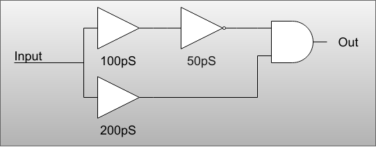
    For simple combinatorial logic like we have in this bootcamp, it won't matter much. The delay through the gates are going to be VERY short (like picosecond-range). However, complex circuits can have issues. Consider a case where a gate takes two inputs. A change on the FPGAs inputs goes through some logic and hits our target gate in 150pS. The other input sees the same outside input change but takes 200pS to do its work.

    That means for 50pS the output could be wrong. For example, suppose the circuit were perfect. Because the two inputs of the AND gate are inverse of each other, the output must always be a zero. However, if the input were high for a long time and then switched to low, the top input to the and gate would change in 150pS. The bottom input is still high for another 50pS before the change registers. During that time, the AND gate could put out a high. The truth is, it won't change state instantly, so it may not go high for the entire 50pS.

    This is sometimes known as a glitch. The more gates between point A and point B, in general, the longer it is going to take. Sometimes, too, a long routing path will cause a longer delay. You may think this is a dumb example because the output shouldn't be able to change. That's true but I wanted to make a point. Besides, you often see this exact circuit used to detect an edge which takes advantage of the glitch. However, you should NOT try to implement something like this in an FPGA. Instead, just think of the buffers as representing some number of arbitrary gates for the purposes of this example. Exactly what it doesn't isn't important.

    We will learn a way around this problem in the next bootcamp (with sequential logic). However, that will cause timing problems of its own and we will have to learn how to work through those as well.

  • FPGA Workflow

    Al Williams06/21/2018 at 23:00 0 comments

    Exactly how you "program" the actual FPGA hardware depends on which chip and vendor you are using. In the bootcamp where we actually program the IceStick, you'll see more details about exactly how to do it. However, most FPGA "builds" follow a very similar flow and you might find it interesting to know what that is.

    If you think about a conventional C program, your workflow looks like this:
    1. Compile C code to object code
    2. Link object code and libraries to executable
    3. Debug executable using simulation
    4. Prepare executable for downloading
    5. Send executable to target system
    6. Debug executable on target system

    The details vary, but a generic FPGA workflow looks like this:

    1. Synthesize Verilog into low-level constructs
    2. Simulate/test/debug system behavior
    3. Map low-level constructs to specific device blocks
    4. Place and route blocks -- this means to plan which blocks go where and exactly how to interconnect them
    5. High-fidelity simulate/test/debug on actual device-specific configuration
    6. Program configuration to FPGA or configuration device
    7. In circuit test/debug, if necessary

    Some vendors use different terms for things like blocks or place and route, but the ideas are universal.

    You might wonder why you would test and debug at three different stages. The simulation in step 2 is like we are doing in this bootcamp. You deal with the source code, things work pretty fast, and you can catch logic errors in your design.

    What you can't catch is problems caused by how things are set up on the chip. Maybe this signal arrives just a little too late and causes an error. The device-specific simulation in step 5 can catch that. But it is generally a lot more data to process and model so the simulations take more time and memory. On a big design it can also be costly to have to go fix source code and then re synthesize. So you try to catch your logic errors in the second step.

    Of course, nothing works exactly like it does in simulation so sometimes you have to debug on the chip. Modern chips have tools to help you see inside them just like modern CPUs have on chip debugging support. But it is still harder and more time consuming.

  • Thoughts on FPGAs

    Al Williams06/21/2018 at 22:50 0 comments

    When you were a kid, did you ever see one of those 100-in-1 electronic kits? These were a board with a bunch of parts on them and some kind of solderless terminal. If you hooked wires up one way it was a car alarm. If you hooked it up another way it was a metal detector. A third way made an AM radio. 

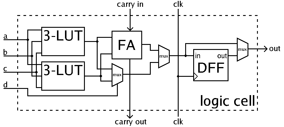
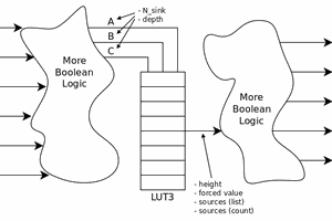
    That's a lot like what an FPGA is. There are a bunch of blocks of functions waiting for you to wire them up. Usually, most of the blocks are exactly the same and there will just be a few special blocks, although some FPGAs will have a significant number of different block types. Exactly what each of these blocks do depends on the FPGA but luckily the tools shield us from most of this complexity. For example, there might be a block that is a look up table (LUT) that holds a truth table that converts, say, 4 inputs to 1 output. That LUT might be grouped together with a flip flop or two and some programmable inverters. Other blocks might provide RAM memory, DSP functions, or clock generation circuits. But almost always the tools will take your Verilog and figure out how to wire up the blocks to build your circuit. As an example, here's a typical FPGA cell:

    The LUTs are look up tables with 3 inputs. The FA is a full binary adder (just like the one we are using in this bootcamp, except it takes a carry in as well as an A and B input). The muxes are electronic switches. The output can be either of the two inputs based on either an input (like d for the leftmost mux) or by configuration for the other two muxes. The block marked DFF is a flip flop and we'll talk about those more in a future bootcamp.

    So if you had this cell and our Verilog from this bootcamp, the tool would probably route a and b to our A and B inputs. It should be smart enough to make the LUTs just forward those bits to the full adder. The output of the full adder would route through both muxes to the output. And the carry out would be routed to our other output.

    It is interesting that fundamentally an FPGA is a memory device. Instead of storing numbers, though, it stores "wires" continuing the kit analogy. Some of those wires select options (like use inverted X as the first input) and some wires connect inputs to outputs. Some FPGAs are based on RAM and need to be loaded every time they power up. That load could come from a CPU or a dedicated memory chip (usually a serial EEPROM). Some devices have a configuration EEPROM onboard. You can probably load the device from a PC using the development tools, also. But if you do, remember the next power cycle won't bring back your "code" -- you'll have to program the EEPROM device for that. Looking at the figure above, each LUT has 8 bits (3 input bits can take a value from 0 to 7). The two muxes furthest to the right are configured so that's one bit each. In addition, there will be bits to select where all the pins entering or leaving the block actually go. This can vary depending on the actual FPGA, but in general all the logic can be placed on one of many local or global busses. The clock signal (clk) probably has its own busses that is separate.

    Other FPGAs are based on nonvolatile memory cells. You can program these and they stick. That's handy at development time, but there is some limit to how many times you can program them, just like flash memory. That limit is pretty high though. One advantage to the FPGAs that stay programmed is they are general ready to operate immediately when the circuit powers on. If the FPGA has to read a configuration from a host computer or a EEPROM it is going to take some time and usually the I/O pins are idle during that time. You have to take care to design around this and also your design has to be able to tolerate that reset time on every power cycle (or even a reset, typically).

    It is an advanced technique, but it is possible to reprogram only parts of the FPGA on the fly. For example, a system with a CPU could use an FPGA to provide many PWM outputs and DSP algorithm....

    Read more »

View all 7 project logs

  • 1
    ▇▇▇▇ Choose Your Simulator ▇▇▇▇

    (Note: the first few steps are more background information. We'll let you know when we shift to building the actual demo project).

    We are going to work in Verilog. You will eventually need two things: a simulator so you can test your work and a translator that can convert the Verilog into something your FPGA can use.

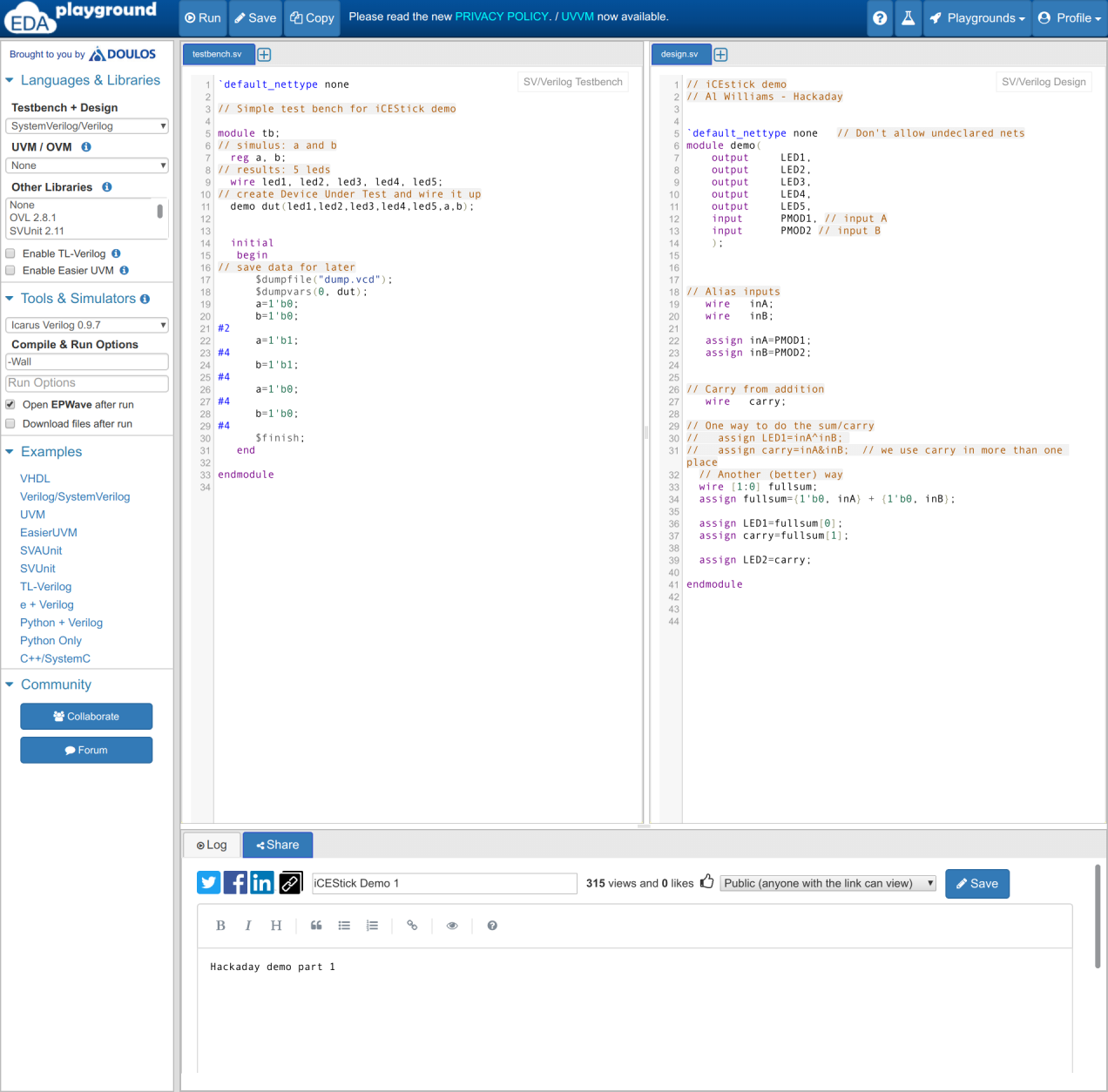
    For this bootcamp you only need the simulator.  I’m going to use EDAPlayground because it is free and it will run in your browser. No software to set up and no worry about your operating system being compatible. If you have a modern browser, you are all set.

    I know some people don’t want to work on the Web or don’t want to create an account (honestly, though, this will just be tutorial code and making up a disposable e-mail address is easy enough). If you just can’t bear it, you can run all the examples on your desktop with Icarus Verilog (using GTKWave to display the results). I just won’t be talking about how to do that except briefly as an option in the very last step. You can read the Icarus introduction if you want to go that route. I still suggest you stick with EDAPlayground for the tutorial.

  • 2
    ▇▇▇▇ Consider Drawing a Schematic ▇▇▇▇

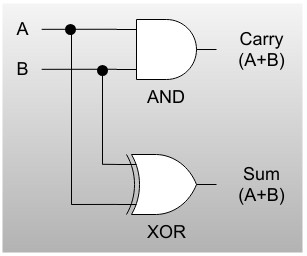
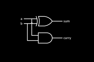
    This is the adder we are going to build. In this case, the schematic is quite clear and easy to figure out. The AND gate's output is only 1 if both inputs are 1. The XOR (exclusive or) gate's output is a 1 if either input is a 1, but not both. If you haven't seen an adder before, consider the truth table (and note the Sum column is the truth table for an XOR gate, while the Carry column is for an AND gate):

    ABSumCarry
    0000
    0110
    1010
    1101

    This is an example of a combinatorial circuit because it contains no flip flops. The past state of the circuit doesn't matter. All you need to know is the inputs and you can figure out what the output is. The other type of circuit -- we will do these later -- is a sequential circuit where the past state might change things. 

    For example, a circuit that lets you push a single button and switch an LED from on to off and then press again to go from off to on would be sequential because it "knows" the state of the LED.

    Just about all FPGAs have software you can use to draw a schematic like this and it will figure it out from there. So that's it, right? Why bother with anything else? 

    Turns out there's good reasons for this.

    After you move away from simple things, the schematics can be very painful. For example, think of a seven segment decoder. If you took a few minutes you could probably work out the AND OR and NOT gates required to perform the function (that is, convert a four-bit binary number to a seven segment display). But it would take a few minutes. If you want an idea of the complexity of that schematic, check out this TI/Harris data sheet.

    If you use Verilog, you can take a simple approach and just write out the gates you want. That will work, but it is usually not the right answer. Instead, you should describe the circuit behavior you want and the Verilog compiler will infer what circuits it takes to create what you need. For the seven segment decoder this could be as simple as:

    always @(*)
    case (number)
     4'h0: dispoutput <= 7'b1111110;  // all segments but center
     4'h1: dispoutput <= 7'b0110000;  // two segments to form "1"
     4'h2: dispoutput <= 7'b1101101;  // five segments to form "2"
     . . .

    Let’s look at that in a little more detail. The always statement tells Verilog that the code following should execute whenever any of the inputs you use in it change. This infers a combinatorial circuit since there is no clock. The case statement is like a switch statement in C. The funny looking numbers are four bit hex (4’h1) and 7 bit binary (7’b1101101). So the code instructs the FPGA (or, more accurately, instructs the Verilog compiler to produce hardware on the FPGA) to examine the number and set dispoutput based on the input.

    The <= character, by the way, indicates a non-blocking assignment. You could also use an equal sign here to create a blocking assignment. For now, the difference doesn’t matter, but we’ll revisit that topic when working with a sequential design.

    From this description of what you want, the Verilog compiler will infer the right gates and may even be able to perform some optimizations. A key difference between an FPGA and building things on a microcontroller has to do with parallelism. If you wrote similar C code on, say, an Arduino, every copy of it would take some execution time. If you had, for example, 50 decoders, the CPU would have to service each one in turn. On the FPGA you’d just get 50 copies of the same circuit, all operating at once.

  • 3
    ▇▇▇▇ Key Point #1: Does Verilog Execute Like Software? ▇▇▇▇

    (Note: now we are going to start working on the Adder. You can download the source from the file section or follow along in the online simulator). 

    Verilog isn't executable in the same way that C or Python code is (except when it is).  That’s a really important point. With an FPGA, the circuitry that drives each part of the 7-segment display (from the last section) just works all the time. Sure, there is a small delay through the gates (probably picoseconds) but that’s true even with discrete circuitry. The delay isn’t because the FPGA is executing lines of Verilog code or some equivalent structure like a CPU executes a C program. The Verilog becomes connecting wires that wire up circuit elements just as though you had a sea of gates on a PCB and you connected them with wire wrap.

    There is an exception to this. During simulation, Verilog does act like a programming language, but it has very specific rules for keeping the timing the same as it will be on the FPGA. However, it also allows you to write constructs that would not be transferable to the FPGA. For example, a subroutine call doesn’t make sense in hardware, but you can do it during simulation. In general, you want to avoid non-synthesizable Verilog except when writing your testbench (the driver for your simulation; I’ll talk more about it in a minute).

    Look back at the adder schematic in the previous step. The sum is a simple XOR gate and the carry is an AND gate. I can express that in Verilog, if I want to, like this:

    assign carry=inA&inB;  // & - and
    assign sum=inA^inB;    // ^ - xor

    It is smarter, though, to let Verilog figure that out. I can make a variable with two bits in it like this:

    reg [1:0] fullsum;

     Then I could say:

    assign fullsum={1’b0, inA} + {1’b0, inB};
    assign carry=fullsum[1];
    assign sum=fullsum[0];

    The braces turn the one bit wires inA and inB into two bit quantities. In this simple example, I might have actually stuck to the first method, but if you think back on the 7 segment decoder, you’ll see it makes sense to use this inferring style where possible.

    If you need more help with the Verilog language, you might consider visiting the tutorials from Doulos -- the same people who host EDA Playground. Here's another self-study Verilog course that's worth checking out.

View all 9 instructions

Enjoy this project?

Share

Discussions

Similar Projects

Does this project spark your interest?

Become a member to follow this project and never miss any updates