-
1▇▇▇▇ Choose Your Simulator ▇▇▇▇
(Note: the first few steps are more background information. We'll let you know when we shift to building the actual demo project).
![]()
We are going to work in Verilog. You will eventually need two things: a simulator so you can test your work and a translator that can convert the Verilog into something your FPGA can use.
For this bootcamp you only need the simulator. I’m going to use EDAPlayground because it is free and it will run in your browser. No software to set up and no worry about your operating system being compatible. If you have a modern browser, you are all set.
I know some people don’t want to work on the Web or don’t want to create an account (honestly, though, this will just be tutorial code and making up a disposable e-mail address is easy enough). If you just can’t bear it, you can run all the examples on your desktop with Icarus Verilog (using GTKWave to display the results). I just won’t be talking about how to do that except briefly as an option in the very last step. You can read the Icarus introduction if you want to go that route. I still suggest you stick with EDAPlayground for the tutorial.
-
2▇▇▇▇ Consider Drawing a Schematic ▇▇▇▇
![]()
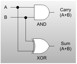
This is the adder we are going to build. In this case, the schematic is quite clear and easy to figure out. The AND gate's output is only 1 if both inputs are 1. The XOR (exclusive or) gate's output is a 1 if either input is a 1, but not both. If you haven't seen an adder before, consider the truth table (and note the Sum column is the truth table for an XOR gate, while the Carry column is for an AND gate):
A B Sum Carry 0 0 0 0 0 1 1 0 1 0 1 0 1 1 0 1 This is an example of a combinatorial circuit because it contains no flip flops. The past state of the circuit doesn't matter. All you need to know is the inputs and you can figure out what the output is. The other type of circuit -- we will do these later -- is a sequential circuit where the past state might change things.
For example, a circuit that lets you push a single button and switch an LED from on to off and then press again to go from off to on would be sequential because it "knows" the state of the LED.
Just about all FPGAs have software you can use to draw a schematic like this and it will figure it out from there. So that's it, right? Why bother with anything else?
Turns out there's good reasons for this.
After you move away from simple things, the schematics can be very painful. For example, think of a seven segment decoder. If you took a few minutes you could probably work out the AND OR and NOT gates required to perform the function (that is, convert a four-bit binary number to a seven segment display). But it would take a few minutes. If you want an idea of the complexity of that schematic, check out this TI/Harris data sheet.
If you use Verilog, you can take a simple approach and just write out the gates you want. That will work, but it is usually not the right answer. Instead, you should describe the circuit behavior you want and the Verilog compiler will infer what circuits it takes to create what you need. For the seven segment decoder this could be as simple as:
always @(*)
case (number)
 4'h0: dispoutput <= 7'b1111110;  // all segments but center
 4'h1: dispoutput <= 7'b0110000;  // two segments to form "1"
 4'h2: dispoutput <= 7'b1101101;  // five segments to form "2"
 . . .
Let’s look at that in a little more detail. The
alwaysstatement tells Verilog that the code following should execute whenever any of the inputs you use in it change. This infers a combinatorial circuit since there is no clock. Thecasestatement is like aswitchstatement in C. The funny looking numbers are four bit hex (4’h1) and 7 bit binary (7’b1101101). So the code instructs the FPGA (or, more accurately, instructs the Verilog compiler to produce hardware on the FPGA) to examine the number and setdispoutputbased on the input.The
<=character, by the way, indicates a non-blocking assignment. You could also use an equal sign here to create a blocking assignment. For now, the difference doesn’t matter, but we’ll revisit that topic when working with a sequential design.From this description of what you want, the Verilog compiler will infer the right gates and may even be able to perform some optimizations. A key difference between an FPGA and building things on a microcontroller has to do with parallelism. If you wrote similar C code on, say, an Arduino, every copy of it would take some execution time. If you had, for example, 50 decoders, the CPU would have to service each one in turn. On the FPGA you’d just get 50 copies of the same circuit, all operating at once.
-
3▇▇▇▇ Key Point #1: Does Verilog Execute Like Software? ▇▇▇▇
(Note: now we are going to start working on the Adder. You can download the source from the file section or follow along in the online simulator).
Verilog isn't executable in the same way that C or Python code is (except when it is). That’s a really important point. With an FPGA, the circuitry that drives each part of the 7-segment display (from the last section) just works all the time. Sure, there is a small delay through the gates (probably picoseconds) but that’s true even with discrete circuitry. The delay isn’t because the FPGA is executing lines of Verilog code or some equivalent structure like a CPU executes a C program. The Verilog becomes connecting wires that wire up circuit elements just as though you had a sea of gates on a PCB and you connected them with wire wrap.
There is an exception to this. During simulation, Verilog does act like a programming language, but it has very specific rules for keeping the timing the same as it will be on the FPGA. However, it also allows you to write constructs that would not be transferable to the FPGA. For example, a subroutine call doesn’t make sense in hardware, but you can do it during simulation. In general, you want to avoid non-synthesizable Verilog except when writing your testbench (the driver for your simulation; I’ll talk more about it in a minute).
Look back at the adder schematic in the previous step. The sum is a simple
XORgate and the carry is anANDgate. I can express that in Verilog, if I want to, like this:assign carry=inA&inB; // & - and assign sum=inA^inB; // ^ - xor
It is smarter, though, to let Verilog figure that out. I can make a variable with two bits in it like this:
reg [1:0] fullsum;
Then I could say:
assign fullsum={1’b0, inA} + {1’b0, inB};
assign carry=fullsum[1];
assign sum=fullsum[0];
The braces turn the one bit wires
inAandinBinto two bit quantities. In this simple example, I might have actually stuck to the first method, but if you think back on the 7 segment decoder, you’ll see it makes sense to use this inferring style where possible.If you need more help with the Verilog language, you might consider visiting the tutorials from Doulos -- the same people who host EDA Playground. Here's another self-study Verilog course that's worth checking out.
-
4▇▇▇▇ Modules and Definitions ▇▇▇▇
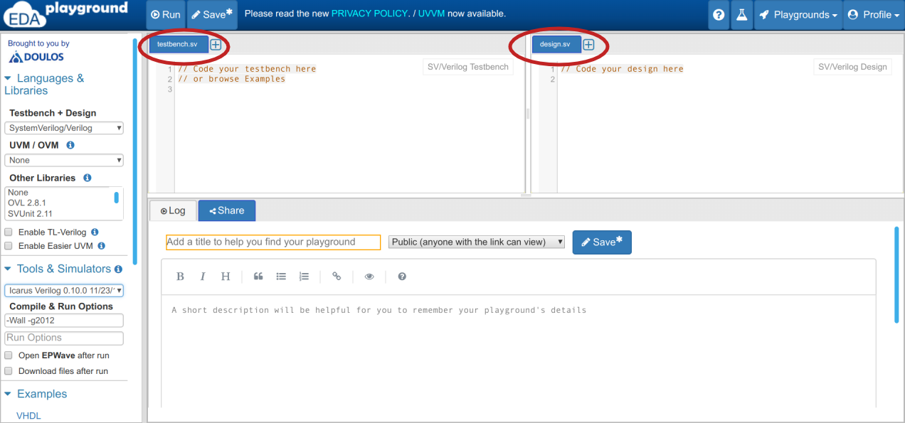
When you first open EDA Playground, you will see an editor window with two documents open. One is testbench.sv and one is design.sv -- the SV is for "SystemVerilog" although we will only be using the Verilog features.
![]()
Look on the left hand side of the screen an make sure you have the settings as seen above. In general, you'll only need to set the Testbench+Design to SystemVerilog/Verilog and the Tools & Simulators section to Icarus Verilog 0.10.0 11/23/14 or Icarus Verilog 0.9.7. Probably any other Verilog simulator would work, too. You can leave the Compile & Run options set to whatever the default for the tool you pick is. Also, make sure Open EPWave after run is checked (it is not checked in the screenshot above).
![]()
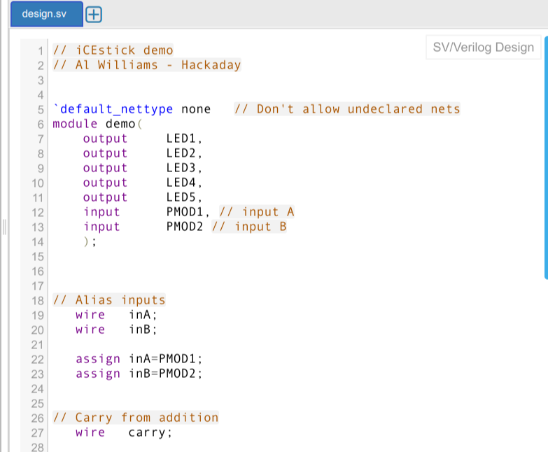
If you browse the source code, you’ll notice there’s a few minor things I glossed over. For one, all of this code lives in a module. You can think of a module loosely as a subroutine or, better, a C++ class. Other modules can create copies of a module and map different signals to its inputs and outputs. There’s also definitions of all the nets used (we already talked about wires and regs):
module demo(
 output LED1,
 output LED2,
 output LED3,
 output LED4,
 output LED5,
 input PMOD1, // input A
 input PMOD2, // input B
 input PMOD3, // run/stop
 input PMOD4 // reset
 );

// Alias inputs
 wire inA;
 wire inB;
 assign inA=PMOD1;
 assign inB=PMOD2;
Note that I wanted the signals to have names associated with the physical hardware (like
LED1andPMOD2) but then later I wanted to use more meaningful names likeinB. Theassignstatement makes this connection. This is a simple use of that statement. If you recall, one way to build the adder was to assign two bits using an expression. That kind of usage is far more common.If you want to follow along, take the design.v or design.sv file from the Files section and paste it into the design.sv window. You'll wind up with something like this (keep in mind, there's more to the file you'd have to scroll to see):
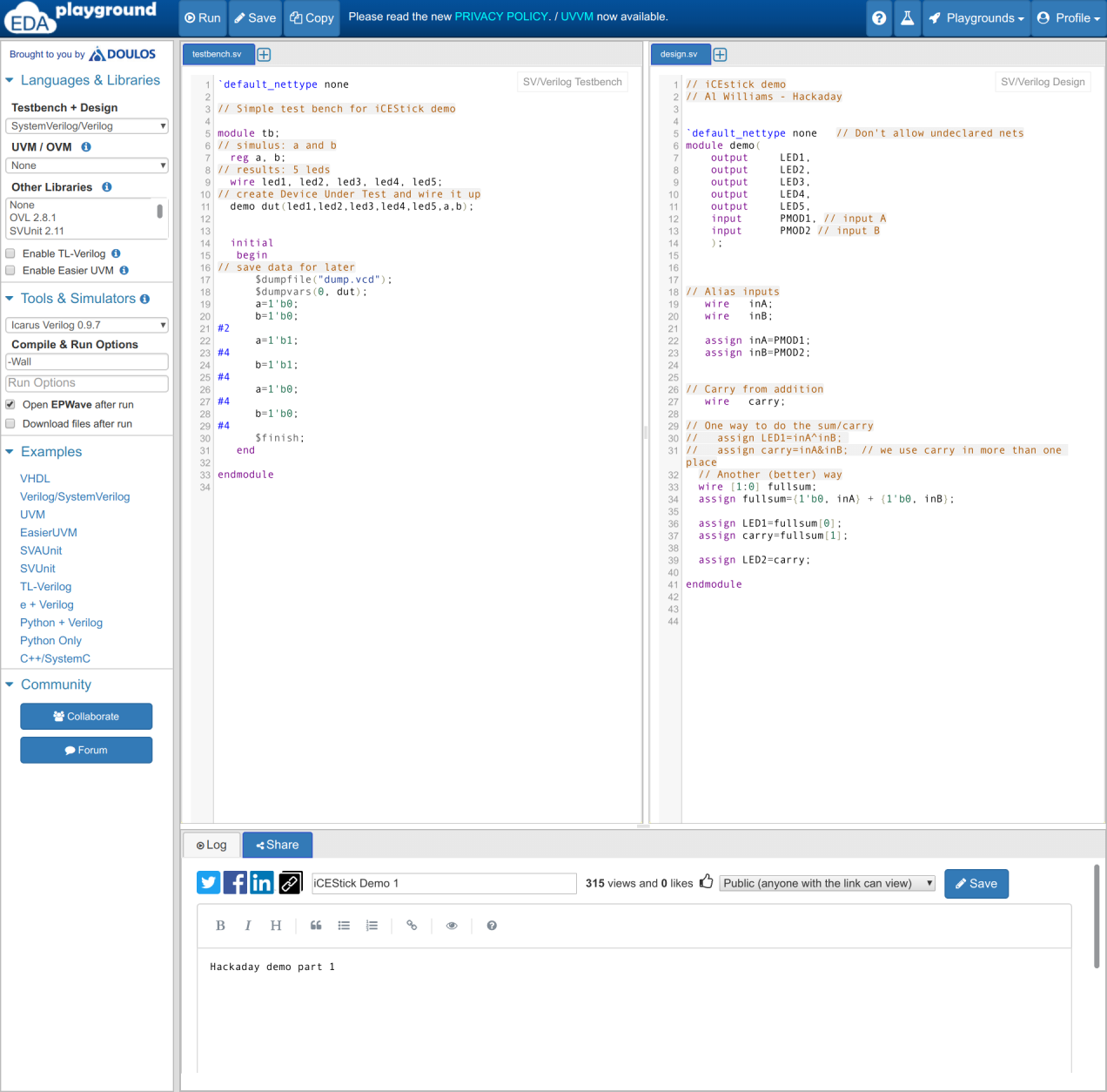
![]()
-
5▇▇▇▇ Create a Testbench ▇▇▇▇
Before you commit your design to an FPGA, you’ll probably want to simulate it. Debugging is much easier during simulation because you can examine everything. When the Verilog simulator runs, it follows rules about timing that take into account how everything runs at the same time, so the behavior should be exactly what your FPGA will do.
The only thing many simulators won’t do is account for things like timing on the chip itself (although with the right tools, you can simulate that too). For example, your design may depend on an input changing before a clock edge (the set up time on the flip flop, for example) but because of the routing on the chip, the input won’t change in time.
This kind of timing violation is a real problem with large chips and high speeds. For this sort of small circuit, it shouldn’t be an issue. For now, we can assume if the simulation works, the FPGA should behave in the same way.
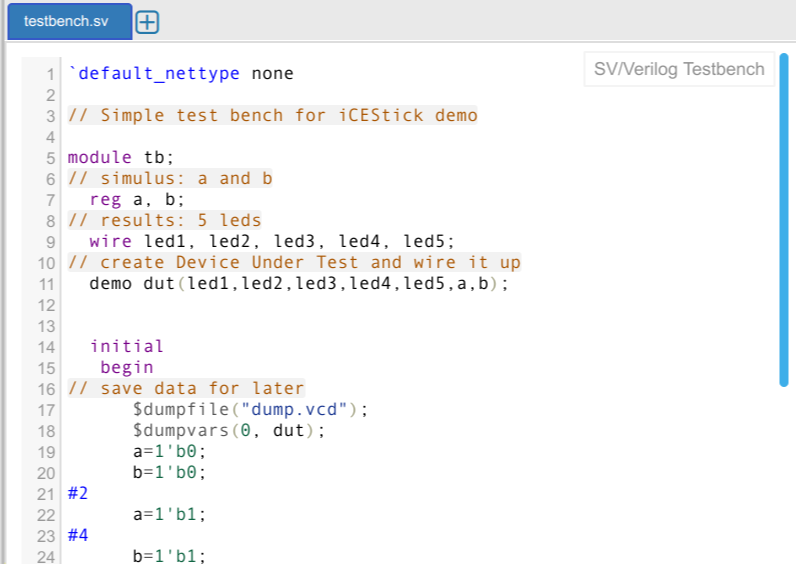
If you are following along, take the testbench.v or testbench.sv file from the Files section or the simulator and paste it into the testbench.sv window. It should look like this (remembering that there's more to the file if you scroll):
![]()
To test our code, we need a testbench which is just a way to say a piece of Verilog code that works like the outside world to our unit under test (in this case, the whole design). The code will never synthesize, so we can use strange Verilog features that we don’t normally use in our regular code.
The first thing to do is create a module for the testbench (the name isn’t important) and create an instance of the module we want to test:
`default_nettype none
module tb;
 reg  a, b;
 wire led1, led2, led3, led4, led5;
 demo dut(led1,led2,led3,led4,led5,a,b);
Note that there is a
regfor each input we want to feed the device under test and awirefor each output it will drive. That means all of thoseregvariables need to be set up to our test conditions.The variables need to be initialized. Verilog provides an initial block that is usually not valid for synthesis, but will be the main part of most test benches. Here’s the first part of it:
 initial
 begin
   $dumpfile("dump.vcd");
   $dumpvars(0, dut);
   a=1'b0;
   b=1'b0;
The two $ statements tell the testbench to dump variables from the device under test to a file called dump.vcd (this is where EDAPlayground looks for it, too, so don’t change it unless you are using your own Verilog simulator). We’ll be able to examine anything that gets dumped. You can also print things using $display, but with EDAPlayground, the dumps are more useful. You can see an example of the testbench with some simple display statements in the file download area. Note that none of these $ statements will work on the FPGA. They are just for simulation.
The next thing you need is some test case stimulus for the adder to -- well -- add:
#2
 a=1'b1;
 #4
 b=1'b1;
 #4
 a=1'b0;
 #4
 b=1'b0;
 #4
 $finish;
 end
So at first, a=1 and b=0. Then after 4 cycles, a=1 and b=1. After another 4 cycles a=0, b=1. Then a=0, b=0. The $finish statement causes the simulation to end. Without this, the clock generator will cause the simulation to keep going forever.
In the end you will wind up with this stimulus in the waveform viewer:
![]()
In the next step, you'll see how to get the rest of the waveforms -- that is, the outputs!
-
6▇▇▇▇ Run Simulation! ▇▇▇▇
You can find the code and the testbench on EDAPlayground (you can even run the simulation from there). When you run the simulation, a waveform will appear (see below). If you want to know more about how it works, check out the video below and I’ll walk through it step by step.
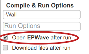
If you are impatient, just press Save followed by Run. You should get the trace window which we will look at in the next section. If not, make sure you have "Open EPWave after run" checked on the left hand side (second picture, below).
![]()
If you don't get the popup window, be sure you have the right options selected (see below). You might also check to see if you have popups blocked in your browser.
![]()
Note: the video may use a different Verilog simulator, but since we are using standard Verilog features, it should not make any difference.
-
7▇▇▇▇ View Results ▇▇▇▇
![]()
Your waveform view window should look about like the above. Notice, it pops up in a new window or tab so your original work is still where you left it. However, if you run again, the EPWave viewer will replace the old waveform, you won't get multiple ones.
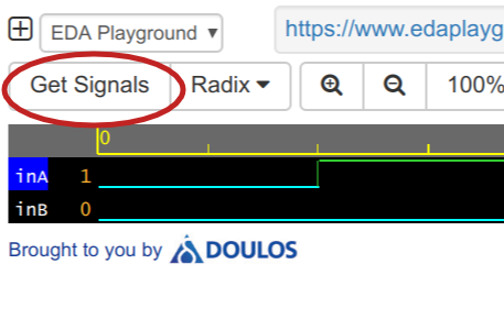
Initially, all you can see is the inA and inB signals -- the input stimulus to the testbench and depending on a variety of factors, you may not even see those. There is a bar of controls at the top. The magnifying glasses and percentage allow you to zoom in or out while the left and right arrows scroll (region 1 in the picture below).
![]()
If you click on one of the waveforms, you can use the button after the left and right arrows (2) to jump back to the time you clicked on (which will look like a vertical line in the graph; see 3). The up and down arrows (4) will select a different trace, and the X button (5) will remove the trace. You can also see, next to the X button (at location 6), what trace you have selected, if any.
Of course, what you really want is to view the output of the simulation. Press Get Signals.
![]()
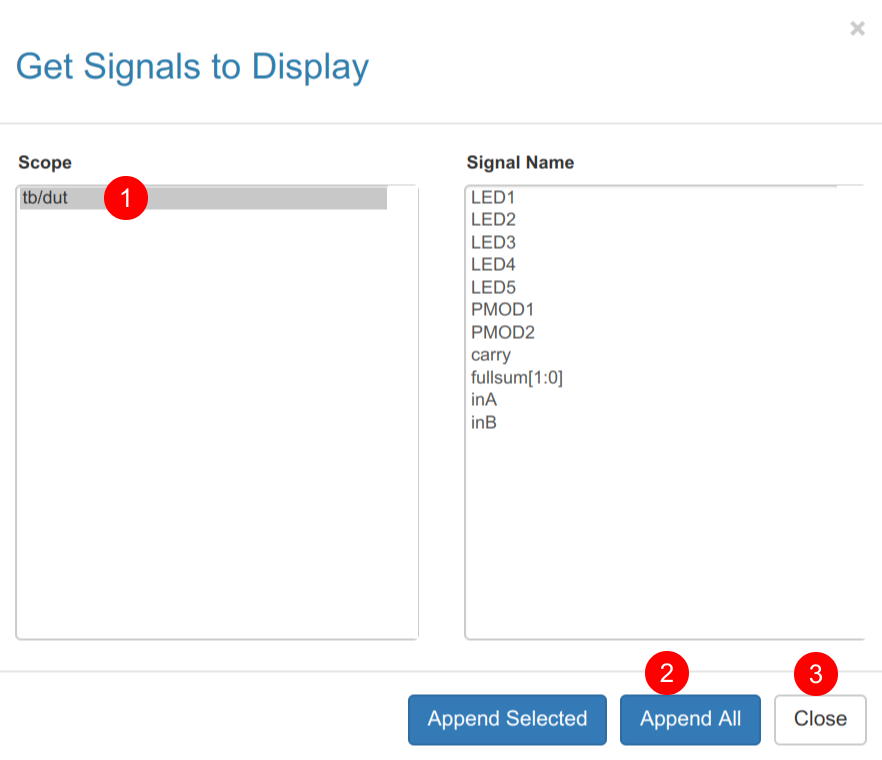
A dialog will appear with two parts: Scope and Signal Name. Right now, the Scope box will only have one entry: tb/dut which is the device under test in our testbench. The Signal Name box will be empty until you click on the tb/dut entry under Scope (see 1 in the image below). Obviously, if there were more than one entry for Scope, you'd pick the one you wanted and get a different list in Signal Name for each pick; in this case, there's only one.
![]()
You could pick each signal you wanted and press Append Selected, but since there are so few here, you can just press Append All (2). Either way, press Close (3) to get back to the waveform viewer.
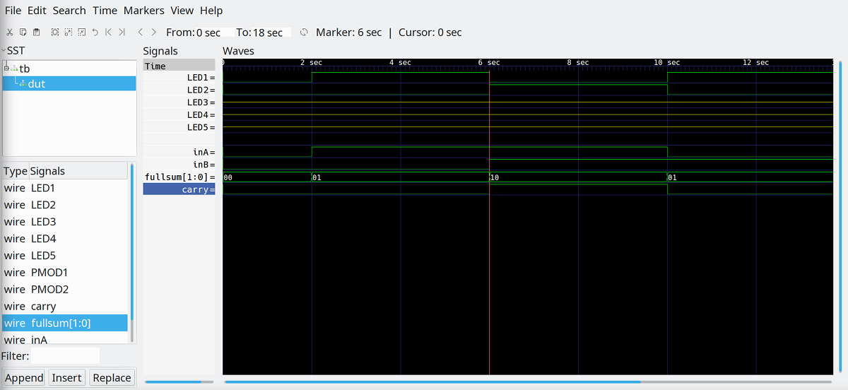
For now, you can focus on just the inA, inB, fullsum[1:0] and carry signals:
![]()
You can verify that the inputs all produce expected outputs. That's it! You've simulated an FPGA design using Verilog.
-
8▇▇▇▇ Get Ready for Bootcamp #2 ▇▇▇▇
![]()
In the second bootcamp, we'll look at sequential logic that uses clocks and flip flops. We will also do more with test benches and learn some more key points about Verilog. See you there!
-
9▇▇▇▇ Optional: Use an Offline Simulator ▇▇▇▇
If you don't want to use EDAPlayground you can download Icarus Verilog or install it from a software repository.
If you want to use it, you'll first want to save the files in the file section (design.v and testbench.v) to your working directory. Then you can use commands like this (the $ is the shell prompt):
$ iverilog -o demo testbench.v design.v
$ vvp demo
VCD info: dumpfile dump.vcd opened for output.
$ gtkwave dump.vcd
The gtkwave program lets you view the output of the simulation. You can install it from the web or your package manager.
![]()
The iverilog command compiles your Verilog into an executable program that does the actual simulation. The vvp command runs that executable. You can often just execute the program directly, but vvp offers you extended options like setting search paths and log files.
You can actually write things directly to the screen with $display, if you like. For example, try this testbench (you can download it as testbench-display.v in the files section):
`default_nettype none

// Simple test bench for iCEStick demo

module tb;
// simulus: a and b
reg a, b;
// results: 5 leds
wire led1, led2, led3, led4, led5;
// create Device Under Test and wire it up
demo dut(led1,led2,led3,led4,led5,a,b);

  initial   begin           // save data for later      $dumpfile("dump.vcd");
$dumpvars(0, dut);
$display("Start");
a=1'b0;
b=1'b0;
$display(a);
$display(b);
#2
a=1'b1;
$display(a);
$display(b);

#4
b=1'b1;
$display(a);
$display(b);
#4
a=1'b0;
$display(a);
$display(b);
#4

b=1'b0;
$display(a);
$display(b);
#4      $finish;
end
Notice the only change is the addition of $display statements. Keep in mind, things like $display are only for the testbench. They won't work at all on the FPGA.
 Al Williams



Discussions
Become a Hackaday.io Member
Create an account to leave a comment. Already have an account? Log In.
When I run this in EDAPlayground on my ChromebookI get "design.sv: 44: syntax error, I give up, Exit code expected: 0, received: 1...but, there is no line 44 in design.sv.
Running on my Windows 7 system, all runs fine.
Are you sure? yes | no