-
Developing Firmware for the OOD11
06/27/2018 at 22:08 • 0 comments -
OOD Meets STUPID
06/22/2018 at 19:21 • 0 comments -
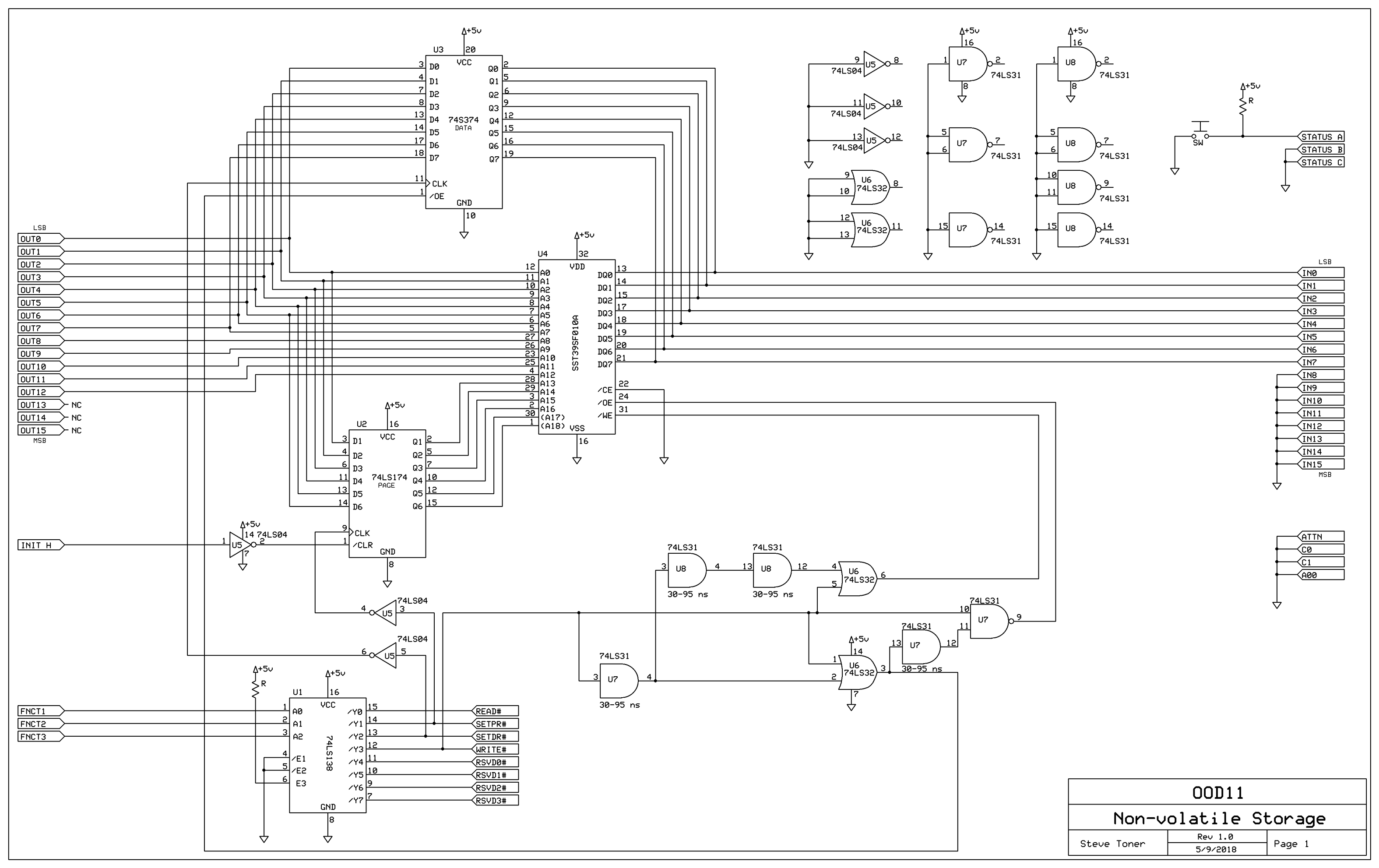
Non Volatile Storage
05/21/2018 at 02:23 • 0 commentsImplementing something roughly equivalent to floppy disk storage in terms of size & speed...
Schematic of custom board that interfaces to the DRV11-WA adapter:
![]() Although the schematic shows most parts as 74LS devices, I used what I had (except for the 74LS31s, which I had to order), so U1, U3, U5 & U6 are 74S parts while U2 is a 74F...
Although the schematic shows most parts as 74LS devices, I used what I had (except for the 74LS31s, which I had to order), so U1, U3, U5 & U6 are 74S parts while U2 is a 74F... -
Screwing Up So You Don't Have To
05/06/2018 at 16:59 • 0 commentsOK, the RUN light is now working. Those DEC engineers are perhaps a bit more clever than I gave them credit for. The AF1 signal on the bus is, well it's not bussed together across card slots. Slot 1 connects this line to the front panel connector, which drives the RUN light, which means that the processor needs to go in slot 1 if you want the run light to work.
But that wasn't the problem.
On my board, the SRUN L signal from the front panel connector drives a 7407 open collector gate, which drives the LED. I, uh... forgot/neglected/failed to connect the lead from the front panel connector to the input of the 7407 on my board. Having now wired it, the RUN light comes on at the appropriate time.
So what's the deal with it measuring 3.5VDC? Well, I suppose I should have looked at it with an oscilloscope rather than a DC voltmeter. It's not constantly on (pulled to ground), so I expect that it was acting rather like a PWM signal to the voltmeter...
-
Introducing the OOD11
05/06/2018 at 02:16 • 0 commentsWhile reviewing this video before posting, I noticed two things:
- The jumper on the MXV11 board that I said enables the RAM is in the wrong place! Apparently I held the board upside down (bus fingers pointing north instead of south) when trying to identify the location of W5. So why did it work? I have no idea what this location is for (looked at photos of other MXV11 boards, and none have a jumper in this location), but it isn't W5 so the RAM should have been disabled and my test should have failed. I moved the jumper and everything still works, so apparently no damage done.
- The RUN light didn't come on. This is driven by E54 on the CPU board, a 74LS138. It should be pulling it low, but it only goes to 3.5V. Thinking the chip could be bad, I replaced it, but no change. Then I started poking around with my multimeter. Turns out the MXV11 board connects the "open collector output of the clock" to bus line AF1, which is identified as SRUN L/SSpare 2. So presumably it has a pullup to +5V, and that's too strong for the 74LS138 to overcome. But why, DEC, WHY??? I can only presume that the MXV11 board predates the definition of AF1 as SRUN L, so this board is not fully compatible with the CPU board as is. You enable the clock on the MXV11 by jumpering J3 (which connects to AF1/clock out) and J4 (which connects to BEVENT L: BR1 on the bus). So there is no need for the MXV11 to be connecting to AF1 on the bus, and I will try cutting the trace. Seems like this should have been documented in a micronote somewhere, but I haven't seen it...
[Update: it is NOT necessary to cut the trace. See next log entry.]
-
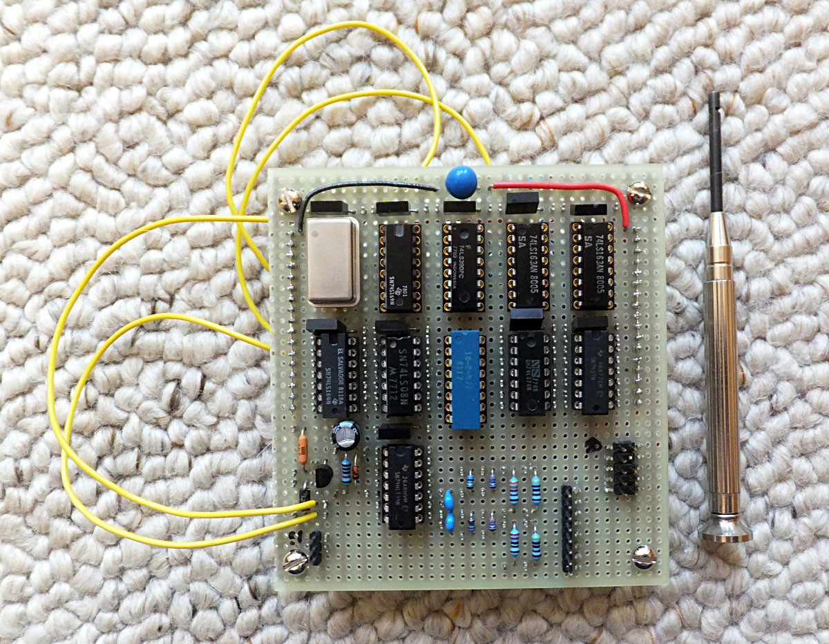
Control & Timing Board
04/28/2018 at 21:41 • 0 commentsOK, while I'm waiting on parts to get the M8047 working, let's go back and look at the control & timing board. Again, the goal here was to use parts I had on hand and that rule applied to the PCB and sockets as well as the chips. I had a cut-off piece of a prototyping board, about 4"x4". It has 2 holes-per-pad. I also had a few (35 year) old wire wrap sockets, so wire wrap seemed like the way to implement this board. I didn't have enough wire wrap sockets for all the parts, but I did have a whole bunch of wire wrap pins that can be soldered into the second hole next to a regular socket's pin and provide a means to wrap to that pin on the IC.
![]()
OK, so with parts from AVX, Bourns, ECS, Fairchild, Motorola, National Semiconductor, Signetics, Texas Instruments and I-don't-know-who-all, here is the board:
![]()
The top row has the nice gold-plated wire wrap sockets, and the rest of the sockets are of the solder tail variety, as you can see. The tool on the right is a manual wire wrapping (and unwrapping!) tool, also on the order of 35-40 years old. I think I got it at Radio Shack back in the day... Also, note the power and ground buses on the upper half of the right & left sides of the board. That blue "chip" in the middle is actually 15 resistors (pin 16 is common), which are used as pullups.
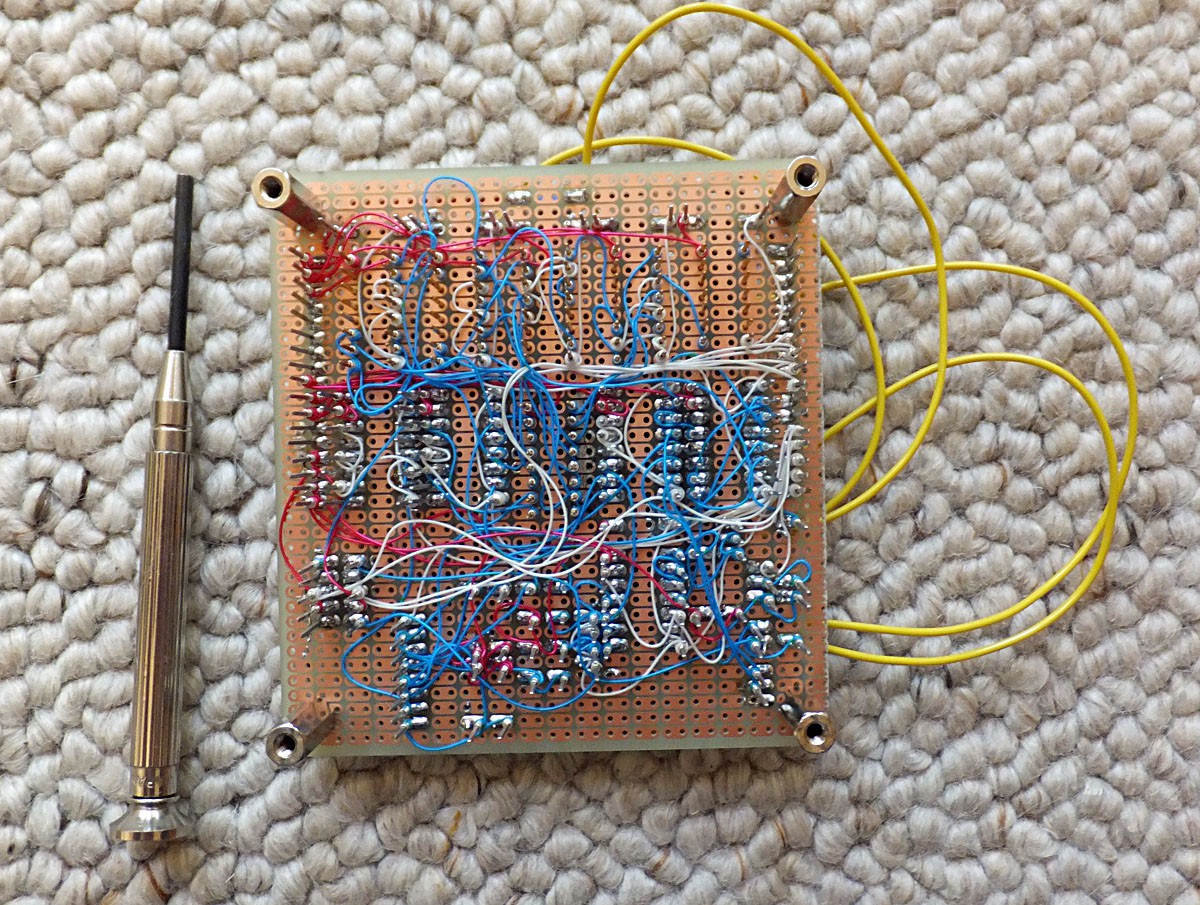
The bottom side of the board:
![]()
I had some old red & white wire, so used red for +5V and white for GND. The blue wire is of more recent vintage.
-
Status Report
04/28/2018 at 02:05 • 0 commentsOK, some progress to report:
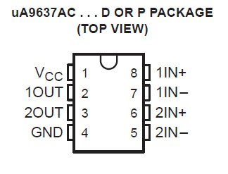
I reconfigured the M8047 back to default settings (except for baud rates). Set SLU1 to 300 baud and connected to a Silent 700 terminal. Powered on and...nothing. Turns out the 1A fuse on the +12V line on the M8047 was blown. I don't have any proper replacements right now (Littlefuse PICO II is a good replacement), so I ordered some and temporarily replaced the blown fuse with a jumper. Now I get console ODT output when I power it on (yay! That means the power-on sequencing circuit is working!) but it will not accept input from the keyboard. This could be a cabling issue, or possibly a blown UA9637 receiver (or ...). All I know at this point is that the RRI pin on the UART is stuck at logic 1.
More to come...
...and as promised:
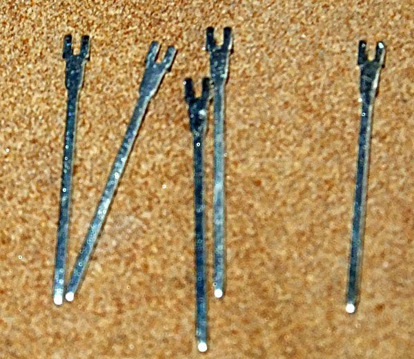
It does appear that the UA9637 is fried. I can trace the TTY output on the oscilloscope to pin 5 (2 IN-), but there is no change on pin 3 (2 OUT).
![]()
Guess I need to make *another* Mouser order...
-
Timing Board Schematics
04/26/2018 at 02:54 • 0 commentsTo generate the power sequence timing signals, some sort of clock is required. Since I've limited myself to parts-on-hand, I'll use a 1 MHz oscillator. Now, I can't get a very accurate 60Hz signal out of that for the Line Time Clock (LTC), but I can get kind of close. I could run the LTC at 50Hz but I'm going with 60... I could let the M8047 generate the LTC signal, but if I need to replace it somewhere down the line for 22-bit address support, then I'll need another LTC source. So I might as well generate it on my board.
Approximating 60Hz
1 MHz is 60Hz * 16666.666... Like I said, I can't generate that exactly. But how about dividing by 16667? That would be within 20ppm. However, we want the result to have a 50% duty cycle and that will be hard when dividing by an odd number. So how about 16666? That's within 40ppm. But I don't have the chips to do it. If I had four 74LS163 (4-bit presettable) counters I could do it, but I only have two. Other chips I have on hand are a 74S169 (4-bit presettable up/down counter) and a 74LS390 (dual 4-bit decade counter). Using those, I can divide by 16660, and that'll generate 60.024Hz which is off by about 400ppm. Not good enough for a time-of-day clock. Oh well, close enough for my purposes.
Generating the Delays
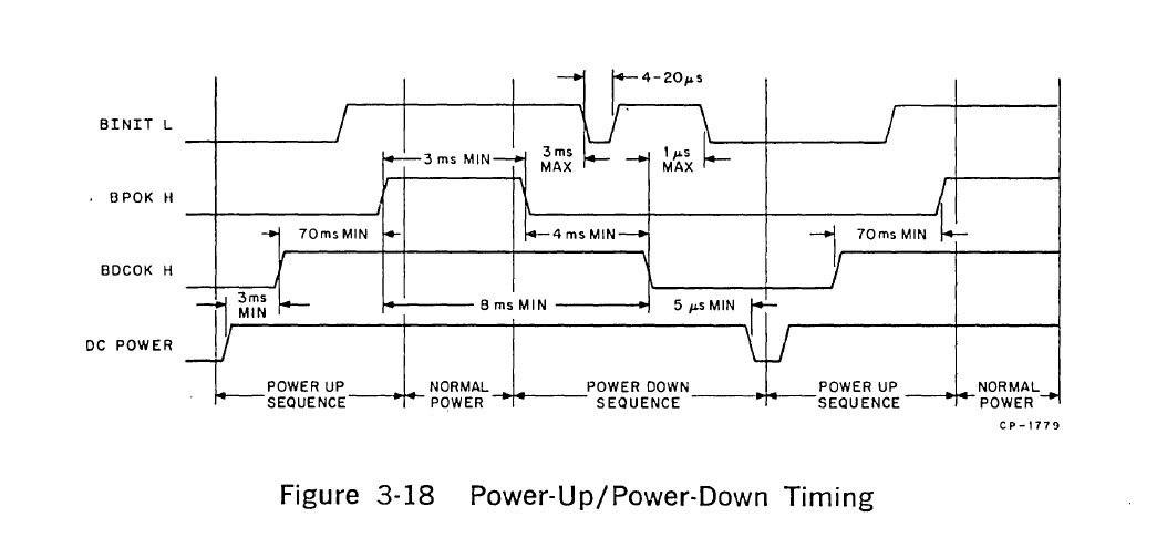
OK, so let's look at the timing diagram again:
![]()
After the +5V supply stabilizes, we have to wait at least 3msec before asserting BDCOK. Then we have to wait at least 70msec before asserting BPOK. A shift register clocked off our 60Hz signal can provide these delays.
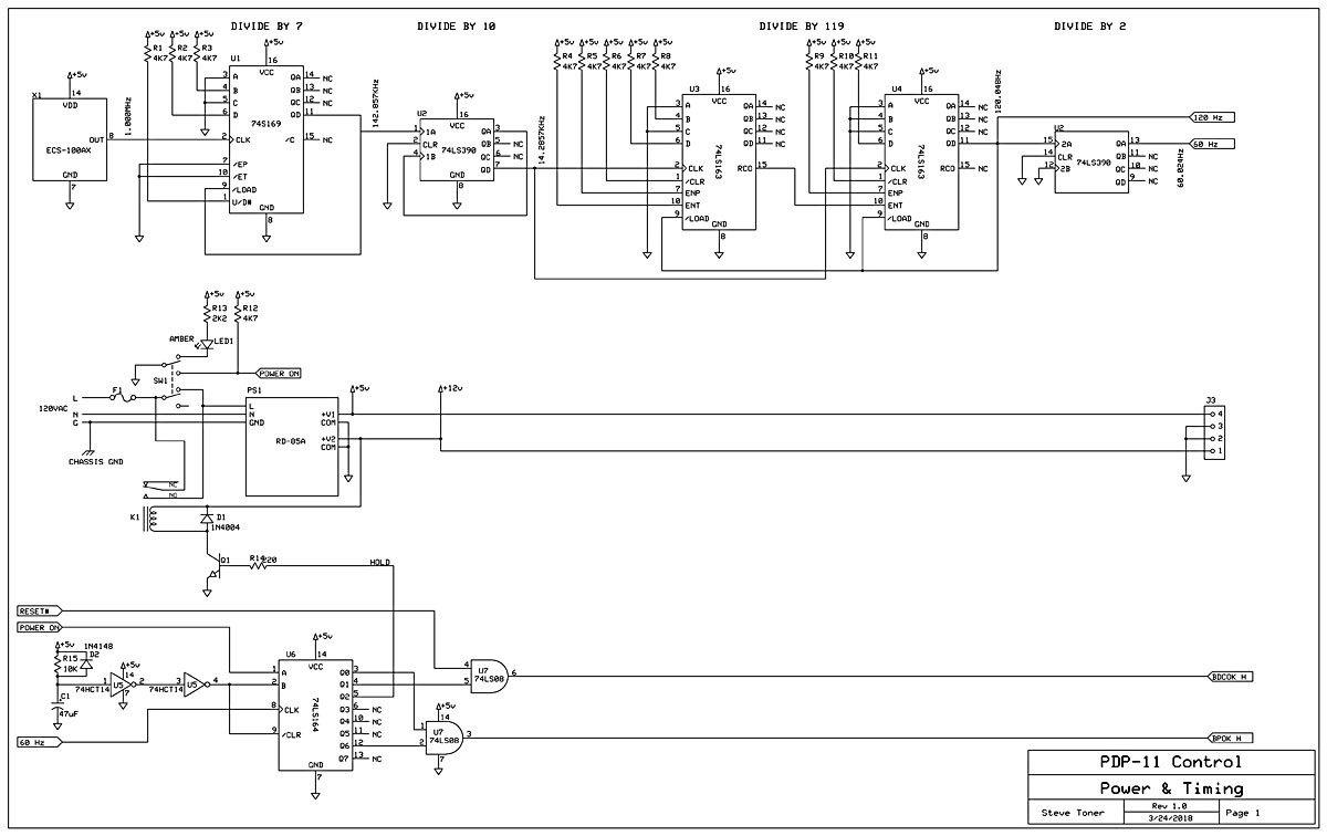
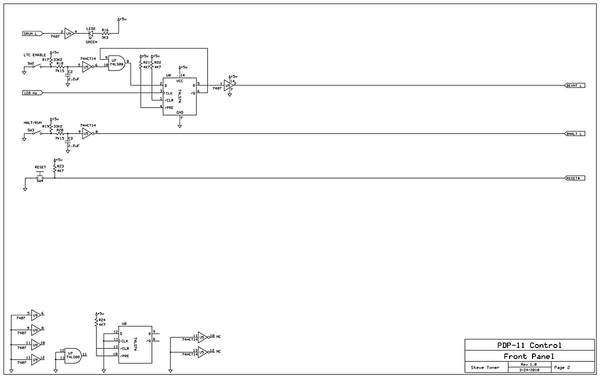
Schematics
![]()
![]()
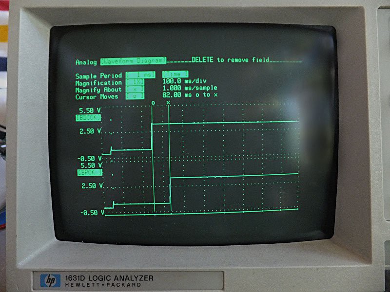
Verifying the Timing
Using the oscilloscope of the HP 1631D Logic Analyzer, we can view the signal timing:
![]()
The scope is triggering on the +5V power supply when it reaches 4.5V. The x and o markers show approximately 82 msec between BDCOK and BPOK, which is more than the required 70 msec. From +5V supply at 4.5V to BDCOK is around 250msec, which is well over the required 3 msec, even if we allow some time for the supply voltage to stabilize at 5.0V.
Building a PDP-11
Putting together a minimal LSI-11/23 from boards & parts
 Although the schematic shows most parts as 74LS devices, I used what I had (except for the 74LS31s, which I had to order), so U1, U3, U5 & U6 are 74S parts while U2 is a 74F...