agp.cooper
-
Almost Working
03/04/2019 at 23:24 • 0 commentsAlmost Working
Updated and tested the Software Data Protection version on the FRAM programmer.
I had set my self a trap! "A14" is not set using SetAddr(), It has its own routine. But it is working now. I have uploaded the code.
Endless Loop
I also wrote a Control Card simulation so I could test the bus. Surprisingly the CPU is mostly working before going into an endless loop.
It fails when I try to change the ROM Page. It should wait until a jump before changing the Page but it changes the Page immediately.
It seems as if the LOAD signal (which signals the PC to jump on the next clock) is glitched.
Using the logic analyzer I did (once) get it to show glitches every write machine cycle.
How to fix?
Cross-talk on the CLR Signal
I am getting about 5 clock cycles on the CLR signal as the Reset triggers reset schmitt trigger. It does not appear to affect (but there is some evidence that it does!) the control circuit. It could be internal cross-talk (as the clock and reset circuity share the same chip) or external cross-talk because the components are close together.
I am thinking of adding a 47 pF capacitor to the input gate of the reset logic.
Next time I will use a 74HC14 rather than build my own Schmitt trigger.
---
The capacitors did not work.
Redesigned the clock and reset circuity.
Redesigned the load signal to avoid the glitch areas between the machine cycles.
Redesigned the boards and sent them off to be made.
Bugger no sooner than I sent the order off I found an error.
Oh well, I will sent the updated board tomorrow.
I am getting close to working!
AlanX
-
Debugging
02/01/2019 at 06:33 • 0 commentsDebugging
Need to get this project working.
One problem is that the Nano does not have enough pins.
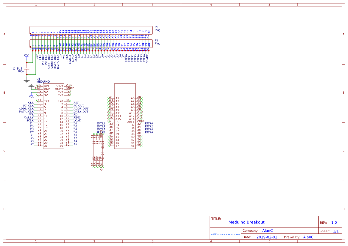
So I have used a Meduino (a Mega2560 Pro Mini).
Here is the schematic:
![]()
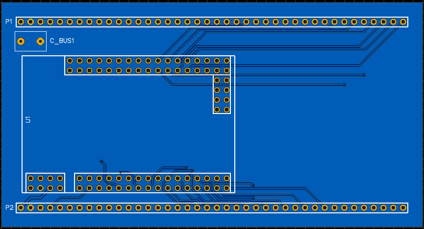
Here is the PCB:
![]()
The ports (P1 & P2) match the TTA8 bus.
A problem with the Meduino is that pins do not align with the ports (unlike the Nano).
So it is awkward to go fast. Awkward just means more coding. But do I really need to go fast? This time I have coded using pinMode, digitalRead and digitalWrite.
Here is the Mother Board I/O test code:
/*
  Front Panel Board Test
  ======================
REGISTERS:
  Hex  Address Write   Read      Comment
  FF   255     JMP     INTR      Jump/Intr
  FE   254     JC      Reserved  Jump on Carry
  FD   253     ROM     Reserved  ROM PAGE
  FC   252     RAM     Reserved  RAM PAGE
  FB   251     REGD    REGD      DATA REG
  FA   250     REGA    REGA      DATA REG ADDR
  F9   249     REGQ    NAND      ALU
  F8   248     REGP    ADD       ALU

SYSTEM (Pointer to Pointer Copy):
  Hex  Address Write   Read      Comment
  F7   247     JUMP    JUMP
  F6   246     POINTER POINTER
  F5   245     DEPOSIT DEPOSIT
  F4   244     FETCH   FETCH
  F3   243     DATA    DATA
  F2   242     ADDR    ADDR
  F1   241     RETURN  RETURN
  F0   240     PAGE    PAGE

CPU MODEL:
  Hex  Address Write   Read      Comment
  EF   239     TEMP    TEMP
  EE   238     DELAY   DELAY
  ED   237     INTR    INTR
  EC   236     MASK    MASK
  EB   235     PP      PP        Page Pointer
  EA   234     IP      IP        Instruction Pointer
  E9   233     SP      SP        Return Stack Pointer
  E8   232     DX      DX        (Monitor Data I/O)
  E7   231     CX      CX        (Monitor Addr I/O)
  E6   230     BX      BX
  E5   229     AX      AX
  E4   228     TX      TX        Temp Register
  E3   STACK
  E2   STACK
  E1   STACK
  E0   STACK
  ...

  0xF8-0xFF REGISTERS  (8 registers)
  0xC0-0xF7 STATIC RAM (56 bytes at page 0xFF)
  0x80-0xBF PAGED RAM  (64 bytes)
  0x00-0x7F PAGED ROM  (128 bytes)

  CPU Emulation:
    This CPU has no actual opcodes.
    All instructions are MOVE from [PC] to [PC+1]
    i.e. Move DATA from source ADDRess to destination ADDRess.

    The 4 cycles are:
    1 Fetch the destination ADDRess pointed to by the program counter and put in the ADDR register
    2 Fetch destination DATA pointed to by the ADDR register and put and the DATA register
    2A  Increment the program counter (PC)
    3 Fetch destination ADDRess pointed to by the program counter and put in the ADDR register
    4 Deposit the DATA register into the destination pointed to by the ADDR register
    4A  Increment the program counter (PC)

    All hardware (PC,IO and ALU) is memory mapped.
*/

// Board Connections:
//       Bus       Meduino Pin
//       VCC
//       GND       Gnd
#define  RST       2
#define  CLR       3
#define  PC_OUT    4
#define  PC_CLK    5
#define  ADDR_OUT  6
#define  ADDR_CLK  7
#define  DATA_OUT  8
#define  DATA_CLK  9
#define  RD        10
#define  WR        11
#define  REGS      12
#define  CARRY     13
#define  LOAD      14
#define  SCLK      15
#define  Data0     16
#define  Data1     17
#define  Data2     18
#define  Data3     19
#define  Data4     20
#define  Data5     21
#define  Data6     22
#define  Data7     23
#define  Addr0     24
#define  Addr1     25
#define  Addr2     26
#define  Addr3     27
#define  Addr4     28
#define  Addr5     29
#define  Addr6     30
#define  Addr7     31
#define  Intr0     32
#define  Intr1     33
#define  Intr2     34
#define  Intr3     35
#define  Intr4     36
#define  Intr5     37
#define  Intr6     38
#define  Spare     39

void InitialiseBoard(void)
{ // Reset State
  pinMode(RST,INPUT_PULLUP);   // Dont care
  pinMode(CLR,OUTPUT);         digitalWrite(CLR,LOW);
  pinMode(PC_OUT,OUTPUT);      digitalWrite(PC_OUT,LOW);
  pinMode(PC_CLK,OUTPUT);      digitalWrite(PC_CLK,LOW);
  pinMode(ADDR_OUT,OUTPUT);    digitalWrite(ADDR_OUT,HIGH);
  pinMode(ADDR_CLK,OUTPUT);    digitalWrite(ADDR_CLK,LOW);
  pinMode(DATA_OUT,OUTPUT);    digitalWrite(DATA_OUT,HIGH);
  pinMode(DATA_CLK,OUTPUT);    digitalWrite(DATA_CLK,LOW);
  pinMode(RD,OUTPUT);          digitalWrite(RD,HIGH);
  pinMode(WR,OUTPUT);          digitalWrite(WR,HIGH);
  pinMode(REGS,OUTPUT);        digitalWrite(REGS,HIGH);
  pinMode(CARRY,OUTPUT);       digitalWrite(CARRY,LOW);
  pinMode(LOAD,OUTPUT);        digitalWrite(LOAD,HIGH);
  pinMode(SCLK,OUTPUT);        digitalWrite(SCLK,HIGH);
  pinMode(Data0,INPUT_PULLUP);
  pinMode(Data1,INPUT_PULLUP);
  pinMode(Data2,INPUT_PULLUP);
  pinMode(Data3,INPUT_PULLUP);
  pinMode(Data4,INPUT_PULLUP);
  pinMode(Data5,INPUT_PULLUP);
  pinMode(Data6,INPUT_PULLUP);
  pinMode(Data7,INPUT_PULLUP);
  pinMode(Addr0,OUTPUT);       digitalWrite(Addr0,LOW);
  pinMode(Addr1,OUTPUT);       digitalWrite(Addr1,LOW);
  pinMode(Addr2,OUTPUT);       digitalWrite(Addr2,LOW);
  pinMode(Addr3,OUTPUT);       digitalWrite(Addr3,LOW);
  pinMode(Addr4,OUTPUT);       digitalWrite(Addr4,LOW);
  pinMode(Addr5,OUTPUT);       digitalWrite(Addr5,LOW);
  pinMode(Addr6,OUTPUT);       digitalWrite(Addr6,LOW);
  pinMode(Addr7,OUTPUT);       digitalWrite(Addr7,LOW);
  pinMode(Intr0,INPUT_PULLUP);
  pinMode(Intr1,INPUT_PULLUP);
  pinMode(Intr2,INPUT_PULLUP);
  pinMode(Intr3,INPUT_PULLUP);
  pinMode(Intr4,INPUT_PULLUP);
  pinMode(Intr5,INPUT_PULLUP);
  pinMode(Intr6,INPUT_PULLUP);
  pinMode(Spare,INPUT_PULLUP);
}

bool Reset(void)
{
  byte data;

  data=digitalRead(RST);
  if (data==0) {
    digitalWrite(CLR,LOW);
    return true;
  } else {
    digitalWrite(CLR,HIGH);
    return false;
  }
}

byte ReadAddr(byte addr)
{
  byte data;

  // SET DATABUS TO INPUT
  pinMode(Data0,INPUT_PULLUP);
  pinMode(Data1,INPUT_PULLUP);
  pinMode(Data2,INPUT_PULLUP);
  pinMode(Data3,INPUT_PULLUP);
  pinMode(Data4,INPUT_PULLUP);
  pinMode(Data5,INPUT_PULLUP);
  pinMode(Data6,INPUT_PULLUP);
  pinMode(Data7,INPUT_PULLUP);

  // SELECT ADDRESS
  digitalWrite(Addr0,addr&1);
  digitalWrite(Addr1,(addr>>1)&1);
  digitalWrite(Addr2,(addr>>2)&1);
  digitalWrite(Addr3,(addr>>3)&1);
  digitalWrite(Addr4,(addr>>4)&1);
  digitalWrite(Addr5,(addr>>5)&1);
  digitalWrite(Addr6,(addr>>6)&1);
  digitalWrite(Addr7,(addr>>7)&1);

  // READ DATA
  if (addr>=248) digitalWrite(REGS,LOW);
  digitalWrite(RD,LOW);
  delayMicroseconds(10);
  data=digitalRead(Data0);
  data|=digitalRead(Data1)<<1;
  data|=digitalRead(Data2)<<2;
  data|=digitalRead(Data3)<<3;
  data|=digitalRead(Data4)<<4;
  data|=digitalRead(Data5)<<5;
  data|=digitalRead(Data6)<<6;
  data|=digitalRead(Data7)<<7;
  digitalWrite(RD,HIGH);
  if (addr>=248) digitalWrite(REGS,HIGH);
  return(data);
}

void WriteAddr(byte addr,byte data)
{
  // SELECT ADDRESS
  digitalWrite(Addr0,addr&1);
  digitalWrite(Addr1,(addr>>1)&1);
  digitalWrite(Addr2,(addr>>2)&1);
  digitalWrite(Addr3,(addr>>3)&1);
  digitalWrite(Addr4,(addr>>4)&1);
  digitalWrite(Addr5,(addr>>5)&1);
  digitalWrite(Addr6,(addr>>6)&1);
  digitalWrite(Addr7,(addr>>7)&1);

  // WRITE DATA
  if (addr>=248) digitalWrite(REGS,LOW);
  pinMode(Data0,OUTPUT);
  pinMode(Data1,OUTPUT);
  pinMode(Data2,OUTPUT);
  pinMode(Data3,OUTPUT);
  pinMode(Data4,OUTPUT);
  pinMode(Data5,OUTPUT);
  pinMode(Data6,OUTPUT);
  pinMode(Data7,OUTPUT);
  digitalWrite(Data0,data&1);
  digitalWrite(Data1,(data>>1)&1);
  digitalWrite(Data2,(data>>2)&1);
  digitalWrite(Data3,(data>>3)&1);
  digitalWrite(Data4,(data>>4)&1);
  digitalWrite(Data5,(data>>5)&1);
  digitalWrite(Data6,(data>>6)&1);
  digitalWrite(Data7,(data>>7)&1);
  digitalWrite(WR,LOW);
  delayMicroseconds(10);
  digitalWrite(WR,HIGH);
  if (addr>=248) digitalWrite(REGS,HIGH);

  // RESET DATABUS
  pinMode(Data0,INPUT_PULLUP);
  pinMode(Data1,INPUT_PULLUP);
  pinMode(Data2,INPUT_PULLUP);
  pinMode(Data3,INPUT_PULLUP);
  pinMode(Data4,INPUT_PULLUP);
  pinMode(Data5,INPUT_PULLUP);
  pinMode(Data6,INPUT_PULLUP);
  pinMode(Data7,INPUT_PULLUP);
}

void setup() {
  // Fire up the board
  InitialiseBoard();

  // Serial.begin(9600);
  // while (!Serial);
  // Serial.println();
}

void loop() {
  byte A=0;

  // Check reset button
  if (!Reset()) {
    // ADDR LEDs and Switches
    WriteAddr(0XFA,0X00);
    A=ReadAddr(0XFB);
    WriteAddr(0XFB,A);
    // DATA LEDs and Switches
    WriteAddr(0XFA,0X01);
    A=ReadAddr(0XFB);
    WriteAddr(0XFB,A);
  } else {
    // RESET State
    // ADDR LEDs
    WriteAddr(0XFA,0X00);
    WriteAddr(0XFB,0xFF);
    // DATA LEDs
    WriteAddr(0XFA,0X01);
    WriteAddr(0XFB,0xFF);
  }
  delay(100);
}
Testing
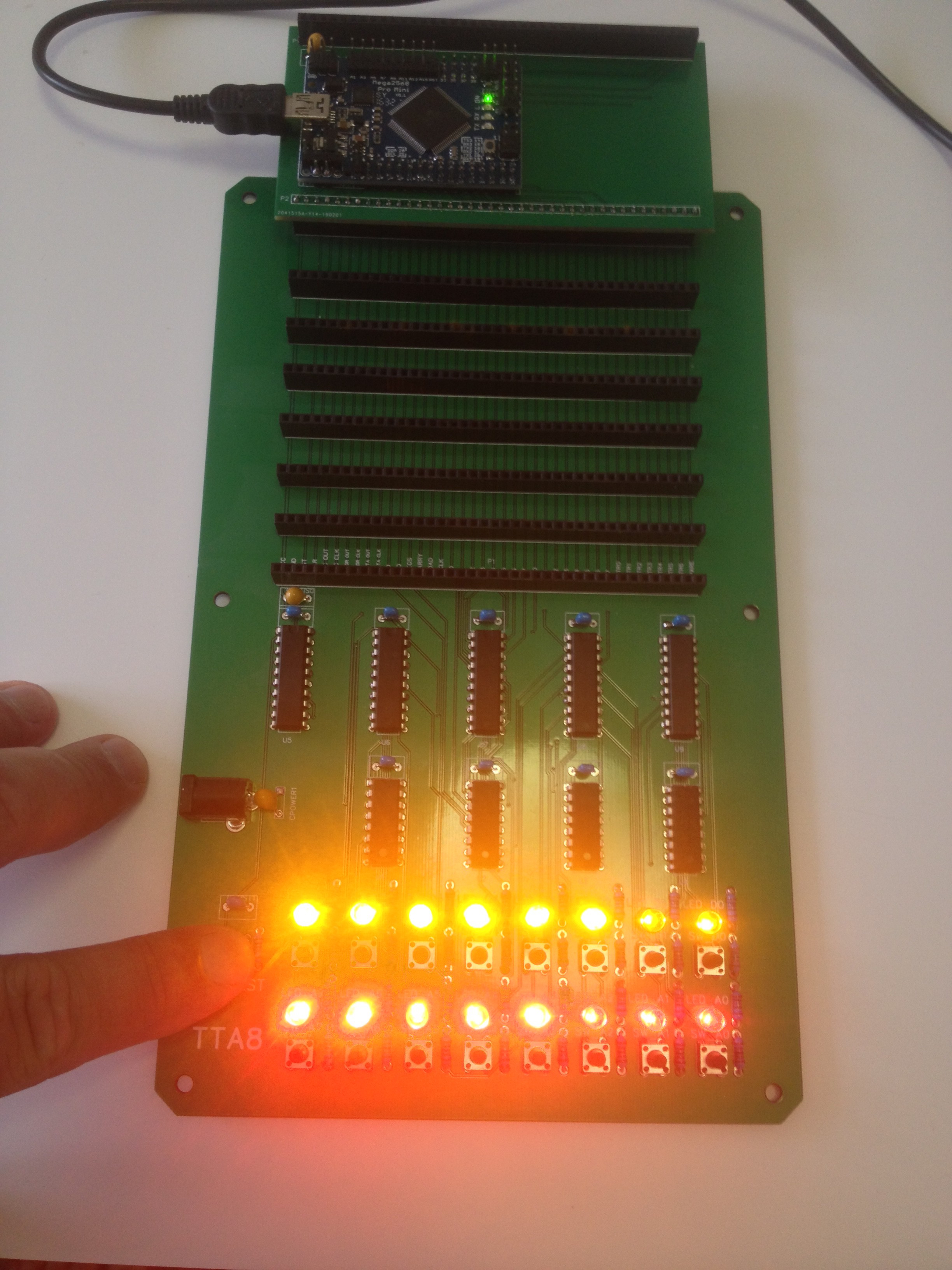
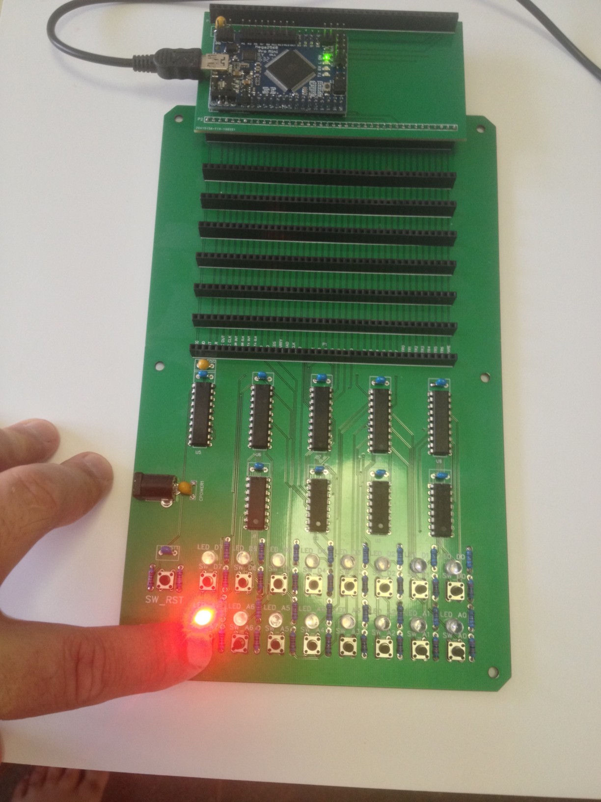
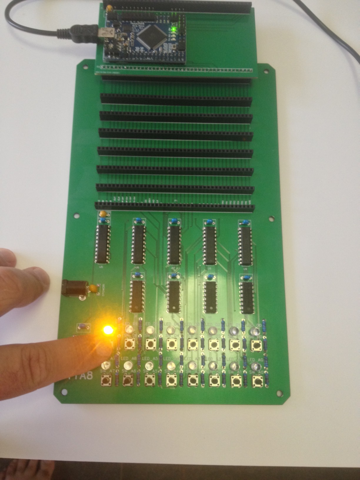
Fired up first time! Wow! Okay, I know the Mother Board works.
Here is the reset:
![]()
Here is A7:
![]()
And D7:
![]()
Trust me the rest work.
ALU Board
Next is the ALU Board. It works, no surprise as it tested out before.
ROM/RAM/StaticRAM Board
No it does not work. So far I have found two errors. The ROM page and RAM page are swapped, and the Static RAM (Addresses 192 to 247) are latched (wrong).
I forgot that the ROM/RAM pages are latched by a jump (i.e. JC or JMP).
For testing purposes I can fix these in software but still I cannot read the ROM or RAM data. I have to rework the code to make it easier to log the bus (i.e with a bus analyser).
Still no life out of the board. So the it is a chip select problem. Yes, U4 expects REGS high but I design REGS low.
Fix. I can't fix this in software so time for a new board.
Interrupt Board
This board generates SCLK which is 38400 Hz. It uses the WR signal from the Controller Board. There is always a WR (and a RD) every 8 clock cycles (no more and no less).
Interrupts Intr0 through to Intr6 are external while Intr7 is connected to a 2400 Hz clock (SCLK/16). The interrupt address is 0xFF (read only). Reading the interrupt address clears Intr7. Intr& is used to control the serial card (along with SCLK).
Anyway, my tests tell me the Interrupt/Timing Board is working.
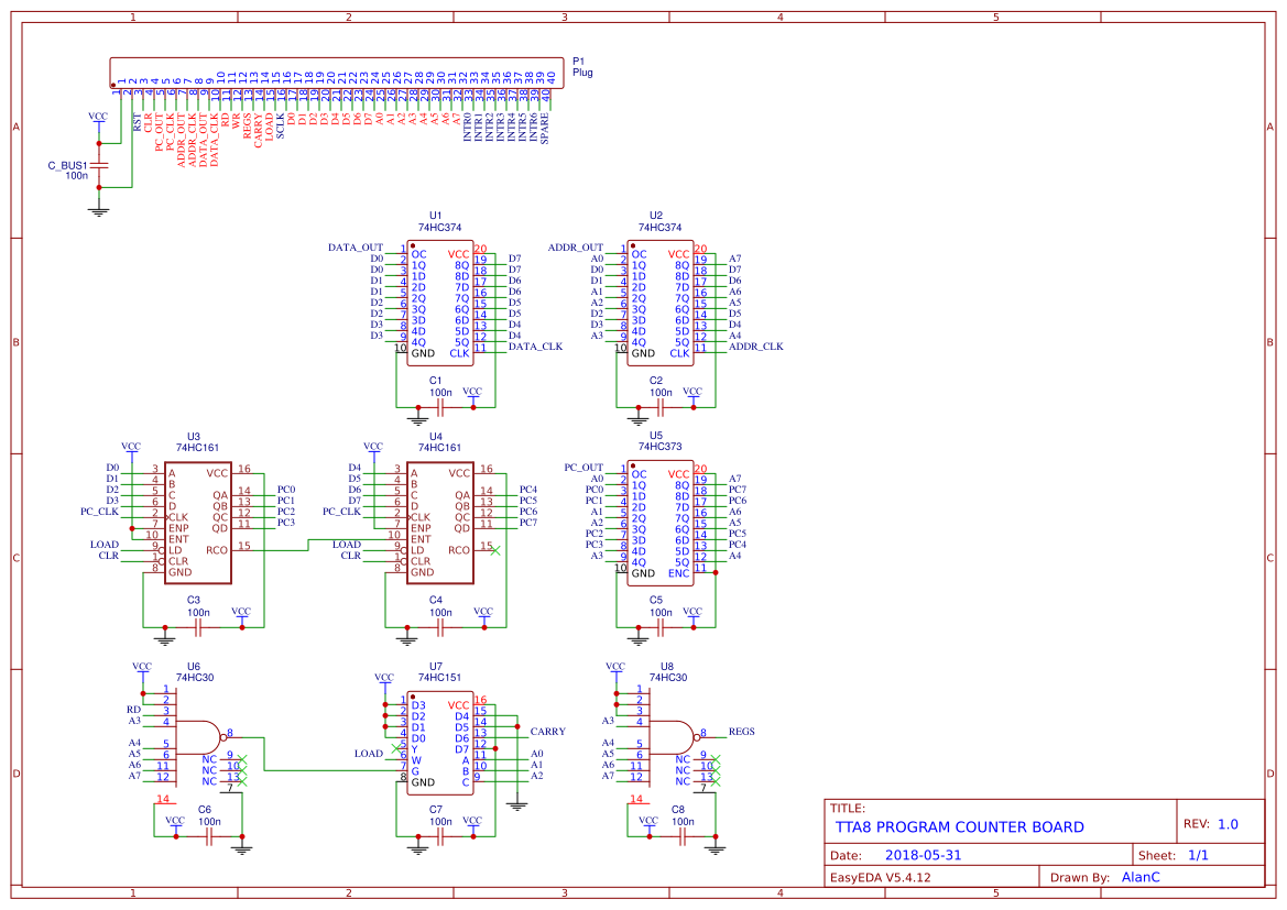
Program Counter Board
This board is controlled by the Controller Board (which previously tested okay (at least by the logic analyzer)).
Other than the Serial Board, this is the last board to test.
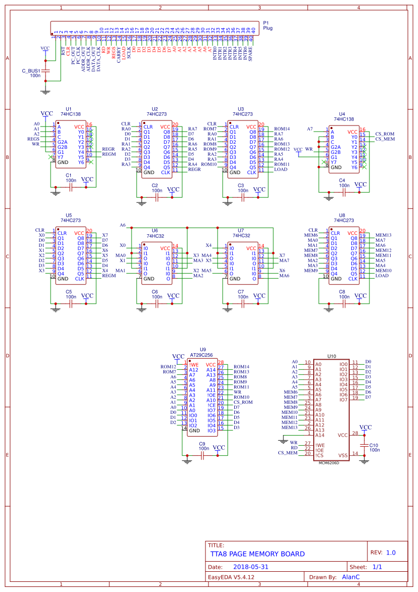
New Paged Memory Board
Populated the new Paged Memory Board.
Plug in Mother Board - Fail.
Test the Paged Memory Card:
- Tested Paged RAM - check.
- Tested Static RAM - check.
- Tested Paged ROM:
- Page 0 - Corrupted.
- Pages 1+ - Okay.
Check FRAM in programmer:
- Check - Page 0 correupted.
- Reprogram FRAM
Recheck Paged Memory Card:
- Check - All good.
Plug in Mother Board - Fail.
Test the Paged Memory Card:
- Page 0 - Corrupted.
- Otherwise all good.
This means something is writing to the FRAM as the WR signal is exposed.
Could be code or hardware responsible.
Something to look at tomorrow, otherwise progress has been made.
---I set Software Data Protection (SDP) mode on the AT29C256 FRAM.
At least I think I have? I will find out shortly.
Anyway should not have to reprogram the FRAM after each test.
Now to find out why, is it the Monitor code or a hardware problem?
AlanX
-
Assembled Paged Memory and Interrupt Boards
08/17/2018 at 06:41 • 0 commentsAssembled the Last Two Boards
I will skip the board testing and will code the Monitor to the FlashROM (AT29C256).
You never know I may get lucky.
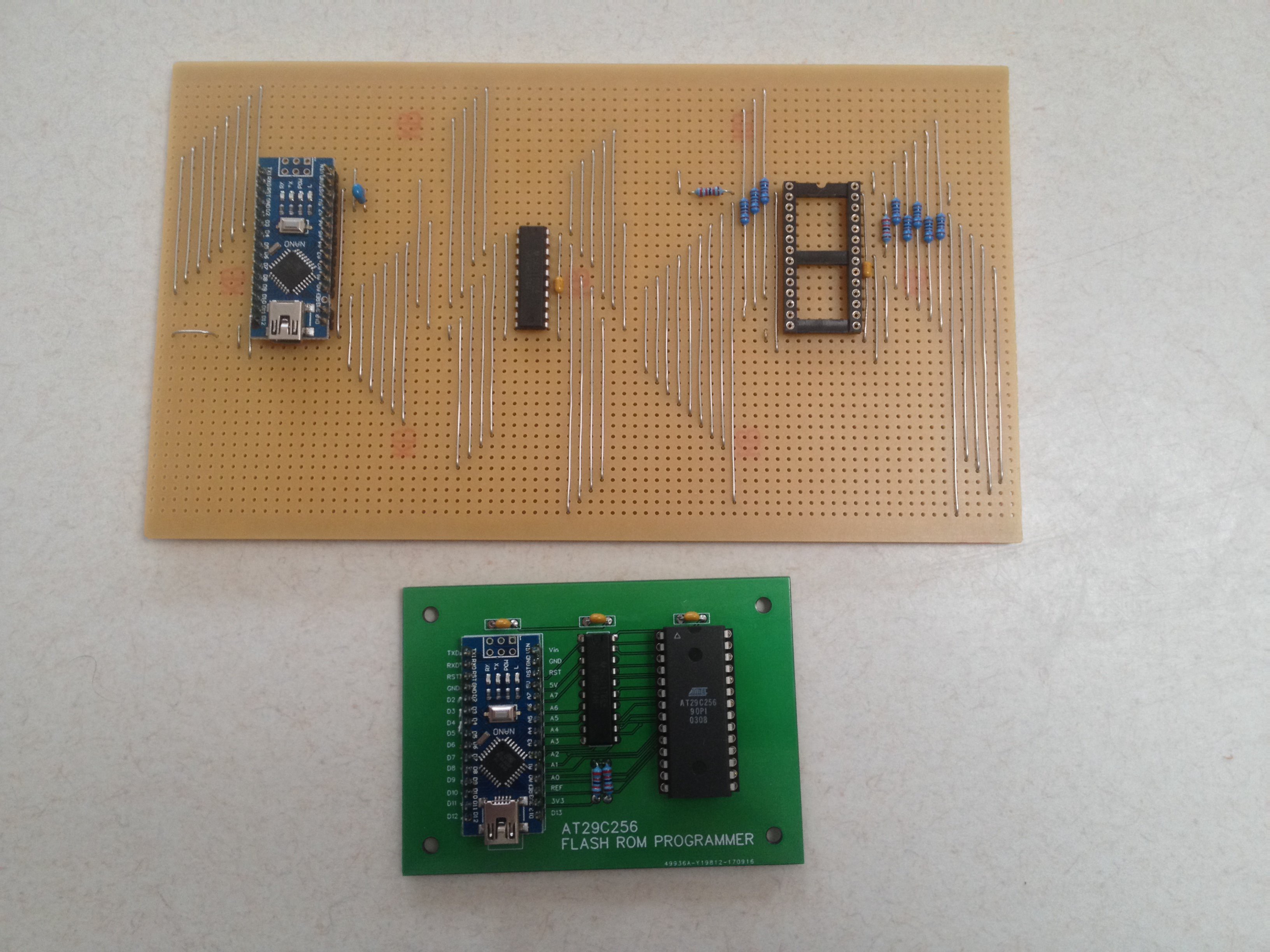
I designed and build a Nano controlled FlashROM programmer a while back:
![]()
Programmer Failure?
I loaded the AT29C256 chip into the stripboard version of my Flash ROM programmer, uploaded my code but it did not work (i.e. load). Stripboard sometimes needs to be cleaned if it has been sitting around for a while. Still no. Found the PCB version of the programmer and still no? Salvaged a known good chip and the programmer was fine. Another bad AT29C256 chip! I have had a few bad chips so I was sort of expecting it.
Loaded the chip into the Page Memory board and no. So I need to test the board.
AlanX
-
Mother Board Tested
07/27/2018 at 08:36 • 0 commentsMother Board Tested
Okay, finally got around to assembling and testing the lastest Mother Board.
All good. Uploaded the Arduino sketch (TTA8_IO_TestWorking.ino) that I used.
---
I have been busy following the Australian "My Healt Record" debacle. It is just amazing how bad politicians lie and how little regard they have for the public.
---
I have more boards that need to be assembled and tested.
ALU Board Tested
You can add the ALU board to the pass list.
The Timing Board passed the logic analyser test previously.
I have double checked the Program Counter Board but it's hard to test so it passed for the moment.
I will assemble the Timer/Interrupt Board next.
Ordered some 74HC273 chips. Should arrive by friday. After that I can assemble and test the Paged ROM/RAM Memory Board. The ROM code is ready, just need to set up the programmer.
I have assembled a Serial I/O Board but testing can wait.
AlanX
-
Another Bad Board
07/05/2018 at 09:10 • 0 commentsAnother Bad Board
I assembled the new Mother Board, hooked up the Nano and no, it did not work.
I had swapped RD and WR signals but still the Data LEDs did not light. Checked the code (worked as expected last time), the hookup and then the schematic. All good, the Nano reports that the Data switches work so it had to be the PCB. Yes, I must have forgotten to update PCB after the last schematic update. The LED Data WR signal is a mess. Its not just a simple jumper.
Oh well, I may as well check all the other boards and get all the corrected PCBs at one time.
Need to do some research on Forth internals as well.
The PC board has a fault as well. Using jumpers for everything means you have to check the jumper labels very carefully.
And more bad boards. Made corrections and sent off for remanufacture.
AlanX
-
More Code
07/04/2018 at 12:33 • 0 commentsAnother Day and More Code Written and Tested
I now have five Interpreter Instructions:
- Inline (for natice micro-code)
- JMP
- JZ (AX==0)
- Call
- RTN
Most the time was spent squeezing the code into a Page.
The code is roughly twice as long as the orginal code written for the unpaged TTA8 (i.e. Weird CPU). But much more difficult to write and test (i.e. more traps to avoid)!
More code to write:
- Push
- Pop
- Load Immediate
- Multiply
- Divide
- etc.
But it would be better to get the hardware going.
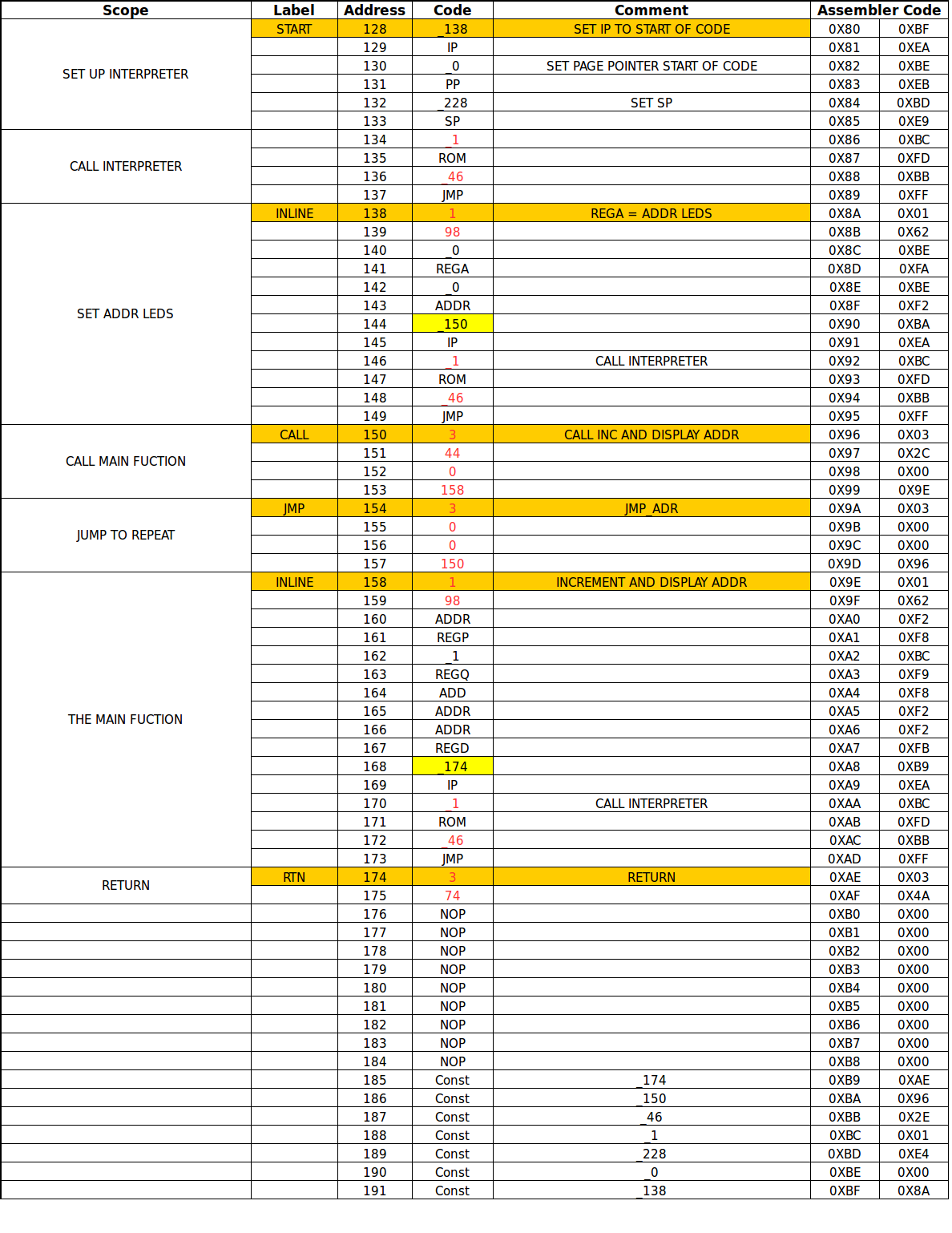
Just for the record, here is the counter code:
![]()
The current Emlator Version is 9.
AlanX
-
Paged TTA8 Interpreter Conclusion
07/02/2018 at 05:07 • 0 commentsInterpreter Conclusion
The Interpreter is written (and tested) so it is done.
But it is not the end of the Paged TTA8.
This version is much more code expensive than anticipated but still workable.
A non-paged 16 bit version would be much better.
There is still work to complete and test the hardware version.
And to add Interrupts and Serial Communications.
And finally an operating system, perhaps based on Forth.
Added the Interrupt Service Routine
I added support for Interrupts. Each time the Interpeter is called it first checks for an interrupt. Most microcomputers have an address lookup area for storing interrupt service rountine addresses (i.e. it allows software customisation). In my case I just reserved ROM page 3 for ISRs. I will come back to it later (for the serial card).
I also used a timeout on the emulator switches rather than a two clicks (i.e. one on and one off), just a nicety.
I think I have done enough to put together the hardware version of the Paged TTA8.
AlanX
-
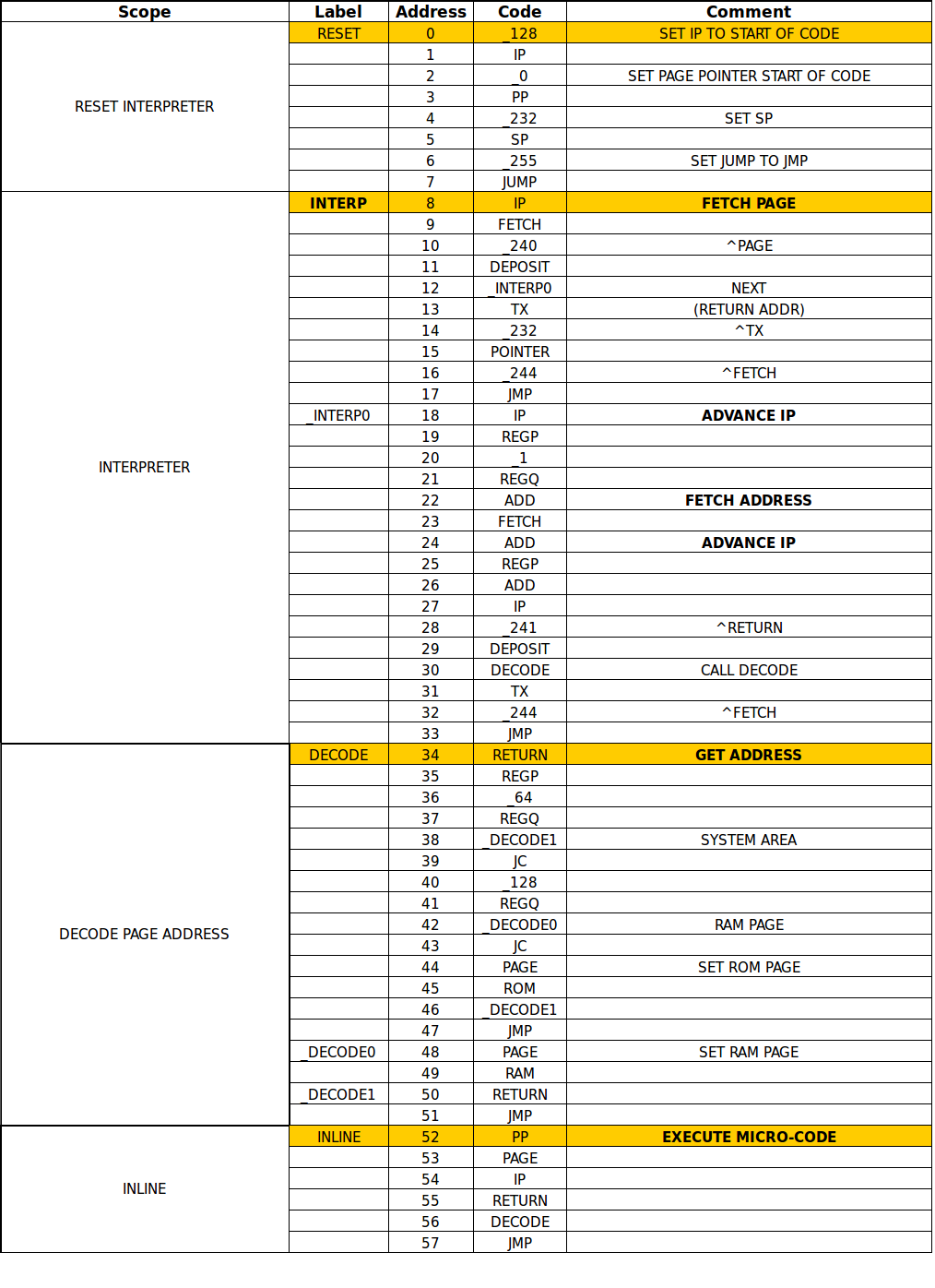
Interpreter Up and Running
07/02/2018 at 05:00 • 0 commentsInterpret Up and Running
Some social duties have intervened on my TTA8 work. Today was the first opportunity to spend time on the project.
The Interpreter is now working but it is much bigger (slower) than expected.
Here is the simple version:
INTERP		IP	SAVE IP
		POINTER
		IP	INC IC
		REGP
		_1
		REGQ
		ADD
		IP
		_246	^POINTER
		JMP
Here is the Paged version:
INTERP	8	IP	FETCH PAGE
	9	FETCH
	10	_240	^PAGE
	11	DEPOSIT
	12	_INT0	NEXT
	13	TX	(RETURN ADDR)
	14	_232	^TX
	15	POINTER
	16	_244	^FETCH
	17	JMP
_INT0	18	IP	ADVANCE IP
	19	REGP
	20	_1
	21	REGQ
	22	ADD	FETCH ADDRESS
	23	FETCH
	24	ADD	ADVANCE IP
	25	REGP
	26	ADD
	27	IP
	28	_241	^RETURN
	29	DEPOSIT
	30	_INT1	NEXT
	31	TX
	32	_244	^FETCH
	33	JMP
_INT1	34	DECODE	CALL DECODE
	35	JMP
Note the Paged Interpreter also calls Decode.
The Counter Program
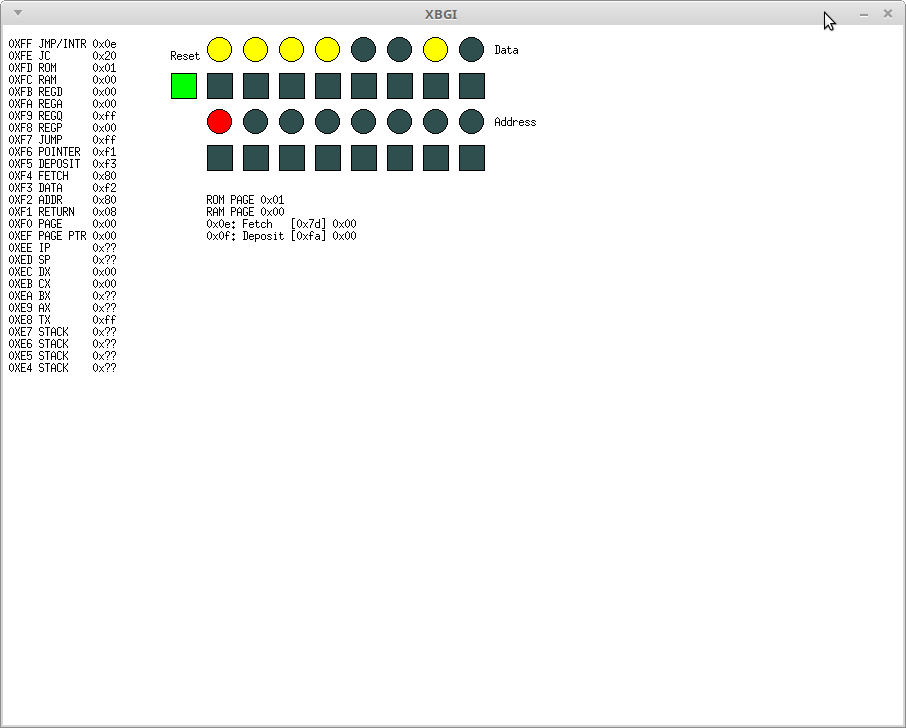
The counter progrm first sets up the Interpreter and only uses Inline (to revert bck to Machine Code):
![]()
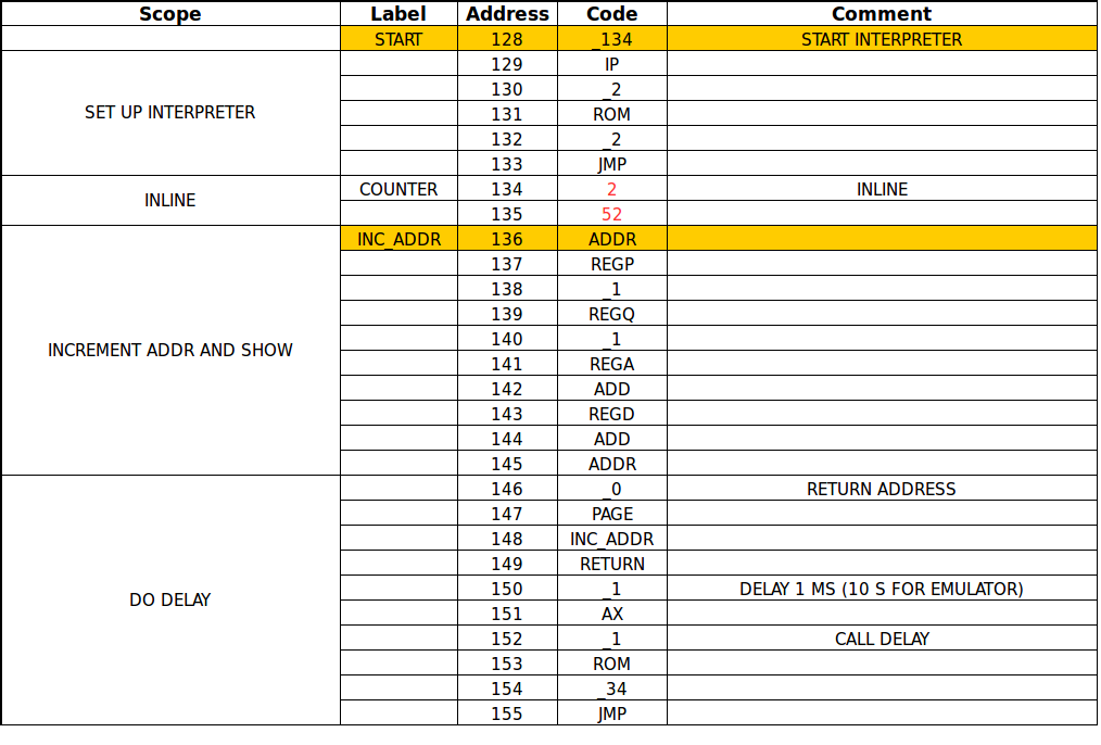
Here is the Interpreter (including Inline and Decode):
![]()
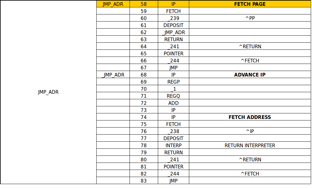
The next Interpreter instruction to write is "JMP_ADR". This will allow jumps to other pages (i.e. it sets the current Interpreter page (PP) and address (IP)). Well actually it has been written just not tested:
![]()
AlanX
-
Version 3 Emulator
06/28/2018 at 10:18 • 0 commentsWhats New?
- Coded a second ROM page.
- The monitor code spans both ROM pages.
- The monitor is both hardware and emulator friendly (i.e. delay rountine added).
- An "Address to Page" decoder routine has been added.
- The Interpreter has been coded but not currently in use.
- The counting demo with delay is machine code.
Version 4
- The Emulater assumes read/write of registers (assumes PCBs will be reworded to suit).
- A bit of a re-organisation the Monitor code.
- Update Reset code.
- Add all the ROM and RAM pages.
- Add code to the Monitor to change RAM pages (uses PAGE PTR), until PCB boards have been updated for register read/write.
- Coded the Interpreter and some support subroutines (ROM PAGE 2).
- Add PP (Page Pointer) to keep track of the Interpreted Page.
- The Interpreter still to be tested.
![]()
The Emulater itself is now pretty complete.
AlanX
-
Second Pass Emulator
06/26/2018 at 11:58 • 0 commentsSecond Pass Emulator
The second pass recoginises the I/O or ports are accessed via:
- REGA - the port address
- REGD - the port read/write
The third pass will add paged RAM and ROM.
Run out of room
Run out of room for the monitor, well I ran out of room a while ago when I "stubbed" the delay routine. Anyway I need to push some code onto ROM page 1 (i.e. the second page).
One of the monitor design "features" was to hide the ROM and RAM page registers from the front panel.
The problem is you cannot manually change the ROM page with monitor running.
The monitor should really have no reason to view the ROM code (on another ROM page) in any case.
Changing the RAM page would be okay, however. But the current design does not allow you to read the page registers and I have no pull ups (or pull down resistors on the Databus. So even changing RAM page is messy.
One way to read/write from/to a register and then copy that register to the RAM page at the end of the monitor rountine. Extra code is the cost for tis patch.
Checking the Page Memory Board schematic:
![]()
I need to add three chips (a decoder and two registers) for a total of 13 chips (crowded).
May be better to split the board into Page ROM and Page RAM.
I should have added pull up resistors to the Program Counter Board:
![]()
It is no big deal, you should not be using the monitor to probe around in this area anyway as it will result in strange things happening as it may interfere with the monitor.
Progress
Anyway, the monitor code is progressing, but ever so slowly.
Version 3 will consider ROM/RAM paging (and require a significant code rework).
Okay I have a plan!
First what was the problem? Oh yeah, two paging systems and how to bring them together for the Interpreter.
Basically an "Instruction Address" has the format:
- Address
- Page
But the Page may be ROM or RAM or the static System area.
The answer is to look at the Address:
- 11XX XXXX System area (registers and static RAM)
- 10XX XXXX RAM Page
- 0XXX XXXX ROM Page
The code would look like this:
        POINTER ; Get the Address
        REGP
        _64     ; Test if 11xx xxxx (System area)
        REGQ
        _EXIT   ; Exit if System area
        JC
        _128    ; Text if 10xx xxxx (RAM Page area)
        REGQ
        _NEXT   ; Goto RAM Page
        JC
        PAGE    ; No, its ROM Page (0xxx xxxx)
        ROM
        _EXIT
        JMP
_NEXT:
        PAGE
        RAM
_EXIT:
So expensive for the Interpreter but what choice do I have? Without the issue of Page addressing the Interpret would look like this (5 machine instructions or 10 bytes):
INTERP    IP      ; SAVE IP
          POINTER
          IP      ; INC IP
          REGP
          _1
          REGQ
          ADD
          IP
          _246    ; ^POINTER
          JMP
With ROM Paging ONLY (no Address decoding) it would look like this (8 machine instructions):
INTERP    IP      ; SAVE IP
          POINTER
          IP      ; INC IP
          REGP
          _1
          REGQ
          ADD
          IP
          IP      ; GET ROM PAGE
          ROM
          IP      ; INC IP
          REGP
          ADD
          IP
          _246    ; ^POINTER
          JMP
With Address decoding (17 machine instructions):
INTERP    IP      ; SAVE IP
          POINTER
          IP      ; INC IP
          REGP
          _1
          REGQ
          ADD
          IP
          IP      ; GET ROM PAGE
          PAGE

;         PAGE ADDRESS DECODING
          POINTER ; GET ADDRESS
          REGP
          _64
          REGQ
          _EXIT   ; SYSTEM AREA
          JC
          _128
          REGQ
          _RAM    ; RAM PAGE
          JC
          PAGE    ; SET ROM PAGE
          ROM
          _EXIT
          JMP
_RAM      PAGE    ; SET RAM PAGE
          RAM
_EXIT     _1      ; RESTORE REGQ
          REGQ

; CONTINUE WITH INTERPRETER
         IP       ; INC IP
         REGP
         ADD
         IP
         _246     ; ^POINTER
         JMP
If you find the code above incomprehensible then you can understand why micro-coding is so slow and why an Interpreter is so important.
AlanX
8 Bit TTA Interpreter
TTA (Transport Triggered Architecture) is very simple CPU type.