-
Memory and Instruction Fetch
06/14/2018 at 11:00 • 0 commentsMemory and Instruction Fetch
Here are some Logisim subcircuits representing parts of the machine
concerned with memory, instruction fetching and instuction decoding.Main Memory
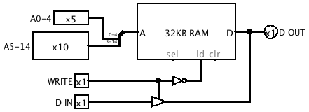
![]()
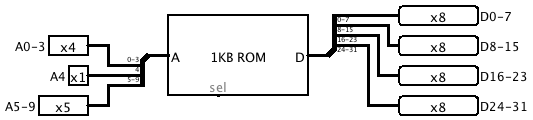
Although the memory in the final machine will be dynamic, I'm modelling
it with a Logisim static memory component for now. The memories I
intend to use have asynchronous write with separate data inputs and
outputs. but Logisim doesn't provide that combination directly, so I
emulated it using a tri-state buffer.I split out the address bus inside the subcircuit into bit number
(A0-A4) and short word number (A5-A14) parts, to make the main circuit
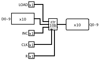
clearer.Program Counter
![]()
The Program Counter is a 10-bit counter with Increment and Load capabilities, both synchronous.
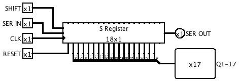
S Register
![]()
The S Register is an 18-bit shift register. The most significant 17
bits are available as parallel outputs for loading into the Instruction
Register.Why the most significant rather than the least significant? That's a
good question! It's because the Instruction Register will be loaded
during the last clock period of a memory read cycle, when the most
significant bit hasn't yet been shifted in. Therefore, at that time,
bits 0-16 of the instruction word will be in bits 1-17 of the S
Register.Instruction Register
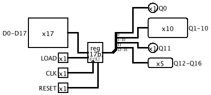
![]()
The Instruction Register is fairly simple -- it's just a 17-bit
register with synchronous parallel load. The subcircuit splits the
output into instruction fields: Length (0), Address (1-10) and
Opcode (12-16). (Bit 11 is currently unused.)Microcode ROM
![]() There's not a lot to see here either. I'm not sure exactly how wide the microcode will need to be, I've made it 32 bits for now.
There's not a lot to see here either. I'm not sure exactly how wide the microcode will need to be, I've made it 32 bits for now.Bits 4-9 of the microcode address will come from the instruction, and
bits 0-4 from the State Counter. Thus, each combination of Opcode and
Length will select a line of microcode with room for up to 16
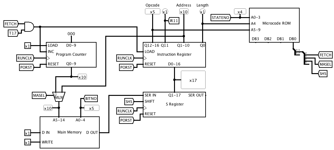
microinstructions.Putting it together
![]()
Here's how it goes together so far. Fetching an instruction is
accomplished by setting FETCH = 1, MASEL = 0 and SHS = 1. This causes
the main memory address to be taken from the Program Counter, and data
read from the memory to be shifted into the S Register. FETCH together
with T17 causes the Instruction Register to be loaded from the S
Register, and also increments the Program Counter ready for fetching
the next instruction. -
Timing Chain
06/13/2018 at 07:08 • 0 comments -
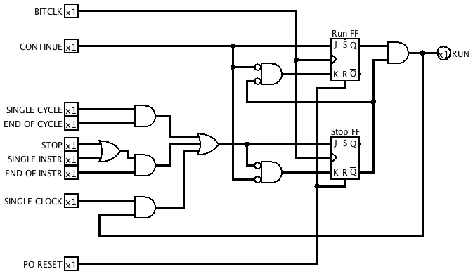
Run Control Update
06/12/2018 at 10:58 • 0 commentsI've made a change to the Run Control circuit. The way it was, pressing Stop would cause the machine to stop in the middle of an instruction, which wasn't the intention.
Here's the revised circuit. The STOP input is now connected to give the same effect as SINGLE INSTR mode, so that stopping does not occur until the end of an instruction.
![]()
-
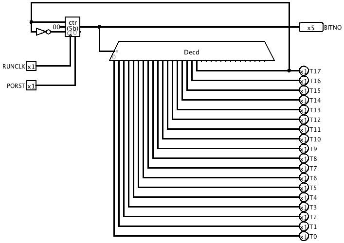
Logisim Model - Bit and State Counters
06/11/2018 at 12:08 • 0 commentsBit Counter
The Bit Counter is a 5-bit counter that is wired to count up to 17 and
then reset to 0. A decoder produces outputs corresponding to each bit
of the short word cycle.![]()
State Counter
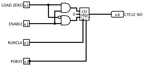
The State Counter is a 4-bit (for now) counter. When the ENABLE input
is active, it either counts up (if LOAD ZERO is inactive) or is reset
to zero (if LOAD ZERO is active). When ENABLE is inactive, no state
change occurs.![]()
-
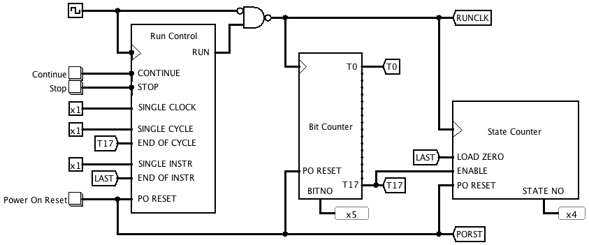
Logisim Model - Run Control
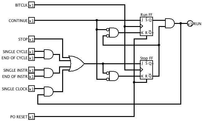
06/10/2018 at 13:34 • 0 commentsBefore building any hardware, I'm going to model the CPU using Logisim
to test out the design.Here's the first part, the Run Control circuit. Its purpose is to take
signals from the front panel controls for starting and stopping the
machine, together with some signals derived from the machine's state,
and generate a RUN signal that is active whenever the machine should be
running. This signal will be used to gate BITCLK pulses to the rest of
the machine, so its transitions need to be aligned with BITCLK period
boundaries.![]()
CONTINUE and STOP will be connected to pushbuttons on the front panel.
(In the original EDSAC, CONTINUE was named "Reset", but I've renamed it
to avoid confusion with the power-on reset signal.)SINGLE CYCLE, SINGLE INSTR and SINGLE CLOCK are mode-selection
inputs that will be connected to switches of some kind. END OF CYCLE
and END OF INSTR are internal signals that will be active during the
last clock period of a short word cycle or a complete instruction
respectively.At power up, the PO RESET signal resets both flip flops so that RUN is
initially inactive.When the CONTINUE button is pressed, on the next rising edge of BITCLK
the Run FF becomes set and RUN becomes active. In continuous-running
mode (none of the SINGLE X inputs are active), RUN remains active until
the STOP button is pressed. The Stop FF then becomes set on the next
rising clock edge, which deactivates RUN via the AND gate. This
condition persists until both CONTINUE and STOP are released, whereupon
both flip flops are reset and the machine is ready to be started again.The SINGLE X modes provide alternative ways of stopping the machine.
For example, in SINGLE INSTR mode, the machine will run only until END
OF INSTR becomes active, and then will be stopped just as if the STOP
button had been pressed. The dual flip-flop arrangement ensures that
another instruction will not be executed until the CONTINUE button has
been released and pressed again.You can see a video of the Run Control circuit working here.
-
Block Diagram
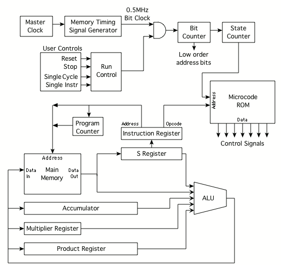
06/07/2018 at 10:42 • 0 commentsHere's a block diagram of the overall organisation I have in mind.
![]()
The Memory Timing circuit produces control signals for the dynamic RAM
and divides the master clock down to 0.5MHz. This is gated by the
output from the Run Control circuit to produce the bit clock for the
rest of the machine.The Bit Counter counts from 0 to 17, representing one short word cycle.
Its output is used as the low-order address bits for both the main
memory and the memories holding the register values.One microinstruction is executed during each short word time, after
which the State Counter is incremented to move on to the next
microinstruction (unless a microbranch causes it to be loaded with a
different value). The output of the State Counter forms the low order
bits of the microinstruction address, with the high order bits taken
from the opcode bits of the instruction being executed. I'm currently
planning on using a 4-bit state number, allowing for up to 16
microinstructions per machine instruction. This ought to be more than
enough, but it can be increased if the need arises.The Program Counter is 10 bits wide and keeps track of the next machine
instruction to be executed. The word address for the main memory comes
from either the Program Counter or the address field of the Instruction
Register.The S Register is a 17-bit shift register that does not have an exact
equivalent in the original machine. It performs serial-to-parallel
conversion of instructions read from main memory, and will also hold
one of the operands during a multiplication (which is why there is no
Multiplicand register in the diagram).The Product Register did not exist in the original machine. It will be
used to build up the result of a multiplication before adding it to or
subtracting it from the accumulator.The ALU will be capable of Add, Subtract and Logical And operations, as
well as passing one operand through unchanged or generating a constant
output of zero. Inputs can come from the main memory, the accumulator
and the S, Multiplier and Product registers. The result can be written
to the main memory, the accumulator, and the Multiplier and Product
registers.Outputs from the Microcode ROM control the functions of all the other
parts of the machine, including loading of registers, selecting inputs
to the ALU, selecting the function performed by the ALU, and writing to
registers and memory.I/O devices are not included on this diagram, as I haven't decided exactly how they will fit in yet.
Also not included is the system responsible for refreshing the main
memory and generating the oscilloscope displays of memory and register
contents. This will be an autonomous unit that operates entirely
independently of the computational logic. -
Timing
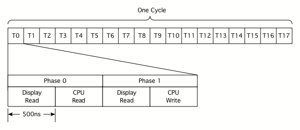
06/02/2018 at 09:52 • 0 commentsBREDSAC will operate on an 18-bit basic cycle, corresponding to a short word.
Because some operations require reading and writing back to the same
register, each bit time will be divided into two phases. In the first
phase a read may occur, and in the second phase a write may occur.To allow for generation of the memory and register oscilloscope
displays, each of these phases will be further divided into two
subphases, one for the display system and one for the CPU.![]()
The RAMs I'm using for the main memory and registers both have a cycle
time of 500ns, giving a bit time of 2us. Coincidentally, this is the
same as the bit time of the original EDSAC. However, the EDSAC had a
variable memory access time due to the need to wait for the word you
wanted to come around in the delay line, which could take as long as 32
short word times, or 1.152ms. The BREDSAC, with truly random access
memory, will be considerably faster. -
Preliminary design thoughts
06/02/2018 at 07:43 • 0 commentsTechnology Level
I want to make use of parts from my junk box wherever possible, which
means largely using 74 series TTL and parts from a similar era. Any new
parts that I buy will probably be 74HC, as TTL is becoming hard to get
these days.There will be no microcontrollers or other ready-made programmable parts -- that would be cheating.
Serial or Parallel?
In keeping with the spirit of the original, and to keep the part count
down to something reasonable, BREDSAC will be a serial machine. While
this means it won't be blazingly fast, it will still probably be quite
a lot faster than the original -- more on that later.Memory
For the memory, I intend to use a pair of 16k x 1 bit dynamic RAM chips
(4116 or equivalent). Why dynamic rather than static? Various reasons.
Serial operation means that a 1-bit wide RAM makes the most sense, and
the only sufficiently large 1-bit memory chips I have lying around
happen to be dynamic. It provides an excuse for the word BREDSAC to
have a D in it. The EDSAC used mercury delay lines for its memory,
which also needed continuous refreshing, so it's kind of authentic. And
apparently I don't like to make things too easy for myself. :-(The use of dynamic memory will have a side benefit. As a by-product of
the refresh process I should be able to derive a signal that I can send
to an oscilloscope to produce something very like the original EDSAC's
CRT memory display.Registers
There are a couple of ways I could go about implementing the registers.
The most obvious would be to use shift registers. This would be the
most similar to the way the original machine operated, and if I use
serial-in parallel-out types it would be very easy to display the
contents of the registers by connecting LEDs to the outputs. However,
it would require a lot of parts -- 71 bits for the accumulator plus
another couple of 17-bit registers would add up to about 15 or so chips.Another possibility would be to use RAMs. I have some 1k by 1 bit
static RAM chips, one of which would be enough to hold all the required
data, although I would probably use two or three to allow for
simultaneous access to multiple registers. The disadvantage is that it
wouldn't be so easy to display register contents, but should be
possible to generate an oscilloscope display of the memory holding the
registers much the same way as with the main memory. This would also be
very authentic-looking.For now I'm going with the static RAM design, although I might change my mind later.
Bootstrapping
I actually have a few genuine uniselectors, but nowhere near enough of
them to recreate the original EDAC's method of loading the initial
orders. Unless I come up with some other hare-brained scheme, I'll
probably be using an EEPROM.I/O Devices
I have a real 5-bit teleprinter, although it uses a completely
different character encoding from the original EDSAC, so some kind of
translation would be needed in between. It's also extremely noisy, so
while I might try to get it working as a proof of concept, I will
probably arrange something else as an alternative, such as maybe a DEC
VT52 or a Commodore 64 (both of which I also happen to have... yes, I
have far too much junk.)I don't have any paper tape equipment, though, and the prospects of
acquiring any at any kind of realistic cost appear very slim, so I plan
to build an optical tape reader, and prepare tapes for it by a process
involving a relatively modern computer, a laser printer, a guillotine
and some sticky tape.On the plus side, I have a genuine telephone dial of about the right
vintage that there shouldn't be any problems incorporating. It will
doubtlessly be the most authentic part of the whole project. -
About EDSAC
06/02/2018 at 07:41 • 0 commentsThis is a very brief description of the EDSAC architecture. Much more information can be found in the references listed below.
Memory
The main memory consists of 1024 words of 18 bits each. It can be
accessed as short words of 17 bits or long words of 35 bits (one bit of
each word being unused for timing reasons).Registers
Name Size Usage Program Counter 10 bits Address of next instruction to be executed Accumulator 71 bits Holds results of arithmetic and logical operations Multiplier 35 bits Holds one of the operands for a multiplication The original machine had some other registers that are not listed here
beause they were not directly visible to the programmer. It is possible
that they will not have direct equivalents in my version.Data Formats
Short and long words can represent integers or fractions. Fractional
numbers are assumed to be in the range -1 <= x < 1, with an
implied binary point between the sign bit and the most significant bit.
Negative numbers use two's-complement representation.Additions, subtractions and logical operations operate on the most
significant 17 or 35 bits of the accumulator. Multiplication assumes
both operands are fractions as above. Short multiplication produces a
35 bit result, and long multiplication produces a 71 bit result.Instruction Format
All instructions occupy one short word and have the following fields.
Field Opcode Spare Address Length Bits 5 1 10 1 The Opcode indicates the operation to be performed. Many of the
opcodes are chosen to have mnemonic value when interpreted as 5-bit
teleprinter character codes (e.g. "A" = add).The Spare bit was unused in the original (1949) version of the machine.
The Address field contains the absolute address of the operand in memory.
The Length bit indicates whether a short word (0) or a long word (1) is
to be operated on. Long words occupy an even-odd address pair with the
least significant half at an even address.Instruction Set
Notations used in this table:
n Address field of the instuction C(n) Contents of memory location n f Length indicator k A shift amount, encoded by setting bit number k-1 of the instruction Instruction Description A n f Add C(n) to the accumulator S n f Subtract C(n) from the accumulator H n f Load C(n) into the multiplier register V n f Multipy C(n) by multiplier and add result to accumulator N n f Multipy C(n) by multiplier and subtract result from accumulator T n f Transfer accumulator to memory location n and clear the accumulator U n f Copy accumulator to memory location n C n f Logical AND ("collate") C(n) with contents of accumulator and add result to accumulator R k Shift accumulator right (see below) L k Shift accumulator left (see below) E n If accumulator is positive or zero, jump to location n G n If accumulator is negative, jump to location n I n Read a character from paper tape into the least significant 5 bits of location n O n Print character in the most significant 5 bits of C(n) X No operation Y Round the accumulator to 34 bits Z Halt I/O Devices
The following devices were attached to the EDSAC for input and output.
- A 5-bit paper tape reader for input
- A 5-bit teleprinter or paper tape punch for output
- A telephone dial
To read input from the telephone dial, the machine was halted with a Z
instruction. Dialling a digit caused it to be added to the accumulator
and the machine restarted.A bank of uniselectors was used to load the "Initial Orders" (boostrap in today's terminology) into main menory.
There were also some cathode ray tubes capable of displaying register
values and the contents of parts of the main memory. These were mainly
for diagnostics, but the memory display could be used as a simple form of bitmap output.Operator Controls
Clear Button Clears all registers and main memory locations Start Button Loads the Initial Orders into memory and begins executing them Stop Button Manually stops execution Reset Button Continues execution from where stopped References
EDSAC Simulator for Windows - includes documentation providing more architectural details.
The Preparation of Programs for an Electronic Digital Computer - lots of very detailed information about a later version of the machine.
The EDSAC Wikipedia article lists many other useful references.
 There's not a lot to see here either. I'm not sure exactly how wide the microcode will need to be, I've made it 32 bits for now.