 Torbjörn Lindholm
The aim of this project is to explore the following topics:
- Use of SMD components
- Double-sided PCB making
- PCB art (Odd shaped circuit boards)
- ESP8266
- Programming
- Packing boards together for manufacturing
- Miniaturization
- Using KiCAD
- Not to mention fun
Disclaimer:
All materials (logo, symbol, typeface) are ® and ™ of CD Projekt S.A. and associated parties.
Author and/or this project is in no way sponsored, endorsed or affiliated by CD Projekt RED or CD Projekt S.A.
Not for sale. Personal and nonprofit use only. CC-BY-NC-SA.
For people who are going to distribute the finished board (which I assume isn't going to be many):
There must be absolutely zero monetary transaction while you distribute the boards. Do not remove "NOT FOR SALE" text. Keep in mind that this is using a copyrighted material as a part of fan project.
All materials are generated using KiCad and Adobe Illustrator CS6 using JLCPCB's design rules for ease of manufacture as it seems to be an industry standard rule-set.
About Components & Assembly
For the MOSFETs, make sure the pin 1 is Gate and pin 2 is Drain. Make sure the gate threshold voltage is lower than 3.3V and make sure it can withstand at least 200mA. (single-cell lithium battery protection boards use this part)
The crystal oscillator on the daughterboard needs to be affixed to the pad right behind it to prevent excessive vibration and temperature fluctuations.
The battery needs to support at least 250mA of sustained load and must have voltage rating of at least 4.2V.
There should be some marks to indicate what to do - such as signs which look like these:
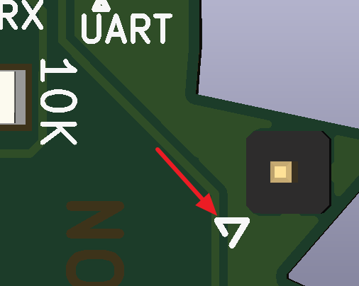
There are two sets of symbol and an extra to show if you did it wrong:
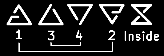
Match the symbols on the board in that order and it should work just fine. All symbols should not be visible from outside when it's finished.
The power switch has been placed inside to prevent accidental activation, and reset and program switch has been placed near the edge of the board so it's not pressed when not required. You can press and hold respective buttons with a spudger, screwdriver or any stiff object.
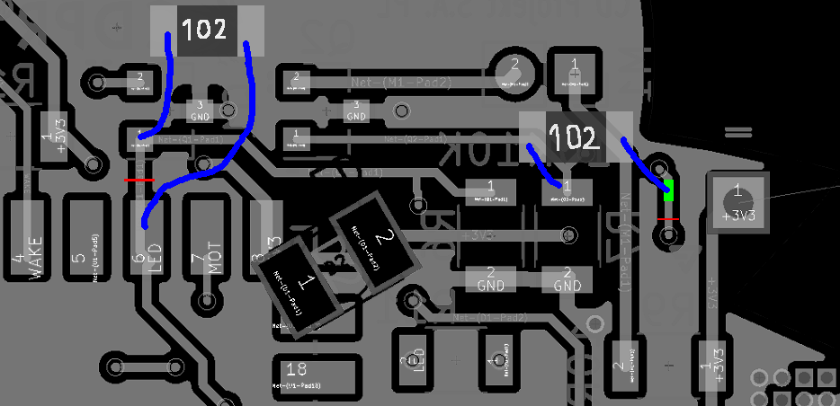
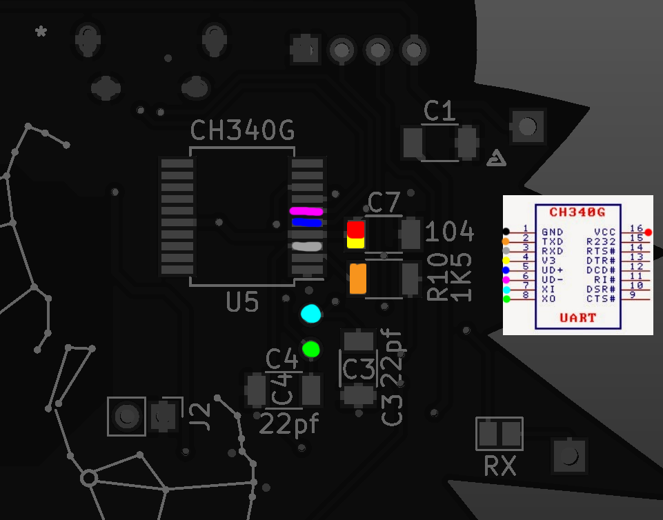
Bridge the RX and TX jumper to enable the daughterboard's CH340G chip, or leave it alone to use external programmer.
By bridging U_PWR jumper, you can power this board with the USB connection. Else, you can use external power through the top UART port.
There are places where a mouse symbol is shown -- these are places where you can break the board off. Using side cutter or a knife cut or score the perforated edge and snap the board apart. Use file to smooth the rough edge down and add some nail varnish or resin to seal the edge.
Before continuing, wash the board with isopropyl alcohol (or rubbing alcohol) to wash off any residual chemical from manufacturing process. This is what is gonna be on your skin, after all. You don't want any copper salt, lead salt or any of the acid used in the process getting on your chest or your hands.
You can either hand-solder or use reflow oven and solder paste to assemble the board. (order SMD stencil if you are making more than 2)
Make sure the components are not falling off when soldering the other side; It's not fun to fix these kind of problems. For cheaper boards with maximum rating of 140 degrees centigrade, You must use low-temperature solder paste or hand-solder all the parts, in order to prevent the board from getting burnt.


 Neven Boyanov
 The Big One
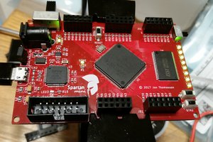
 Jon Thomasson