Pavel
Pavel-
Memory access modes
02/19/2021 at 09:06 • 0 commentsModes to have:
A. Immediate loads: values are inside instructions
B. Direct loads/stores: address is in instruction
C. Indirect loads/stores: address is in one of four Memory Pointer registers
D. Indirect loads/stores with offset: base address is in Memory pointer, while the 16-bit signed offset value is taken from General Purpose registers or from the word following the instruction
E. Indirect loads/stores with post-increment: same as C, only after memory access the memory pointer value gets incremented by value from GPR, or from the next word, or by one of pre-set values
F. Indirect loads/stores with pre-increment: same as D, but address in Memory Pointer gets updated before memory access
(probably some more?)
-- Loads and stores are to be mostly to and from General Purpose Registers.
-- Only way to load data into Memory Pointers and 8-bit registers from memory would be immediate values that are encoded into instruction.
-
Register File / Main data path design
02/18/2021 at 13:37 • 0 commentsThis is just an overview of the core number crunching component of the processor:
There are two parts to it - ALU and Register File.
ALU is described in previous log.
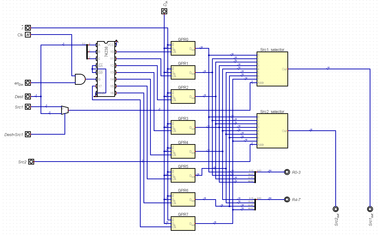
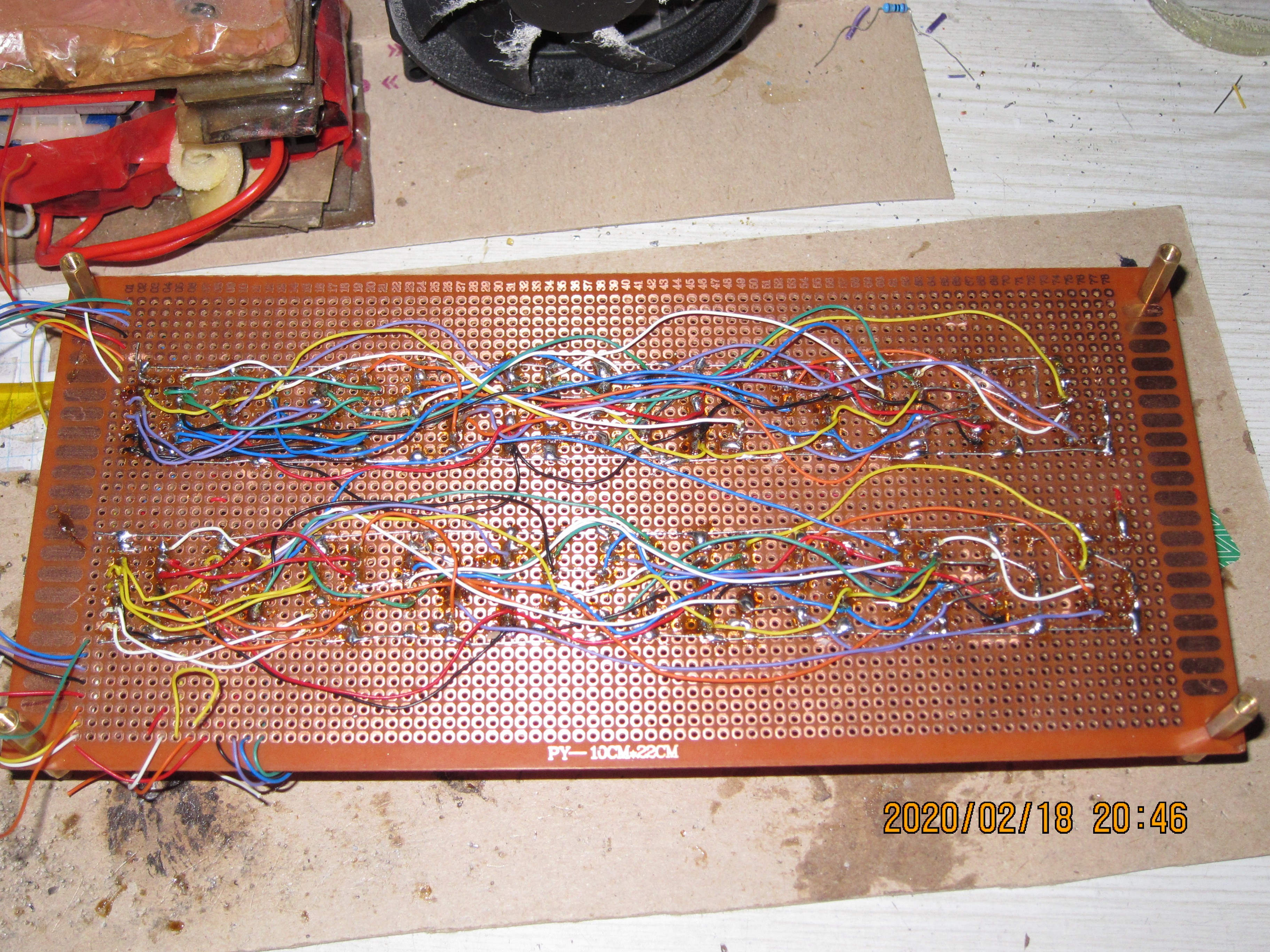
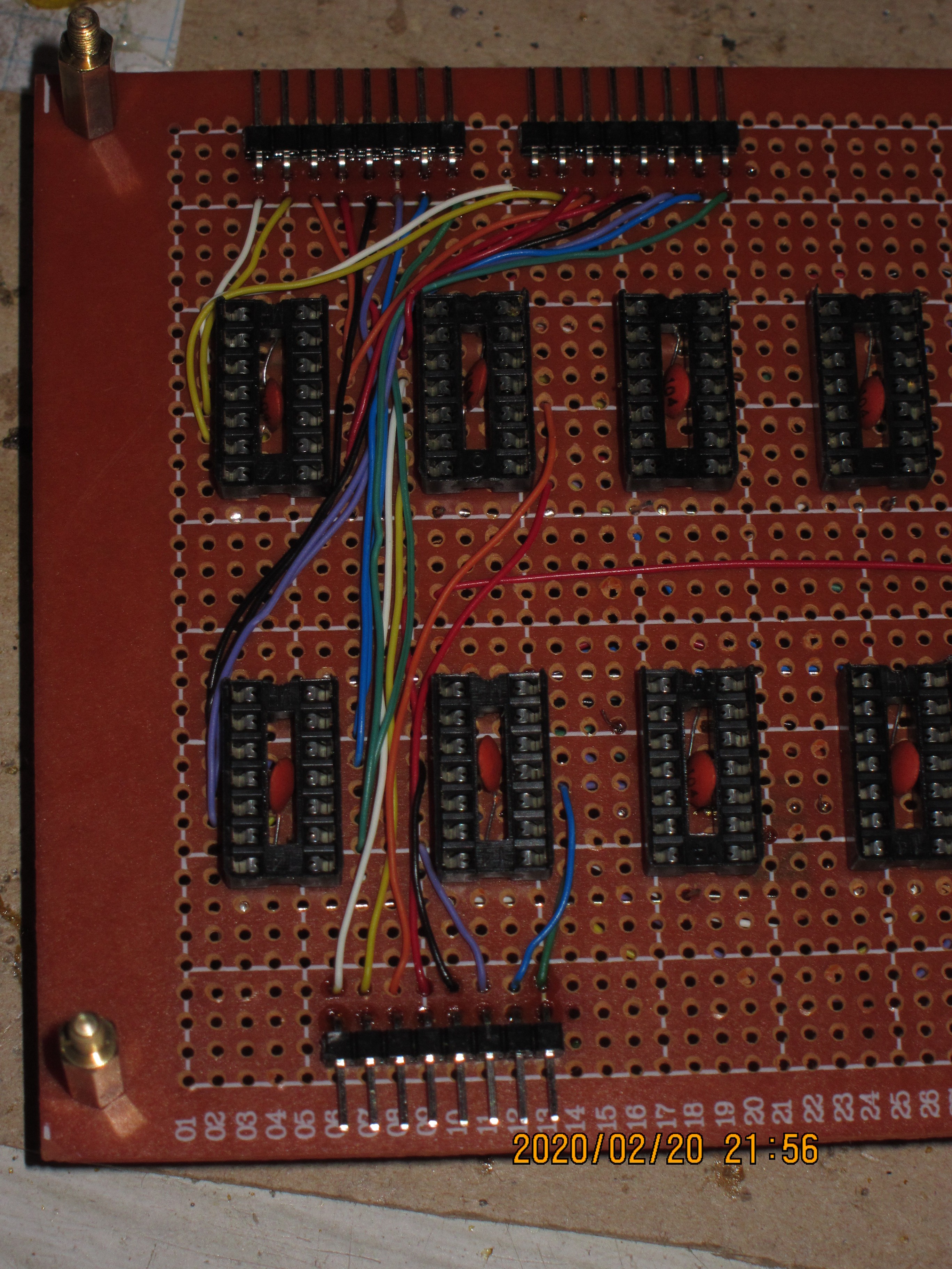
The register file combines eight 16-bit registers, 3-to-8 decoder and two 8-to-1 16-bit multiplexers. One of the registers can be selected to be written to, and at the same time, output from two others can be channelled to respective ALU inputs.
![]()
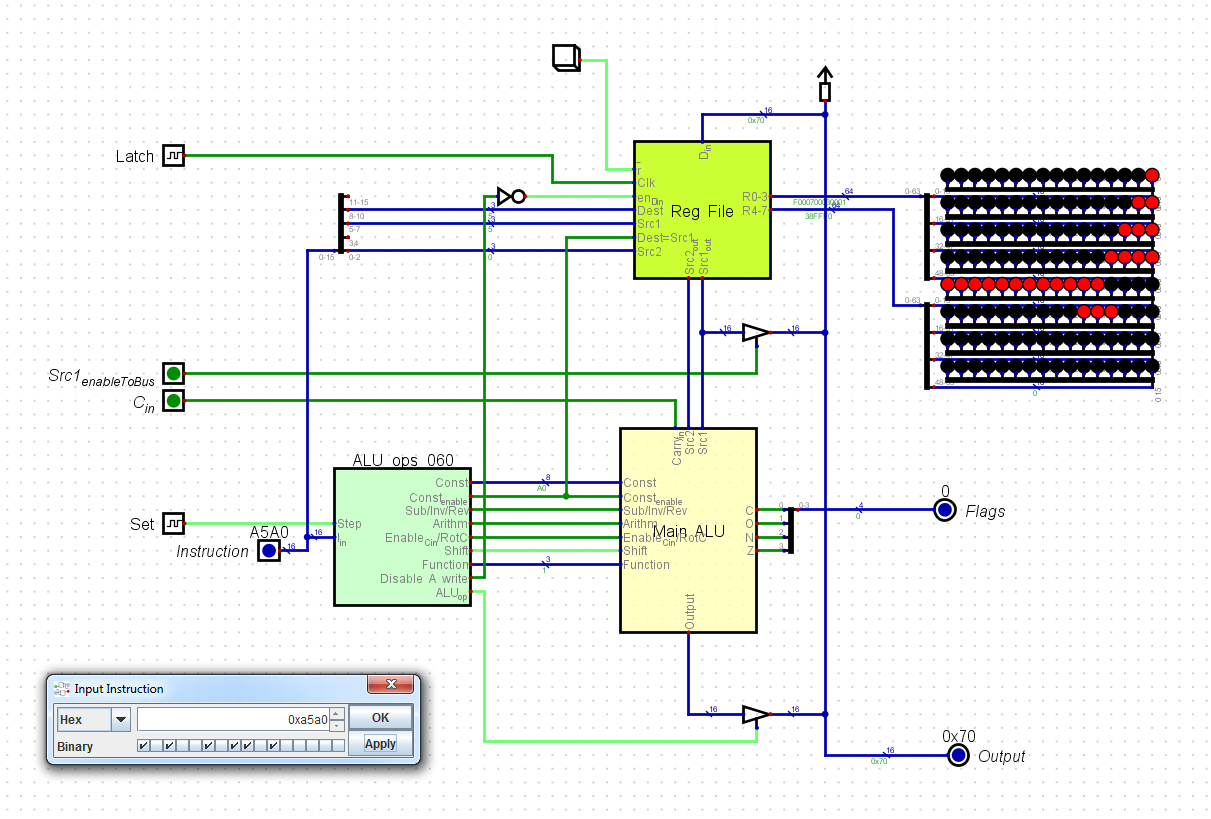
Register File acts as sort of very small memory with 8 addressable words. Together with ALU it forms what I call Main Data Path -- the computing core of the processor, which by itself is quite capable. By feeding it the right sequence of commands it is possible to do multiplications and divisions, and probably some other functions not provided by ALU right away.
Here is screenshot of it in current implementation (together with ALU instruction decoder):
![]()
-
ALU refining pt 2; updated approach to CPU design
02/15/2021 at 09:06 • 0 commentsFollowing are descriptions of design changes:
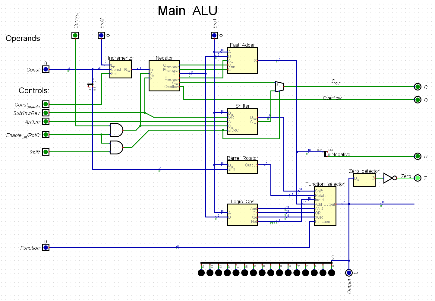
1. Some reshuffling of ALU schematic -- mainly for more clarity (compare to schematic in one of the early logs):
![]()
Most of the glue logic (individual gates controlling such things as carry flipping at subtraction) were moved to the functional blocks. The blocks themselves are redone with 74 family chip outlines to serve as the reference while building hardware -- as there were some unused pins/gates on those chips, the were repurposed for those glue logic functions.
Operation description:
There are 2 main 16-bit input busses (Src1 and Src2), one 8-bit input (Const), and one 16-bit output bus.
For some operations the 8-bit constant is switched in instead of "Src2", using the Incrementor block;
Next, the signal from "Src2" | "Const" goes through Negator block, which inverts it, alongside with "Carry_in" to facilitate subtraction.
The signals then go in parallel through 4 blocks which do different operations:
- adder takes "Src1" and (+/-)"Src2"|"Const", and outputs 16-bit sum;
- logic operations unit uses the same values as adder, and outputs results of its own operations;
- shifter works on "Src1" input and does simple and arithmetic left/right shifts and rotations through carry;
- barrel rotator also works on "Src1" input, and does rotation to the left (0 to 15 bits)
2. Slight change to command encoding - mending a couple of irregularities:
Previously, there were two ways of doing ALU functions: the one where one of the two source registers was also a destination, and the other where destination could be the third specified register. Now the first version is only used with constant value, otherwise three arguments are specified in the instruction (two sources and destination for two-operand operations).
There also was compare command which was interfering with three argument ops, where the registers 0 and 1 couldn't be used as destination. This interference is now overcome with different encoding of the compare instruction.
3. More top-down approach for overall CPU design:
When starting designing the CPU, I had no clear idea of what the addressing scheme would be, and how all its workings will be organised. The clearest ideas were that this should be 16-bit machine (16-bit data bus, and 16-bit instructions). That was dictated primarily by my assessment of possible complexities: 8-bit will have too complex addressing scheme and instruction encoding -- it most likely would be microcoded. On the other hand, 32-bit would be too much in terms of the sheer number of components needed at the level I wanted to build it (simplest logic gates). So the 16-bit seemed "the golden middle".
I wanted the machine to have a register file, a number of identical registers which are addressed in instruction, and to have an ALU capable of a adding, subtracting, logical operations and shifts, and also to have an ability to increment/decrement a value by a set number, thus a set of commands with 8-bit constant values. Overall this was constraining me to 8 registers in register file. This is also convenient, as for addressing 8 values, only one 3-to-8 decoder is needed, which a single IC.
So, the ALU and Register File were the first parts which I had fairly good idea of what I want them to be. Not the other parts. So I started with building the ALU and then Register file in simulator, and then I was adding all other parts in the order I found them necessary at the time. This led to quite a complicated mess, which incrementally grew in its ability and complexity... and in difficulty of understanding of how it all works.
That is why I am restarting almost from scratch (well, many parts are already done, they just need some tidying up), and having more holistic understanding of how I want this CPU to work I will recreate the simulation in a more clear and understandable way.
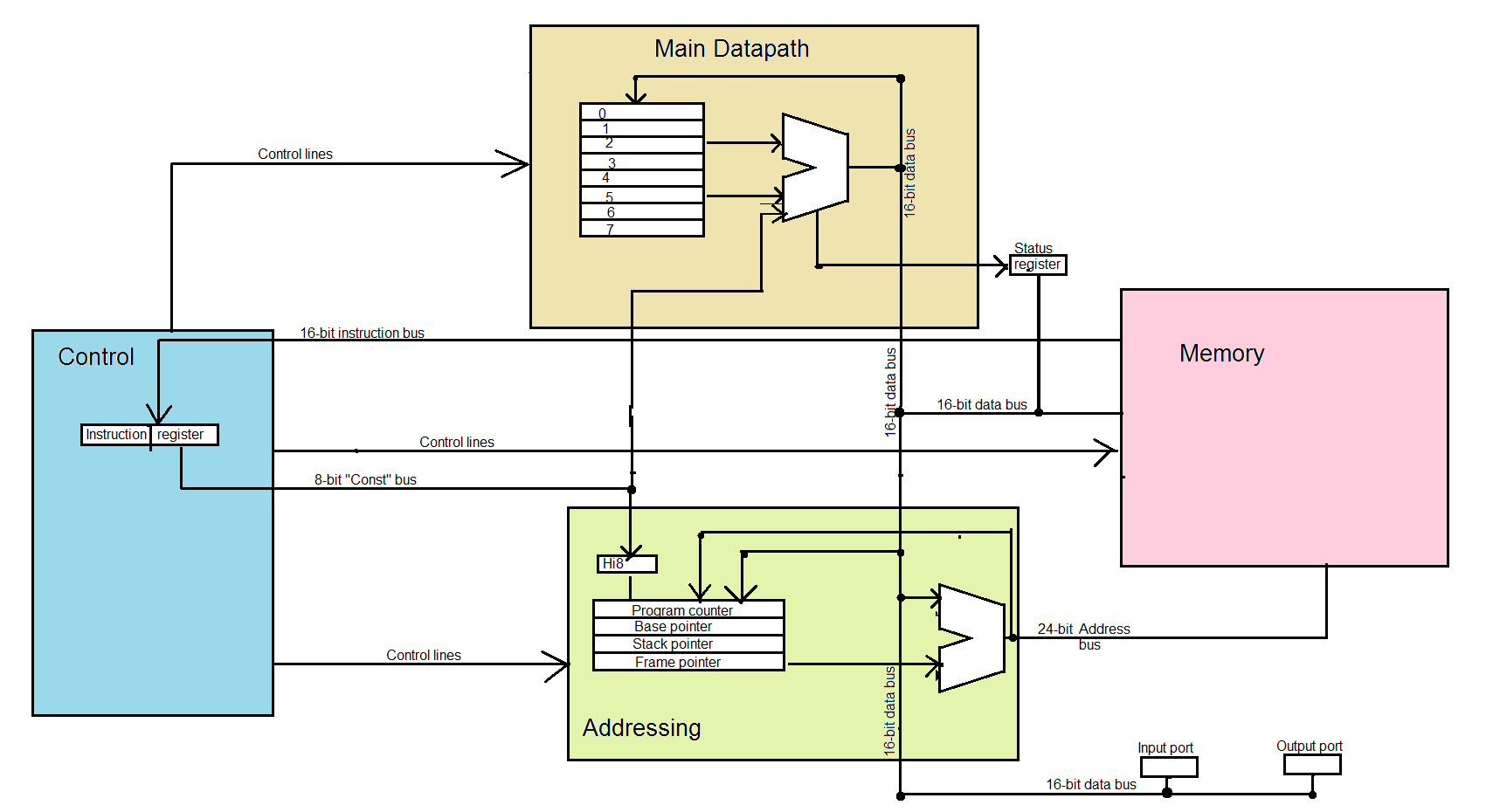
Following is the high-level scheme of CPU parts:
![]()
The scheme summarises the overall CPU design in just 4 main blocks. On a high level it is similar to what I've done up to date, just in a clearer way. The differences are in particulars, mostly in addressing block -- there the 24-bit adder is now present, and 4th 24-bit register is added (Frame Pointer). The presence of adder removes the need to make PC and SP from presettable counters, thus making design more regular.
The blocks:
- Main data path:
--- eight 16-bit general purpose registers in register file
--- main ALU (16-bit)
- Addressing
--- four 24-bit memory pointer registers ( PC, BP, SP, FP )
--- its own dedicated secondary/address ALU (24-bit)
- Control
--- Instruction Register
--- instruction decode circuitry
- Memory ( + memory-mapped input/output )
- Miscellaneous small bits:
--- four 8-bit special registers, (SR, Hi8, OP, IP), placed around the CPU.
--- Boot loading and DMA circuits.
--- Interrupt handling circuitry
--- Some other things I do not know I need yet.
-
Small boards complete
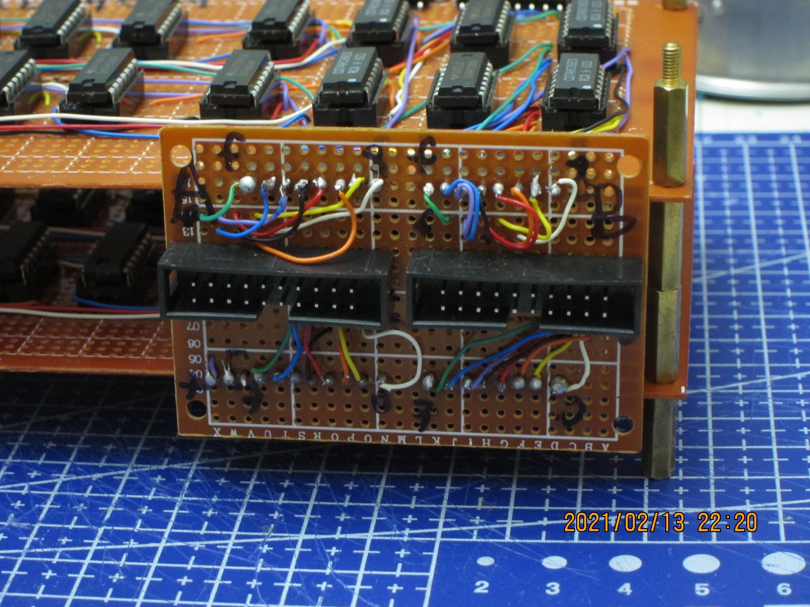
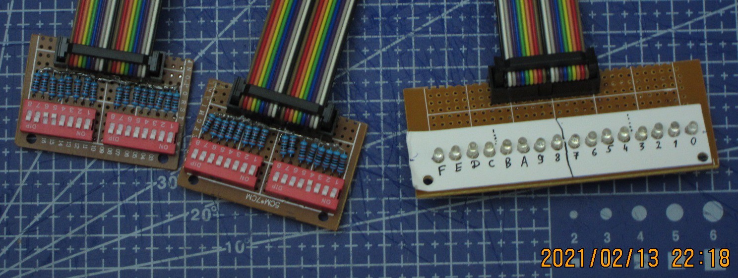
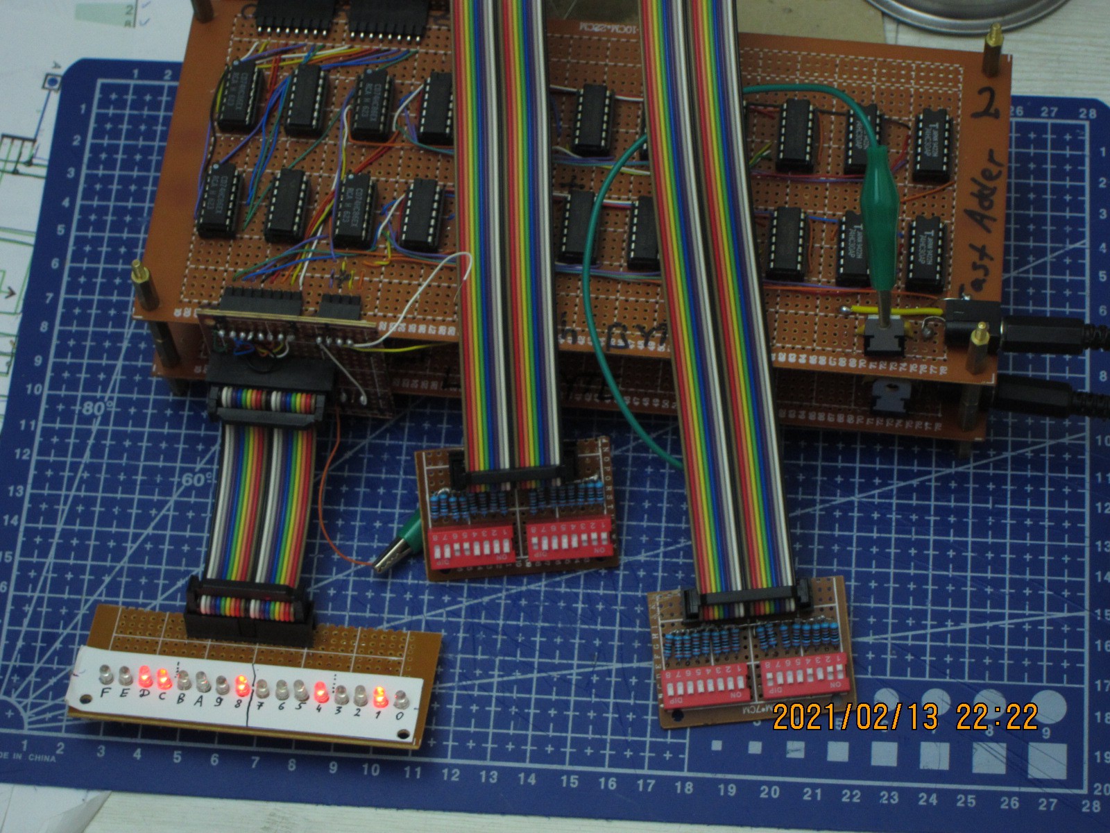
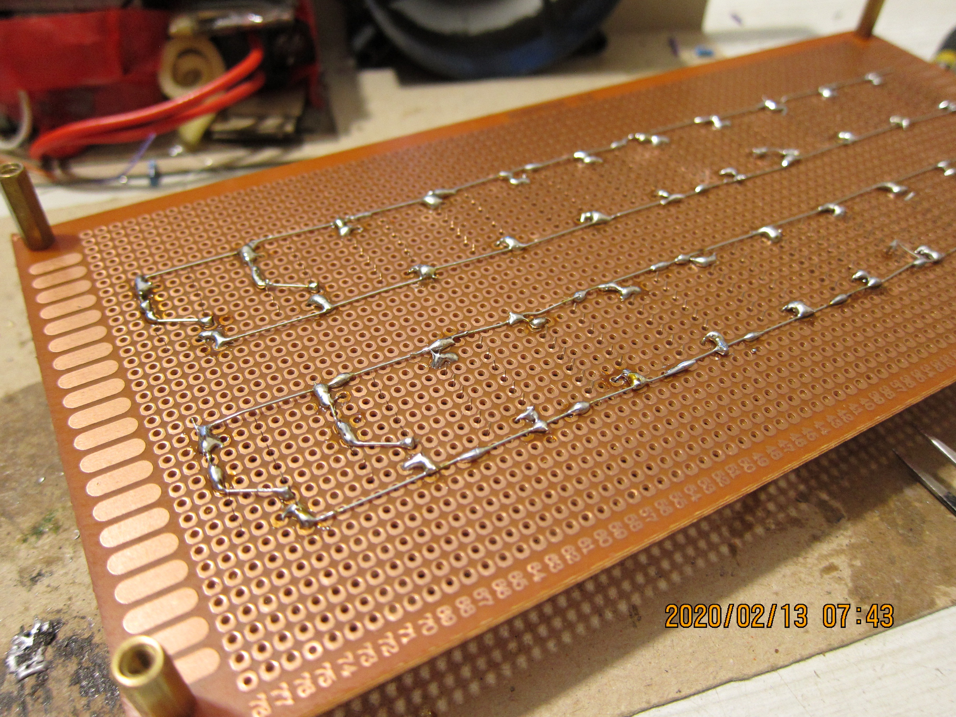
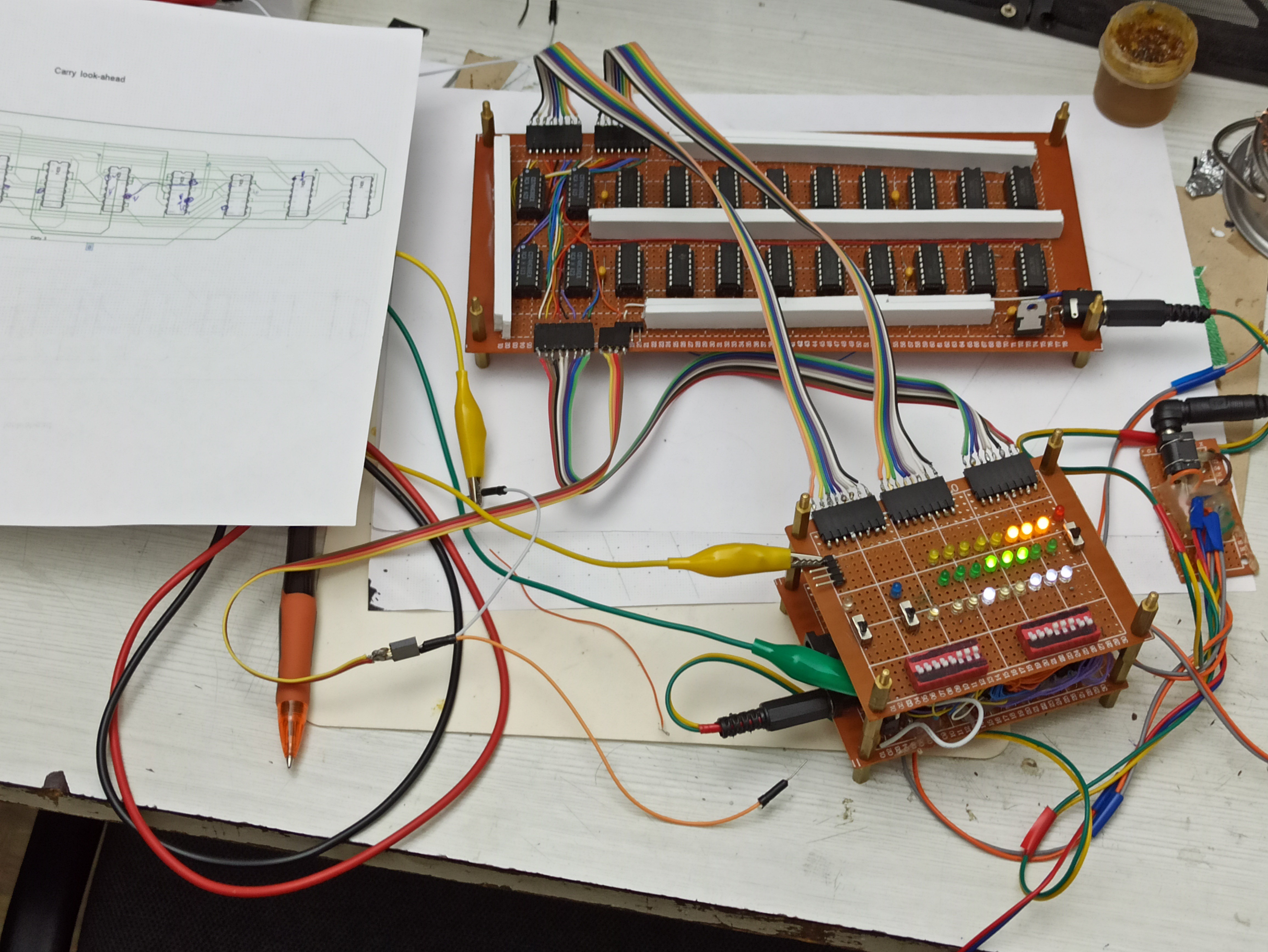
02/13/2021 at 20:56 • 0 commentsFive small boards for main ALU are completed:
1: Source1 + Source2 16-bit input adaptor for double-board fast adder
2: Output adaptor (16-bit) for double-board fast adder
3,4: Two 16-bit input boards
5: 16-bit output board (leds).
The boards were used to test 16-bit Adder unit and 16-bit Logic Operations unit. While the latter one was tested, small bug was found - there was a short in one place - and fixed.
The output adaptor ties two 8-bit adder boards via routing Carry_out signal from one board to Carry_in to other, so that they act as one 16-bit adder. Also the output and input adaptors serve some mechanical support role making the construction stiffer.
The input boards are just switch banks connected to IDC connector, while output board have 16 red LEDs connected to the same connector.
---------------------------------------------------------------------------------------
Next step will be a board combining function of the Incrementor and Negator units, and some glue logic.
Incrementor is just 16-bit 2:1 multiplexer which switches between 16-bit value from Source 2 and 8-bit constant that would be coming from the instruction word.
As for Negator - this circuit will consist of 5 74HC86 (4 x XOR) ICs, four of which are used to conditionally invert 16-bit value, and the fifth one is for the conditional invert of C_in and C_out signals.
And probably this same board could accommodate the shifter -- I am not sure, will investigate this.
---------------------------------------------------------------------------------------
Adaptor boards:
![]()
---------------------------------------------------------------------------------------
Input adaptor tied to adder boards:
![]()
---------------------------------------------------------------------------------------
Input and output boards:
![]()
---------------------------------------------------------------------------------------
Here are all these boards in action, while testing function of the adder:
![]()
-
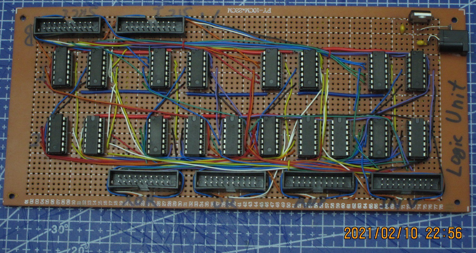
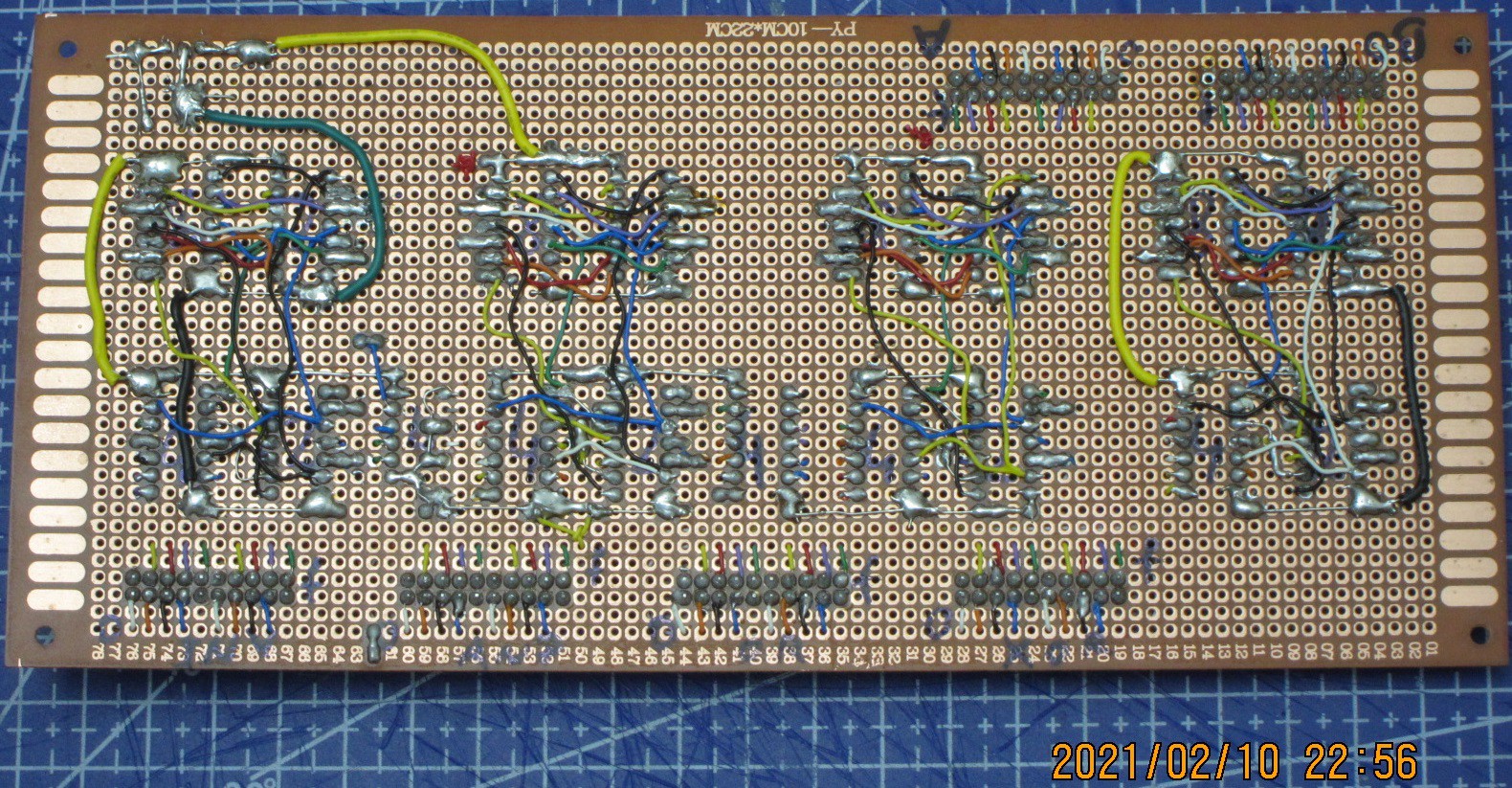
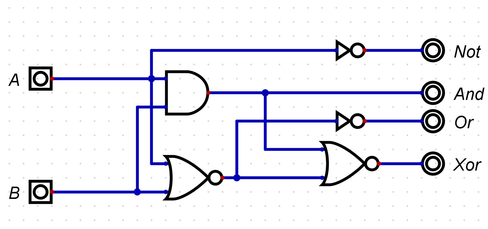
Completion of Logic Operations board
02/12/2021 at 10:27 • 0 commentsThe Logic board for the main ALU is complete. It has two 16-pin inputs and four 16-pin outputs.
Following operations are performed by the board:
1: AND (A,B);
2: OR (A,B);
3: XOR (A,B);
4: NOT (A);
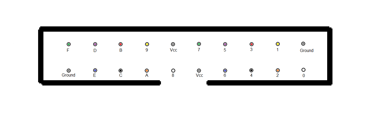
Inputs and outputs are going through 20-pin IDC connectors, with lines assigned as per following layout:
![]()
Ground and Vcc lines are used for powering passive control and indicator boards, for testing purposes. Otherwise these lines are non-functional.
Next are 5 small boards, 2 of them will connect the adder boards and add IDC connector to them, and 3 boards which will be a makeshift control panel to assess the functioning of big boards. The Vcc and Ground lines in connector layout are made specifically to support the little boards.
------------------------------------------------------------------------
This is how the Logic Operations board looks like:
![]()
![]()
Schematics:
![]()
-
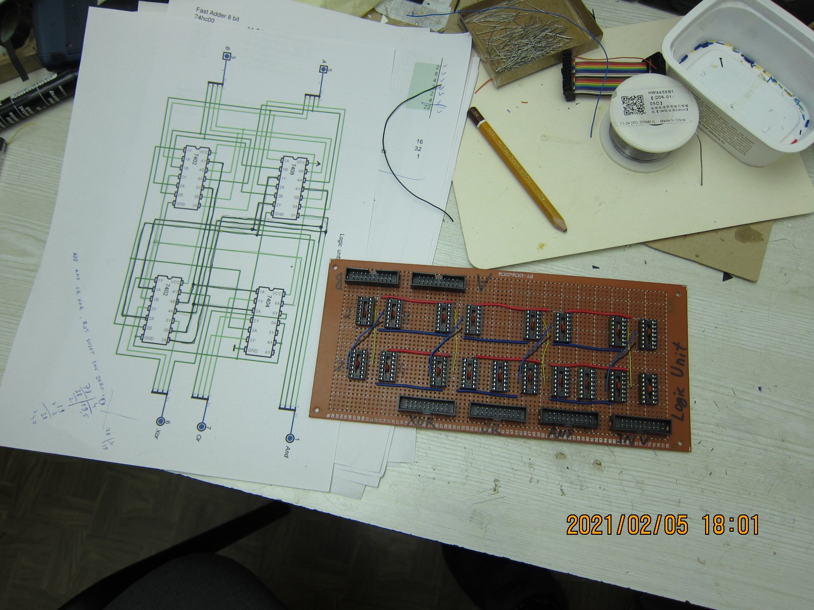
Refining the ALU
02/05/2021 at 15:31 • 0 commentsWhile soldering adders and logic unit, I took a harder look at the overall ALU schematic, and also on the instruction encoding for its operation. I seemed to me that some changes there will be despite me being certain that the design is rock-solid.
The changes to the structure will not be very big though, just a couple connections moved. As for instructions, I think there shouldn't be instructions of type A <-- op(A,B), as they are totally redundant when there are A <-- op(B,C) ones exist. Thus some instructions words become available, but to utilise them decoding logic should become more complex.
As for the other parts -- I am thinking about redoing memory subsystem from scratch, as the one in the model right now became too irregular, as it seems to me.
On the hardware front, right now work is going on soldering the Logic Operations board, which will output results of bitwise AND, OR, XOR and INV operations from its inputs:
![]()
-
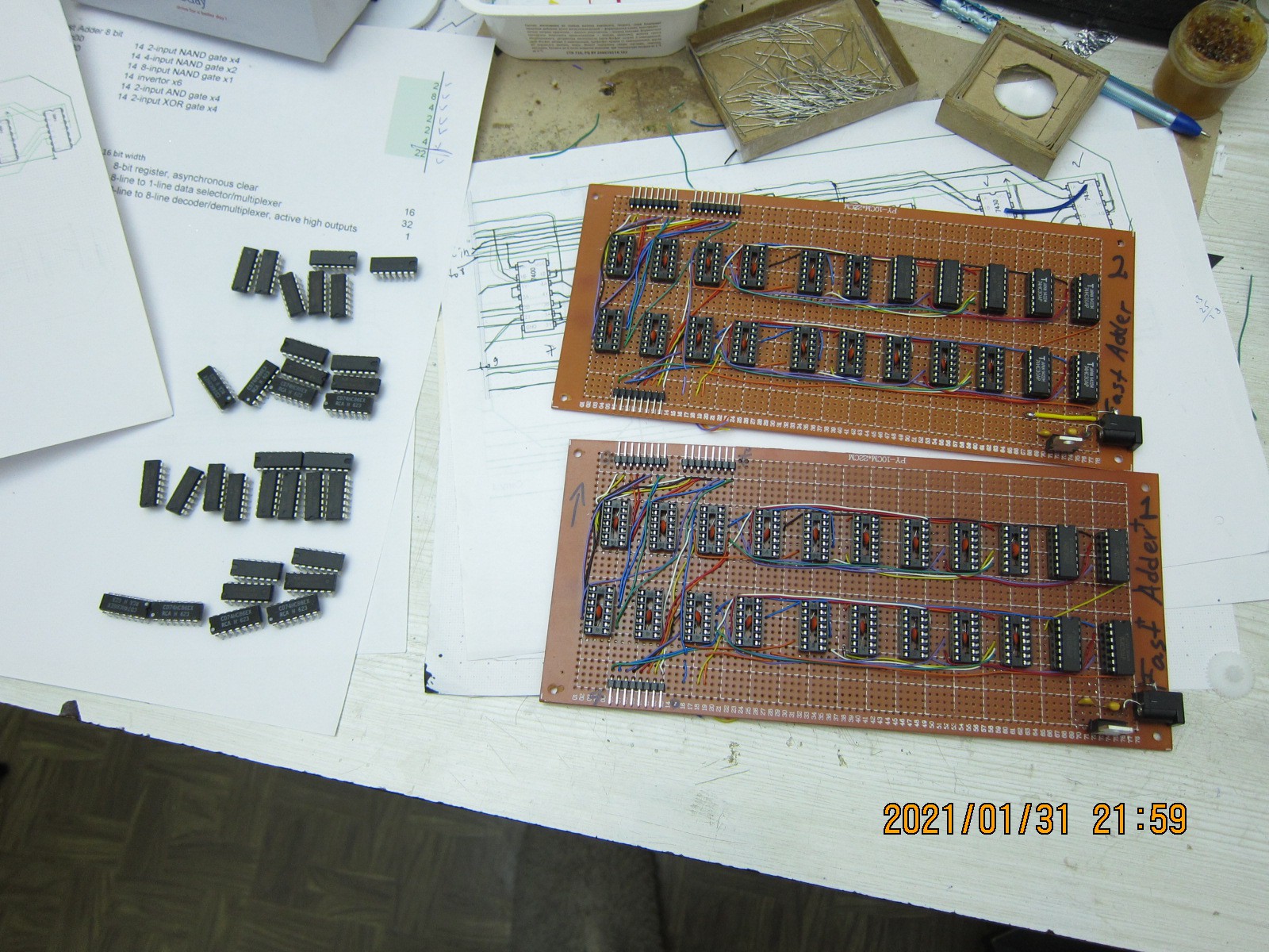
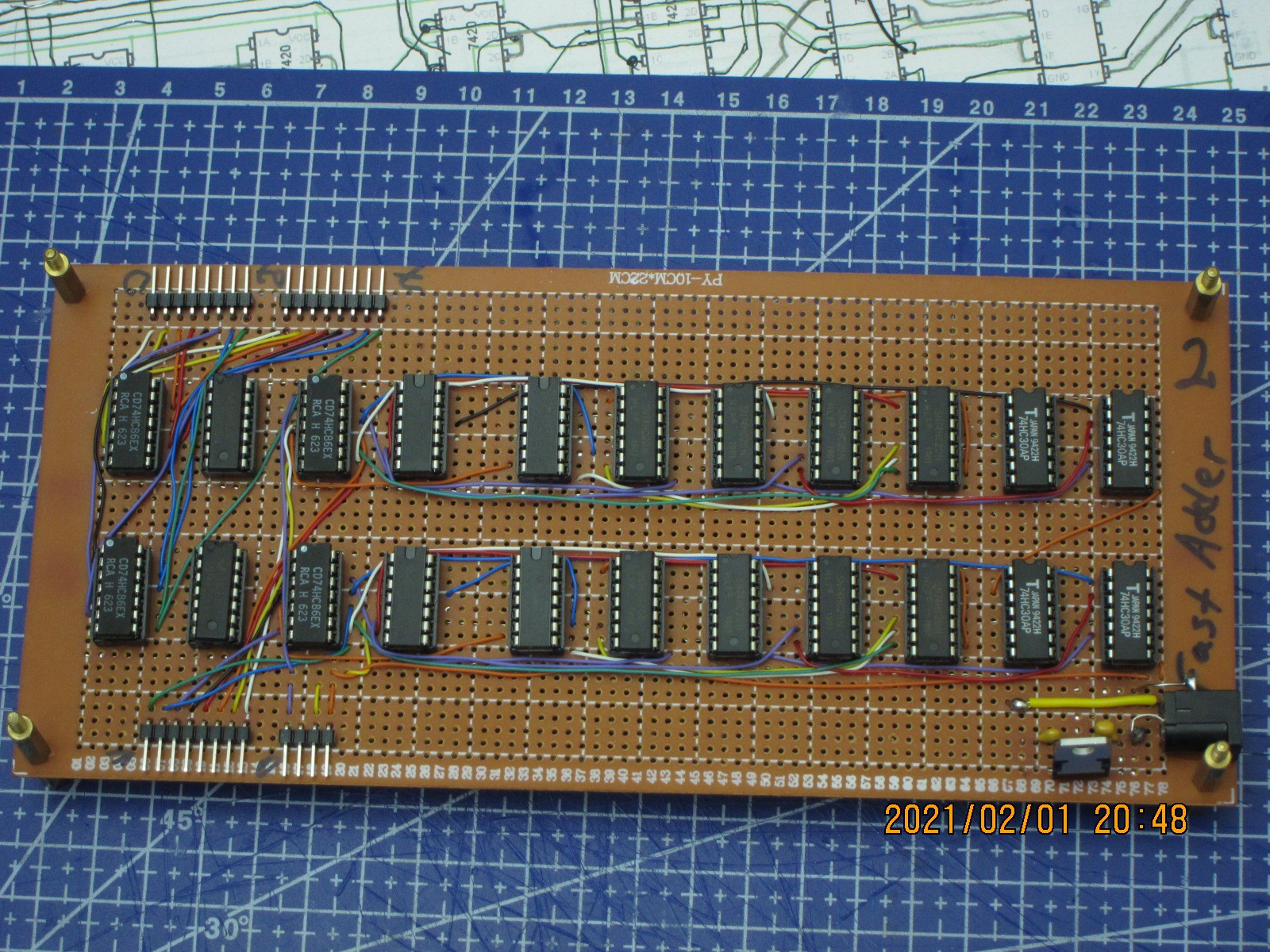
Two new 8-bit Fast Adder boards
02/01/2021 at 19:48 • 0 commentsI decided to start to really build the thing (at least ALU for a moment) -- with 16-bit adder as the first part of it. This adder is quite big and complicated, such that it takes up 2 big boards, each of which dedicated to adding a single byte. The adder requires 44 ttl chips to run, as this is a carry look-ahead one, and needs some additional logic when compared to the simplest ripple-carry adder.
I already soldered one such board, but it's quality has much to be desired, and I decided to make two new ones for the real deal.
Today the boards were finalized and checked using my handy control panel, and no defects were uncovered.
Following in plans is the soldering of logical operations board, which will provide 3 simultaneous 16-bit outputs: AND(A,B), OR(A,B), XOR(A,B). This board looks easier to solder than adders, as all connections are quite local. Basically it will have 4 identical groups of 4 chips, with no cross-connections.
More general plan:
1 - complete the ALU
2 - make a register file
3 - integrate RF with ALU, which will be the heart - the main datapath - of the whole machine, the place where number crunching is taking place. This part is planned really well as of now, and no changes will be done to it. The rest of the computer -- memory address circuits and controlling logic is still subject to change.
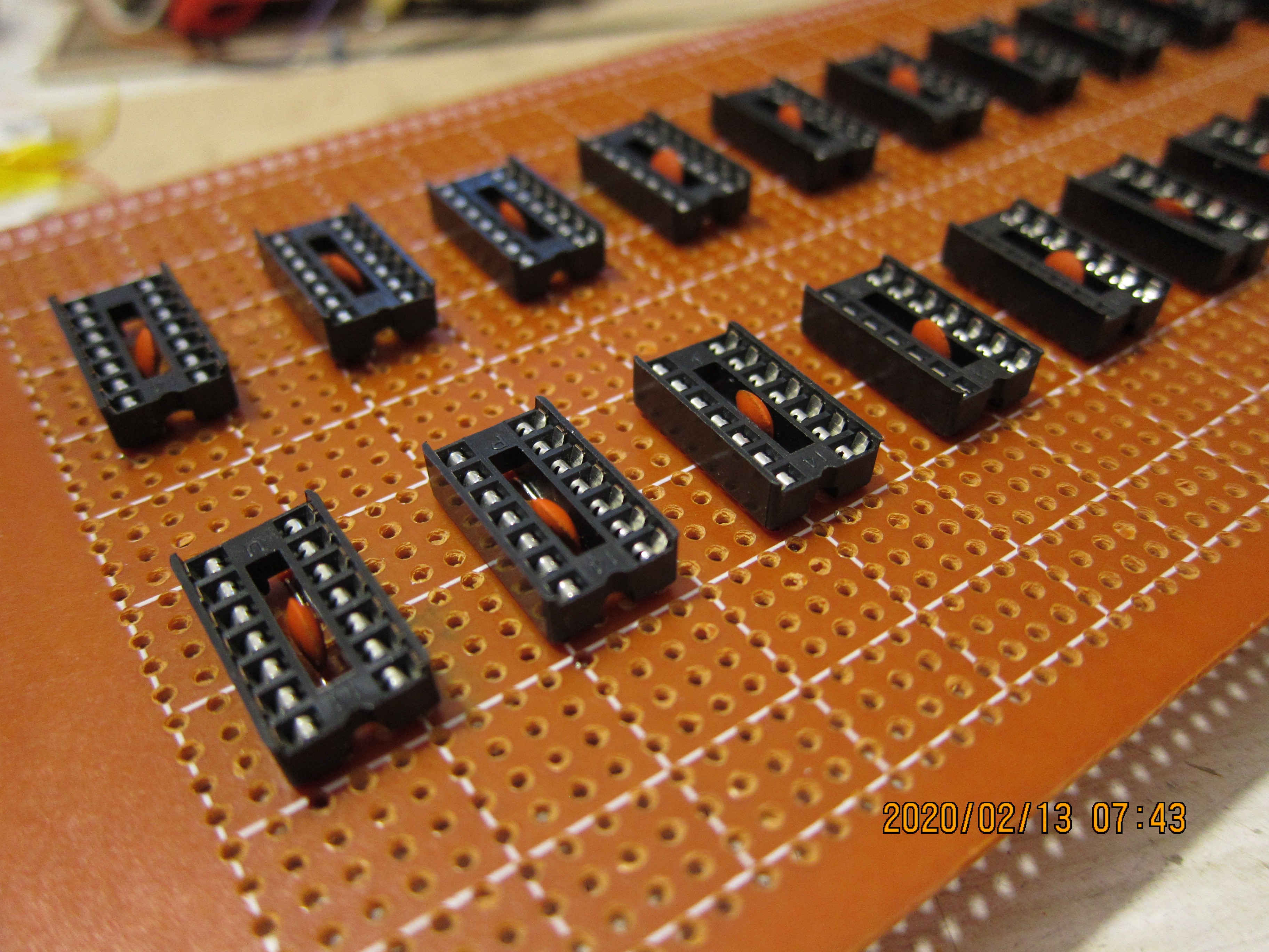
New boards:
1 - in the process of populating IC sockets with actual chips:
![]()
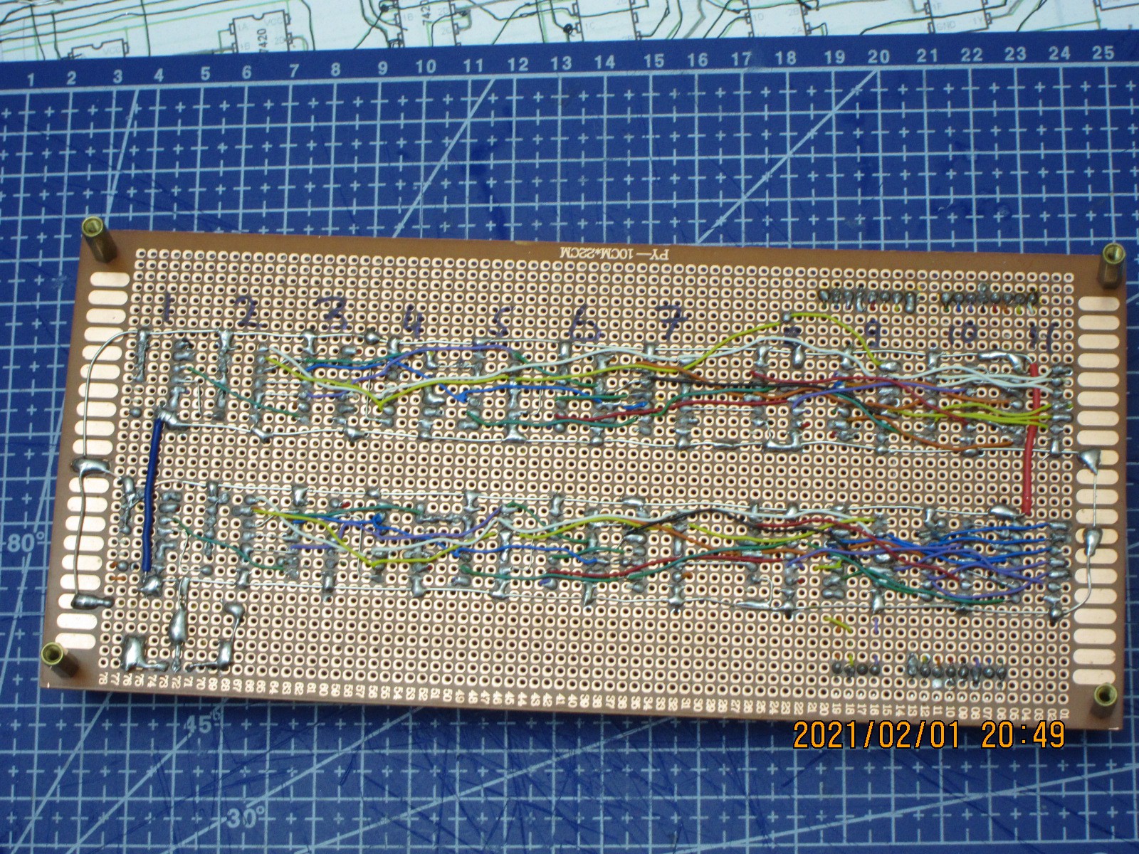
2 - Top and bottom sides of one of completed boards:
![]()
![]()
-
The first bit of actual hardware (Adder)
01/25/2021 at 09:58 • 0 commentsFirst, semi-experimental board with fast adders was completed at spring of 2020. It had a number of defects, and at the time I ran out of solder and as I was waiting for new batch to arrive from China, somehow I've lost interest in the project, so it was lying around just like that. This year, after some time playing with spectrometer project, I thought maybe revive this one, and took a hard look at the board, and debugged it; now it seems to be working good.
The defects were all due to the bad soldering, the wiring itself was fine. In several points solder joints were bad, as solder didn't made contact as needed. Also at some points these solder points broke after some time being okay, as the board itself was quite flexible, and the flexing of it led to joint breakage. To mitigate this in future, I glued plastic strips to the board to make it stiffer.
The board has mostly the same input/output interfaces as the 8-bit ripple adder made of discrete components (using diode-transistor logic), the control panel from that project is perfectly useful for testing this new one made of 74HCXX chips.
After successful debugging, I compared the speed of the new circuit to the old one, and results are quite fascinating:
The adders were setup to make the addition of carry_in to operands summing up to 0xFF, i.e.: 0x00 + 0xFF + C_in => C_out (0x1) + 0x00.
The carry in signal was fed from rectangular signal generator, which was also used as strobe signal for oscilloscope, and the carry out signal was measured by the same oscilloscope, thus the delay was measured.
For the DTL 8-bit ripple adder, the delay was near 30 microseconds, while for a pair of 4-bit fast adders with carry look-ahead, made of CMOS chips, the delay measured was tiny 120 nanoseconds, or almost 300 times less! Of course, this comparison is more like apples to oranges, but nevertheless, distinction between these two technologies is made very obvious by it.
Following are some photos of board building and testing:
1.1. basic layout (IC sockets only) - top:
![]()
1.2. basic layout - bottom:
![]()
2. Connecting the IC sockets in a way that makes the board a functional fast adder once proper chips are inserted into them:
![]()
3. Making the input-output interface for the board:
![]()
4. Testing the board using control panel from DTL adder project:
![]()
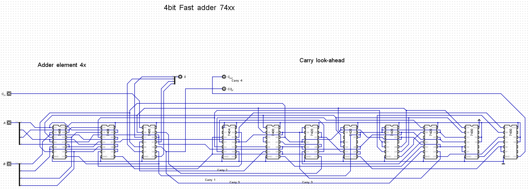
5. Schematic of the 4-bit fast adder, using chips, and optimised for minimum wire clutter and to be close to the way it is done on real board (the board itself holds two of these):
![]()
6. Schematics of parts of above circuit, done with individual gate symbols:
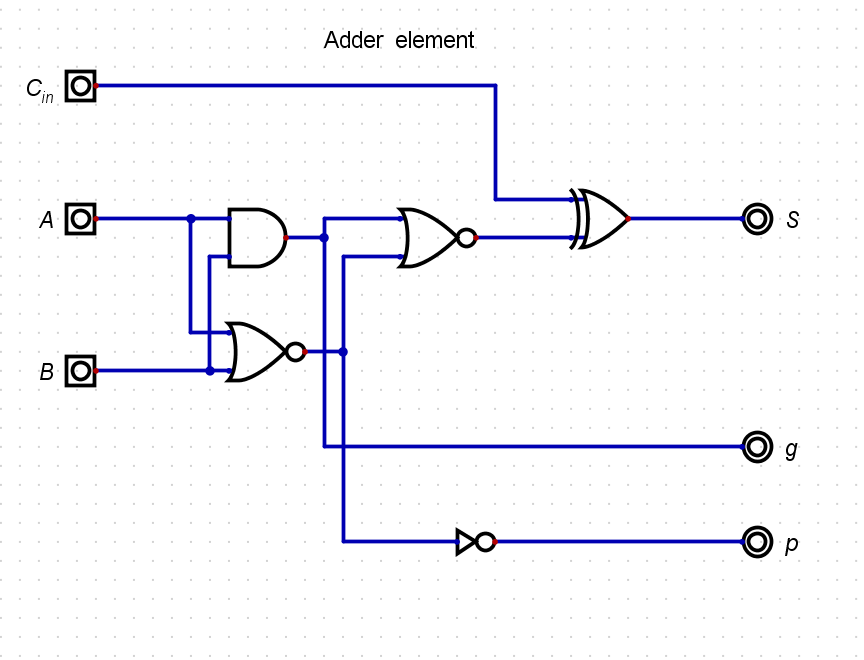
6.1. 1-bit Adder elements (4 of which are made with 4 leftmost ICs on the schematic above):
![]()
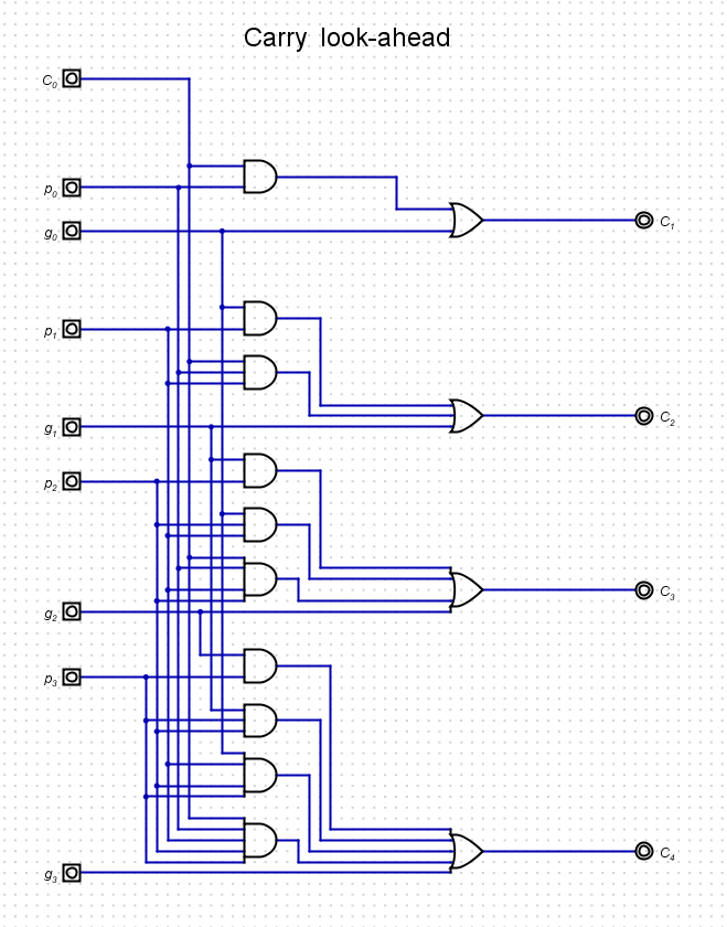
6.2. Carry look-ahead for 4-bit adder:
![]()
-
Thoughts on expanding addressing circuitry; Integer Calculator program
02/08/2020 at 17:56 • 0 commentsContinuing from previous post.
2020-02-06,07
It looks like I definitely need to add relative addressing mode. As I am reading K+R right now, I started wondering about how are "automatic" variables are created/implemented, and started searching info about it. This way I learned a lot about how stack operates, and about stack frames. This explanation is the best of all I've read.
It seems like having ability to push and pop one word at a time won't suffice for implementing proper function calls. (Well, there is still a way, but it is very awkward). So, I need to have the ability to access locations that are not only on the very top of stack, but a whole number of these locations (as many as needed for storing of all local variables and parameters for a given function. Having ability to access them by address which is known offset from known value (Stack Pointer or Frame Pointer) makes this much easier.
Thus it is now clear that addressing logic modification is needed, namely, adding an additional adder for calculating offset addresses. Now, as it became apparent that most of the circuitry will be muxes anyway, another adder now seems to be relatively small addition.
Given that there will be adder in addressing circuitry, then it seems logical to implement different additional addressing modes (various indexed ones). This of course would require yet another change to memory access decoding circuits.
These new modes should be mostly an addition to existing absolute addressing modes. One exception is that local (in-page) addressing will no longer be available -- this I already discarding with adding of byte addressing, as it adds much hassle for little gain.
Right now I could think of PC-relative and FP-relative (relative to Frame Pointer -- it is absent in simulation right now).
Also maybe GPR-relative mode also. The number of modes may be constrained by the number of available instruction bits.
Another implication of having an adder in addressing circuitry is that SP and PC are no longer need to be counters, but just a simple registers. On the other hand, after some thought, it looks like leaving these special registers the way they are now (counters which can auto-increment, and in case of SP, also auto-decrement) may serve a purpose - this way there is no need for dedicated hard-wired inputs of +2 and -2 for the address adder/subractor, so 2 inputs less to be multiplexed.
All of the above implies quite a bit of change have to be applied to the sumulation, as well as an assembler. As for the latter, I am already planning to rewrite it from scratch, in C rather than C++, in a way that will make it more plausible to write it in its own language eventually, i.e. make it native assemler, which will run on simulated (and hopefully physically built) computer, and produce code for that same computer. As of now it is of course a cross-assembler running on a PC.On topic of building hardware -- I've built a board recently, which may become, at least temporarily, a part of this machine -- the 256bit PROM (16 x 16bit words), made of switch banks, N4148 diodes and a handful of logic ICs. I gather, at the building and debugging phase it will be handier than burning EEPROM for each change. As a preliminary testing result, it seems like it can handle accesses at 1MHz, though I don't think such performance will ever be needed for a 32-byte PROM.
This board is described in more detail in my other project.--------------------------------
UPD 2022-11-07
Integer Calculator program
As of the start of the year 2020, I created assembly program for this version of ECM-16/ECM cpu, using the assembler I wrote earlier. This program is an integer calculator, i.e. it reads inputs as numbers and operators and returns the result.
For reading, it polls the Input register, and output is sent to segment digital display.
The calculator input and display are decimal integers.
After performing the operation, it halts, for the next operation reset is needed.
Here is screen capture showing how it works:
-
Adding byte addressing; and ramblings on some other topics
01/13/2020 at 06:36 • 0 comments2020-01-04: MemAccess wiring bug fixed: JSRg instruction now works
What to do with direct addressing modes?
There are two of them: local and global, local meaning only a page of 256 word is accessible, while global instructions can access any memory location, with a penalty of instruction being 2 words long and takes 1 clock cycle longer to execute.As jumps are used fairly frequently (in integer calculator they are encountered once per 5-10 instructions), leaving out the local instructions will bloat code 10 to 20%, and slow the execution by somewhere near 5% in terms of clock counts (this should be measured, for now it is a guess after looking at the code).
But these local jumps and load/stores are real pain in the ass when the program exceeds 256 words in length, because one should be careful that all of them are restricted to their local page and not try to reach adjacent one, as this will surely fail.
If to make a more sophisticated assembler, which will automatically check for this locality, and automatically choose global or local memory access/jump, this will make the assembly a highly iterative process -- as these kinds of instructions are differing in length, each change will affect all the addresses and alignment of the following code.PC-relative addressing -- not appealing.
Making these local references to be PC-relative rather than absolute will ameliorate the problem slightly, but this is not solving the issue with changing code length and jump/memory access lengths in the process of adjustment.Padding with "holes", with saving the page alignment -- this might actually be of some use.
Part of the solution would be to make holes in code, so parts which fit inside one page would have all internal references local, while references to other parts of program would be global. If the part of program is not taking up the full page, all the rest locations will be filled with zeros until the start of new page. Such padding would be quite a waste of memory space, but will offer slightly faster execution without complications caused by shifting code across page boundaries.--------------------------------------------------------
2020-01-05
Thoughts on byte addressingThis starts to seem inevitable that byte addressing should be added. This will ask for hardware update, so special instructions for byte loads and stores could be done (memory addressing circuitry mainly, but also changes to memaccess decoder), as well as update to the assembler.
Right now the machine is happily working in word addressing mode, but this seem only good for number crunching; while working with characters had not yet been explored. This now seem that it could bite me in the ass in the future.
--------------------------------------------------------
2020-01-12
Byte addressing is implemented.
Simulation now in its version 5.0
Version incremented due to addition of new functionality -- namely, byte addressing.
Comment by Ken Yap regarding lack of byte addressing provoked thoughts on this topic. Although in my reply I wrote that this seems to be of no big consequence, afterwards I started to think about this deeper. So far I am implementing a calculator program, and it cannot care less if byte addressing is present or not, as it works with words. But to make programming for other problems easier on this computer, adding byte addressing seemed better and better idea. There are thoughts of implementing C compiler for it in some distant future, and it is the kind of thing which would benefit from ability to address individual bytes.
So, as of right now, I implemented it. On one hand, this was not as difficult as I thought it would be. On the other hand, some sacrifices were made (not that these were real): total addressable memory has been reduced at least 4 times: first, halved because now addressable unit is 8-bit byte instead of 16-bit machine word; second, I need additional bit in instruction word for loads and stores to indicate that I want load or store individual byte (and there were no available bits in high half of instruction). So, instead of possible 16MWords (32MB) I now can only address 8MB of memory directly. On the other hand, at least for now, I don't think there will be need for more. But if such need arise, in some far future time, the solution will be found. Right now my calculator program is just over 1kB in size.
Addition of byte addressing, and particularly, of the ability to manipulate individual bytes, have lead to thoughts in other direction: maybe add ability to load/store and push/pop multiple words in one instruction? Especially push/pop entire register file, all 8 registers in one instruction. This will be neat capability, when used in conjunction with subroutine jumps and interrupt service routines.For this implementation following changes were made:
Computer simulation:
As Program Counter and Stack Pointer are implemented as actual counters, to make them increment by two instead of one, bus was shifted on them, so the least significant bit bypasses the counters and is not affected by counting. This least significant bit of address is ignored on most instructions except in byte loads and stores.
The memory subsystem was redone as 8-bit units. The ROM is 8-bit, and RAM is two 8-bit elements. Circuitry for optional single byte selection was added.
Memory access operation decoder was augmented slightly to accommodate single-byte loads and stores. Now, single-byte directly addressable stores and loads are possible, as well as byte stores/loads using register and register-memory indirect modes.Assembler: the addresses now calculated taking into account that individual bytes are counted. The output now produces a column of 2-digit hex numbers, instead of 4-digit ones, so as to fit in ROM with 8-bit data output.
The simulation, version 5 is added to files.