-
Timing considerations
01/02/2022 at 03:46 • 0 commentsJOYMEGA MODE
During the execution of the JOYLIB.GTJOYMEG6 from HIDLIB, the Z80 calls a function to read the Joystick right after it flips the state of the Pulse pin ..
...
    call    BASELIB.FLIPPORTOUT    ;
    call    BASELIB.RDJOYPORT;
..
Tracing the assembly instructions the time it takes from the pin change (OUT instruction) to the reading (IN) is 100 cycles (see below) or ~28us.
In terms of AVR cycles it means 100 * (8MHz/3.58MHz) or 223 cycles to spend with latency. After discounting 11 cycles for the latency of a pin change interrupt theres is still more than enough processing time for not to worry with the compiler overhead.
call    BASELIB.FLIPPORTOUT
    BASELIB.FLIPPORTOUT:
    ld    a,e
    xor    d        ; flip Output
    ld    e,a
    ld    a,15
    jp    WRTPSG

    WRTPSG:
    DI
    OUT    (PSG.LW),A    ;LATCH ADDRESS
    PUSH    AF
    LD    A,E
    OUT    (PSG.DW),A    ;OUTPUT DATA  ; 12
    EI                                 ; 5
    POP    AF                          ; 11
    RET                                ; 11


call    BASELIB.RDJOYPORT              ; 18
    BASELIB.RDJOYPORT:
    ld    a,14                         ; 8
    di                                 ; 5
    call    RDPSG                      ; 18
    RDPSG:
    OUT    (PSG.LW),A                  ; 12
    IN    A,(PSG.DR)
    RET
    ei
    ret
; 12+5+11+11+18+8+5+18+12 = 100
BASIC MODE
The timing on Basic mode is a bit shorter, 60 cycles from the instruction that rise the level of the Pulse pin until the first reading on the joystick port.
It is still enough time to deal with the code produced by the compiler as it represents ~17us or 134 AVR cycles (at 8MHz).
GTPDL: INC A ;Force parameter 2 based AND A RRA PUSH AF ;Save port # (carry reset if port 1) LD B,A XOR A SCF PDL1: RLA ;Form mask pattern DJNZ PDL1 LD B,A ;Set mask pattern POP AF LD C,10H ;Assume port 1 LD DE,03AFH JR NC,PDLP1 ;Good assumption LD C,' ' LD DE,4C9FH PDLP1: LD A,PSG.PB DI CALL RDPSG ;Get current port B content AND E OR D OR C OUT (PSG.DW),A ;Set trigger high ; 12 XOR C ; 8 OUT (PSG.DW),A ;Set trigger low again ; 12 LD A,0EH ; 8 OUT (PSG.LW),A ; 12 LD C,0 ;Initialize counter ; 8 PDL2: ; total: 12+8+12+8+12+8 = 60 IN A,(PSG.DR) ; 16.76us / 134 AVR cycles @ 8.0 MHz AND B ;End of pulse? JR Z,PDL3 ;Yes INC C ;Bump counter JP NZ,PDL2 ;No overflow yet DEC C ;Make it 255 PDL3: EI LD A,C ;Return counted value RET -
Development environment (updated)
07/27/2020 at 03:32 • 0 commentsMost of the logic have been tested using Arduino sketches and debugged on the serial terminal. It might have been done with a C compiler and a debugger but using real hardware allowed me use real controllers.
Next step involves timing and interrupts, as well as a connection to the MSX.
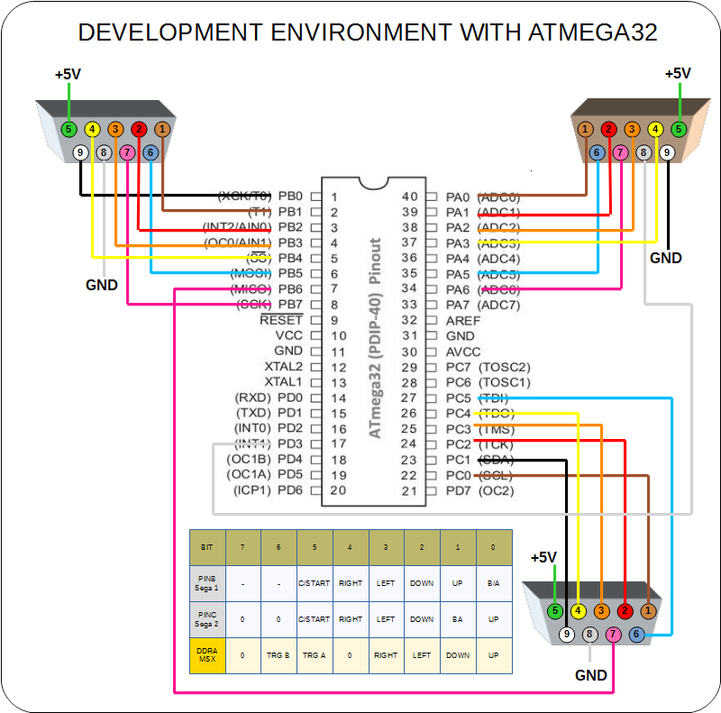
Since the circuit uses the internal oscillator and the crystal pins as I/O it is advisable to make the development using another environment: a bigger AVR (in the sense that it provides more pins). The chosen one was the ATMega32 that I have lying around on my parts bin. A rough drawing of the schematics is shown below. The output to MSX is done with PORT A leaving PORT D for loading and debugging.
A slight difference is that external interrupt 1 was used because ATMega 32 does not have pin change interrupt capability.
![]()
-
Making a 6 button loke like a 3 button or SMS controller
07/26/2020 at 18:37 • 0 commentsThe function scanControllers( ) can detect if the controller is a 3 button or a 6 button or even a Master System SMS controller and return a 16 bit value with the following format:
// 15 14 13 12 11 10 9  8  7  6  5  4  3  2  1  0
// 0  0  0  0  MD X  Y  Z  ST A  C  B  RG LF DW UP
I have some 6 button controllers but none with 3 button neither a SMS controller, but if the pin SELECT is tied to a fixed logic state then the controller will change its behaviour, being detected as:// SELECT = HIGH: SMS controller // 15 14 13 12 11 10 9 8 7 6 5 4 3 2 1 0 // 0 0 0 0 0 0 0 0 0 0 C B 1 1 DW UP// SELECT = LOW : 3 Button controller // 15 14 13 12 11 10 9 8 7 6 5 4 3 2 1 0 // 0 0 0 0 0 0 0 0 0 0 ST A 1 1 DW UPNotice that 3 button controller will show LEFT an RIGHT both pressed and START and A instead of B and C, nevertheless the controller is being detected as a 3 button.
-
PCB ready!
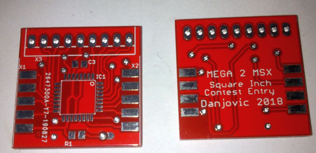
10/10/2019 at 03:19 • 0 commentsPCBs just arrived. Routing was done in 2018 but I have just ordered the boards last month.
![]()
-
Expanding: Reading all buttons
09/19/2018 at 02:23 • 0 commentsIt is possible to expand the functionality of the adapter using the same technique as the Megadrive to read the 6 button joystick.In normal operation the selection between Controller A and Controller B is performed by changing Pin 8 from MSX joystick port, then reading the state of the buttons.
As the signal from MSX pin 8 can be stuck at any value it is necessary to poll the Megadrive controllers and constantly update the state of the pins at MSX joystick port and such task is performed once at each 16.384ms.
Once an interrupt occur by a change in pin 8 the state of the pins at MSX joystick port is updated and the next poll is programmed to occur 16.384ms after the end of interrupt routine.
Expanded mode allows the reading of all buttons from a 6 button Megadrive controller and can be accessed after issuing 4 consecutive rising edges on pin 8 from MSX port within one poll cycle interval. The state of the pins will be then determined both by the state of pin 8 - denominated PHASE - that can be Low or High, and by the bit 0 of a rising edge counter that might be either even or odd.
-------MSX PIN STATE-------------
8        1   2   3   4   6    7
Low      UP  DW  LF  RG  BtA  BtB (Contr. A)
High     UP  DW  LF  RG  BtA  BtB (Contr. B) 1st pulse
Low      UP  DW  LF  RG  BtA  BtB (Contr. A)
High     UP  DW  LF  RG  BtA  BtB (Contr. B) 2nd pulse
Low      UP  DW  LF  RG  BtA  BtB (Contr. A)
High     UP  DW  LF  RG  BtA  BtB (Contr. B) 3rd pulse
Low      UP  DW  LF  RG  BtA  BtB (Contr. A)
High     UP  DW  LF  RG  BtA  BtB (Contr. B) 4th pulse
Low      UP  DW  LF  RG  BtA  BtB (Contr. A)
High     UP  DW  LF  RG  B    C   (Contr. B - Raw ) 5th pulse
Low      UP  DW  LF  RG  B    C   (Contr. A - Raw )
High     Z   Y   X   MD  A    ST  (Contr. B - Raw ) 6th pulse
Low      Z   Y   X   MD  A    ST  (Contr. A - Raw )

High     UP  DW  LF  RG  B    C   (Contr. B - Raw ) 7th pulse
Low      UP  DW  LF  RG  B    C   (Contr. A - Raw )
High     Z   Y   X   MD  A    ST  (Contr. B - Raw ) 8th pulse
Low      Z   Y   X   MD  A    ST  (Contr. A - Raw )

...
...
...
Expanded mode is exited by timeout after the next polling cycle
-
Safeguard
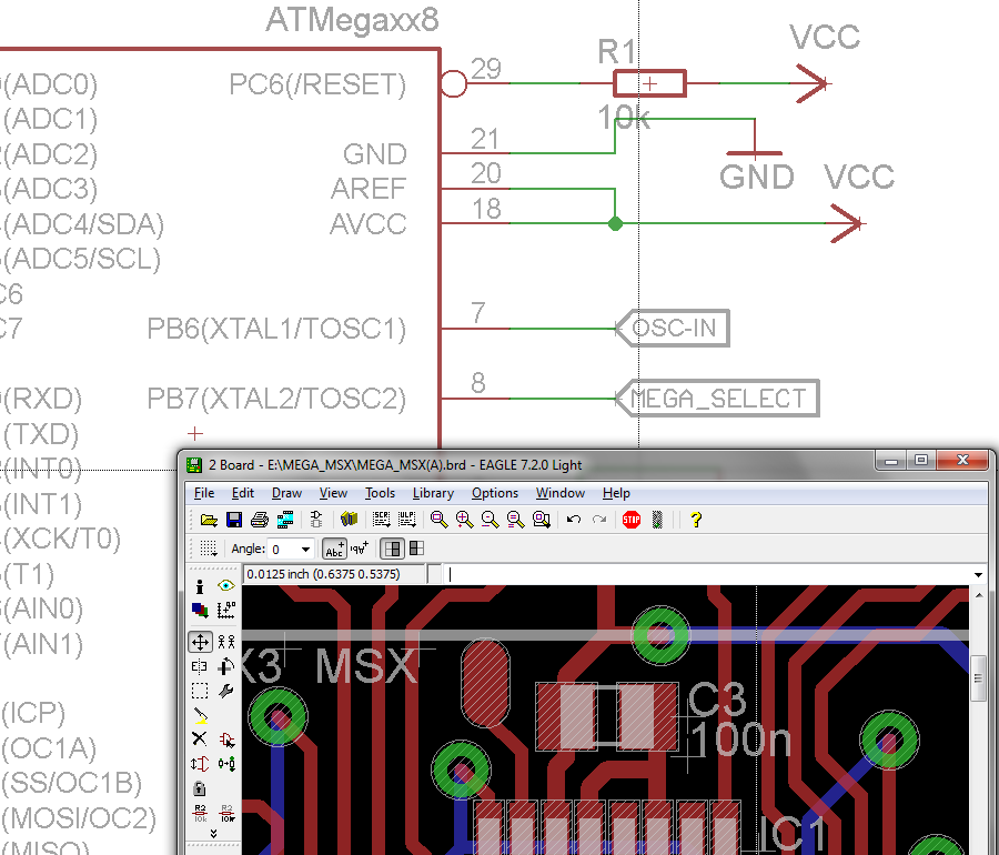
09/18/2018 at 23:41 • 0 commentsAs this project uses internal clock I have merged both SELECT inputs from Megadrive cotrollers in a single line at pin PB7 OSC-OUT and left pint PB6 OSC-IN open just in case something go wrong with the fuses configuration and the AVR would expect to operate from external crystal.
A track was added to pin 7 which ends in a large track. Over the latter another track on the TSTOP layer as added so the solder mask will not be poured over it
![]()
-
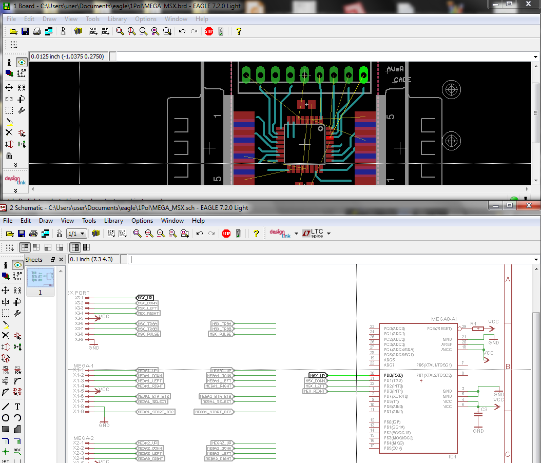
Iterative design
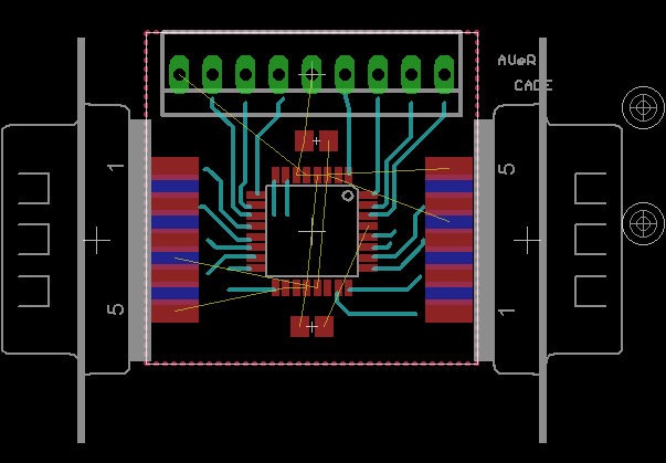
08/23/2018 at 02:05 • 0 commentsSuch small boards require some iteration in design:
- Lay the components,
- Choose the pins to use for each function
- Draw some straight lines between pins that shall be interconnected
- Connect pins schematic
- Route the board
- Repeat all steps as necessary until routing is finished (and you're happy with it)
![]()
![]()
 danjovic