-
Boson 640 working.
10/01/2018 at 06:46 • 2 commentsAfter working on updating the verilog module used in my camera to support the HyperRAM using DDR modules and the PLL of the ECP5 FPGA I'm using.
The change increased the performance by 4x. This enables us to capture the datarate from the Boson 640 cores.
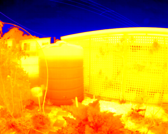
Here is a photo of the water tank ~80% full.

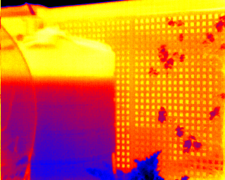
For reference here is the same tank using the Boson 320 core.

There are still many performance improvements I have on a list to work on.
But the major functionality of the device is working. We can capture Images at about 3 FPS.
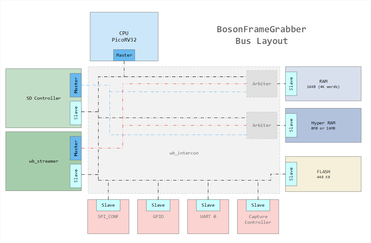
Here is the layout of the internal modules in the FPGA All the components make use of a common wishbone bus. There are 3 masters that enable data-flow through the device without requiring the CPU. Basically these are simple DMA controllers.
Everything is wired together using wb_intercon (https://github.com/olofk/wb_intercon). This package automatically creates a verilog file with muxes/arbiters/address decoders based on a simple config file.
I'm using picoRV32, as this worked very well on the HX8K hardware I started with. I studied RISCV in a computer architecture class, so I have a good base of knowledge when debugging issues. The CPU handles the filesystem using FatFS. This enables us to access FAT, and exFAT formatted SD cards.
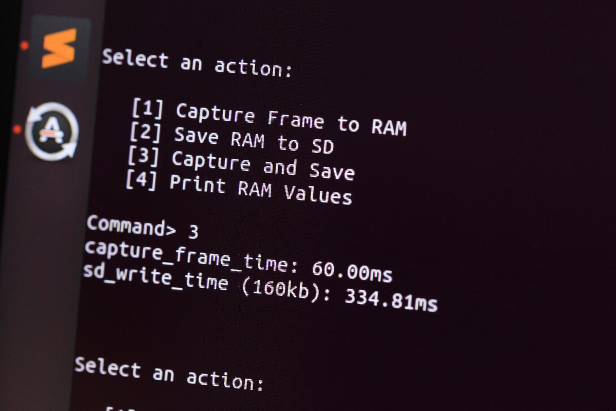
The firmware is still very basic. It's operation is as follows- Prime wb_streamer to capture the camera stream into HyperRAM.
- Wait for vsync signal from the camera.
- Capture 1 frames worth of data.
- The RISCV handles creating and allocating a new file. (IMG_0001.RAW)
- The DMA of the SD controller writes the file contents from HyperRAM into the SD card.
- We Finally blinks a LED and repeat.
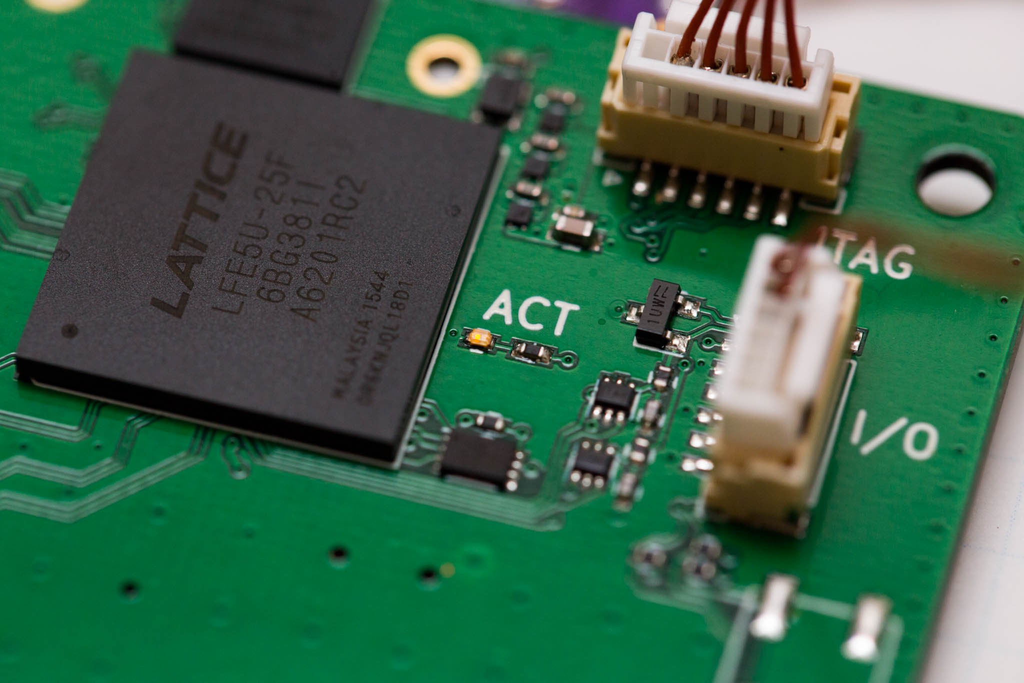
To the user once powered all they see is the LED on the back of the camera blinking away. -
SD optimisations
10/01/2018 at 06:29 • 0 commentsWhen working with low level SD drivers, there are few things you need to do in order to get anywhere near the actual write speeds advertised on cards.
MULTIPLE_BLOCK_WRITE (CMD25) is probably the most important things you can do. This needs to be combined with SET_BLOCKLEN (CMD23) in order to tell the internal logic in the SD card about our intention to write more than 1 block.
Here is an example of writing a 512kb file to an SD card. (1 bit mode, 12MHz clock, exFAT FS)

About 2.5s, this results in a write speed ~204kBytes/s. When running in 1bit at 12MHz our bus speed is ~1500kBytes/s. Even with overhead of filesystems we should be able to do better.Lets switch to using CMD23 and CM25.

For clarity the scale remains to same. This time it took 0.45s, which results in ~1100kByte/s write speed. MUCH better!
You will notice that the CMD line is active during the transaction, this indicates a start/stop of dataflow. Why? This is due to the structure of the file system. By default FatFs will only write continuous streams until you hit a cluster boundary. In this case this card was formatted with a 32kb clusters. this results in 16 separate transactions.
Every one of these transactions incurs a 1ms write time when the card is busy, and can't be used. FatFs includes a command that lets you pre-allocate continuous space for a file. f_expand. If we use f_expand then we can perform all our filesystem tasks in one go. then have a free-run to write the file out.

Total time 0.42 = 1200kBytes/s
We are still operating in 1bit mode, 12MHz. All we have done is alter the firmware. I'm using high quality Samsung cards that have a stated max write speed of 60MB/s. You can see that we don't incur any delays while writing all the main data for the file.
In order to reach a 60MB/s write speed you require hardware that can switch the signalling to the SD card into UHS mode. This uses 1.8V signaling, instead of the standard 3.3V.
As my hardware does not contain this additional hardware, so I'm limited to using HS mode. 50MHz 4bit which should enable near to 25MByte/s.
-
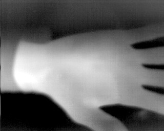
First Image captured!
09/27/2018 at 00:45 • 0 commentsAfter spending a few weeks tracking down a bug caused by a bad reset circuit and incorrect PLL usage. I've finally captured an image using the new hardware!

It appears that I've lost the first pixel in the frame somewhere into the ether. This results in the single pixel band down the left side of the image.
Still some more work to do in terms of performance. Almost every part of the design can be improved in same way to improve the speed at which I can record these images from the camera module to the SD card.
- SD multiblock write
- SD 4bit mode
- Burst read from HyperRAM -> SD controller
- Use PLL for HyperRAM (4x speed increase)
- Set HyperRAM latency to lowest speed + variable latency (~2x speed increase)
- FatFS f_expand() + single low-level multblock write
The next stage in the project is working on the SD low level drivers to support CMD25 (Multiple block write). When combined with CMD23/ACMD23 (Number of blocks to erase) we can really boost the write speed of the SD card. At this time the image is written in 512 byte blocks to the card, the card accepts this block and performs an erase/write on its internal FLASH. I'm using high quality Samsung cards, and I see this process takes ~1ms
You can see the start of the image being written to the card. The first reads/writes are dealing with the exFAT filesystem, the regular pattern on the right side is the image data written in 512byte blocks, and subsequent busy cycle from the card. The SD card indicates it is busy by holding the DAT line LOW.
You can see that our data cycle and busy cycle are pretty even right now. Data cycle takes ~0.7ms, busy: ~1ms. If we enable 4bit mode now we can decrease the data cycle by 4, but the busy cycle remains unchanged. This results in very little overall speed improvement.
-
Not another PCB.
09/09/2018 at 07:09 • 0 commentsThe thought of shelving this project for 8 weeks waiting for the FPGA left me discouraged. What if after 8 weeks I assemble the board and it doesn't work?
I decided to create a new PCB, this time using an ECP5 in a larger 381 ball (17x17) package.
 ---------- more ----------
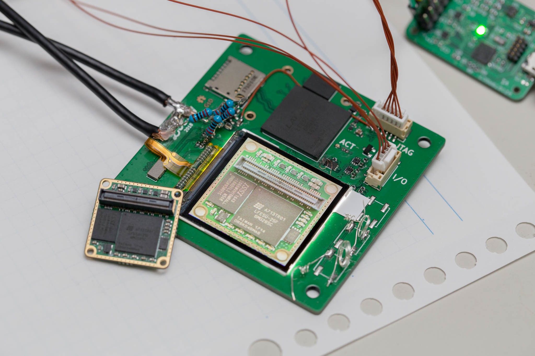
What started as a reasonably small board, soon ballooned as I decide to add an LCD screen. (Why not?)

Unfortunately in the rush to get this board made (I designed it over a weekend) I had introduced a few errors.
- Config flash was not wired up correctly. The ECP5 supports many different configuration methods, and I was not clear in my naming of the signals required in the schematic.
- I had shorted out an internal power rail by adding the via stitching and not running DRC before ordering (rookie mistake) These were fixed by simply drilling out the vias.
- The backlight DCDC circuit for the LCD wasn't connected to a power rail.
- I had incorrectly set the configuration strap pins. so the FPGA would never attempt to load a config bitstream from external flash.
But the good news, I did not make any of these errors on the small boards I already had manufactured. these were all introduced when I swapped my schematic symbols from the 285 pin device to the 381 pin one.
Since I had correctly connected the JTAG pins I was able to program the FPGA after it was powered. So that's something....

I even did some green-wire fixes to support the FLASH IC. I'm programming the FLASH though the ECP5 in what they call "Background SPI programming". This works great, but does require the FLASH chip be connected to the correct pins on the chip.

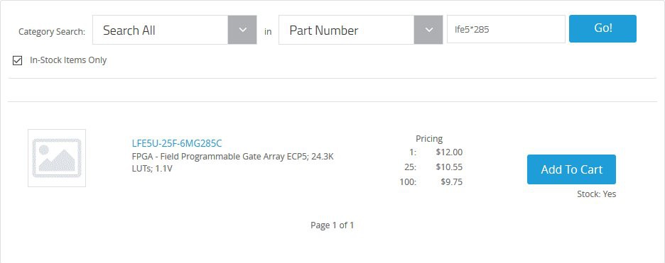
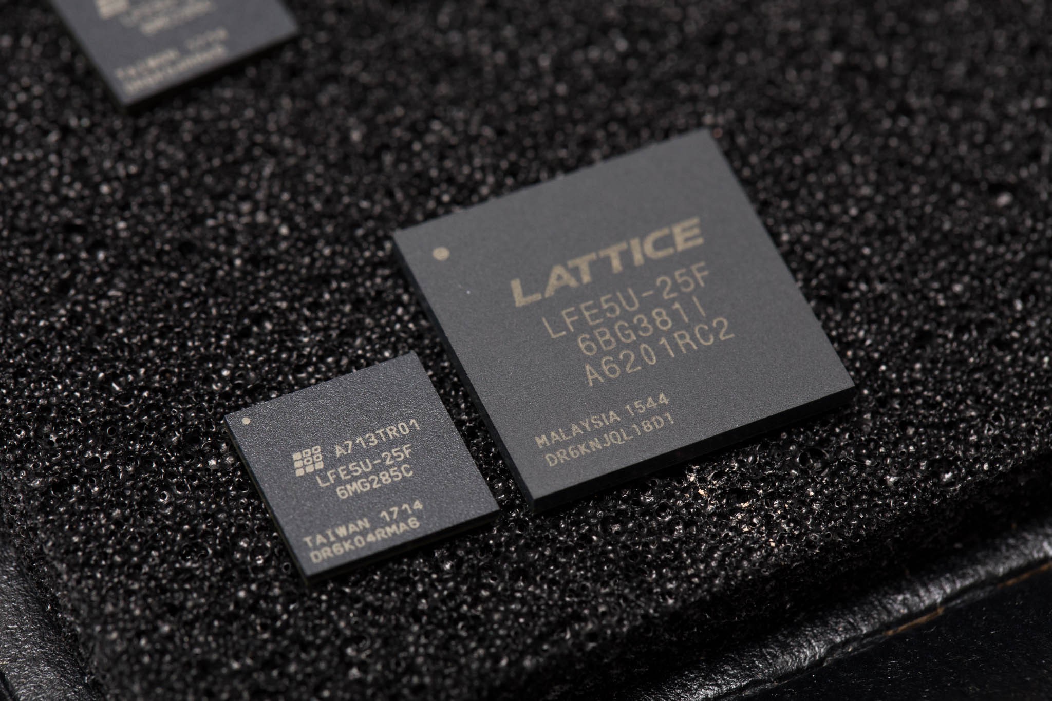
While working on this board did keep me busy for 2 weeks, it was all for moot. I'd been checking the lattice webstore for ECP5 stock every couple of days. The day after assembling this larger test board I find they have stock of one product line in the 285 ball package.

Lattice actually uses Mouser as their fulfillment center for their webstore. So I checked Mouser, and yes they had a tray of the FPGAs in stock. I bought a few as spares.

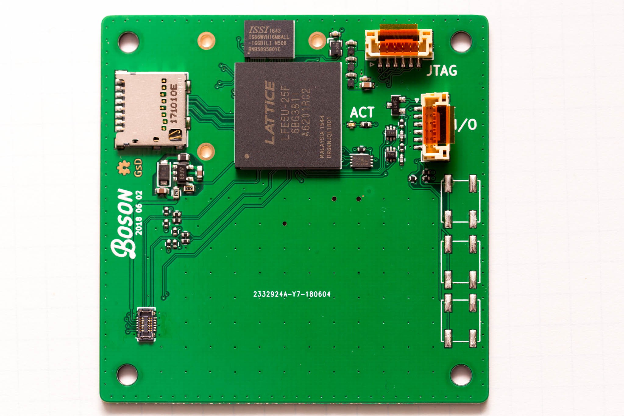
With these FPGAs in my hands I assembled up my first v1_02 PCB. Even though the spacing between parts is very tight, it's actually not too difficult to assemble one of these boards by hand under a microscope. I'm using lead free solderpaste and a stencil (from OSHStencils). The boards are double sided. The reverse side I currently hand-solder. You do have to be careful about the order in which you solder parts as to leave clearance for the iron.

I did end up playing around with that LCD I'd put on the big-board. It's an ipod nano 240x240 IPS panel. Mike Harrison did a great job reverse engineering it (http://www.electricstuff.co.uk/nanohack.html) Following his instructions I manged to replicate the MIPI bus using the ECP5. I even had to make up some x10 low impedance scope probes, which he explains in his very detailed videos. I might revisit the big-board and a project with the ECP5 and an LCD screen at a latter date.
 -
Performance, a new camera, another revision?
09/09/2018 at 06:36 • 0 commentsWith v1_01 working. I now had a better understanding of working with verilog, and a much better understanding of LUT utilization and timing closure. I'd managed to fit in a hardware SPI module, with DMA. with these improvement and the system running at 24MHz (max frequency of my design typically sat around 30MHz for the iCE40HX) the 160Kb images from the camera took around 300ms to capture. Not bad!

But the iCE40HX8K, while a great little chip is too small and under powered to really push this project to the next level. I had designed the PCB to accommodate a 4bit SD interface, I had wired CMD,DAT0-3,CLK to the FPGA. Using SPI mode was easy to validate that the hardware was working. But for a notable performance increase I'd need to switch to a real SD controller. The controller I wanted to work with (https://github.com/mczerski/SD-card-controller) did not fit in the remaining space of the iCE40HX8K.
Around this time I was contacted by GroupGets. a distributor of the FLIR Boson. They were very impressed with the work I was sharing on twitter, and donated a Boson 640 for me to test with and ensure everything worked.

This Boson 640 is a beast! 640x512 pixel resolution, 60Hz update rate, and this has the widest angle lens: 95 degree FOV.
Unfortunately the added pixels (4x an many!) and the added frame rate means this camera uses a 27MHz pixel clock. This did not play well with my 24MHz capture hardware. I needed to rebuild it. Better, faster....(stronger?)
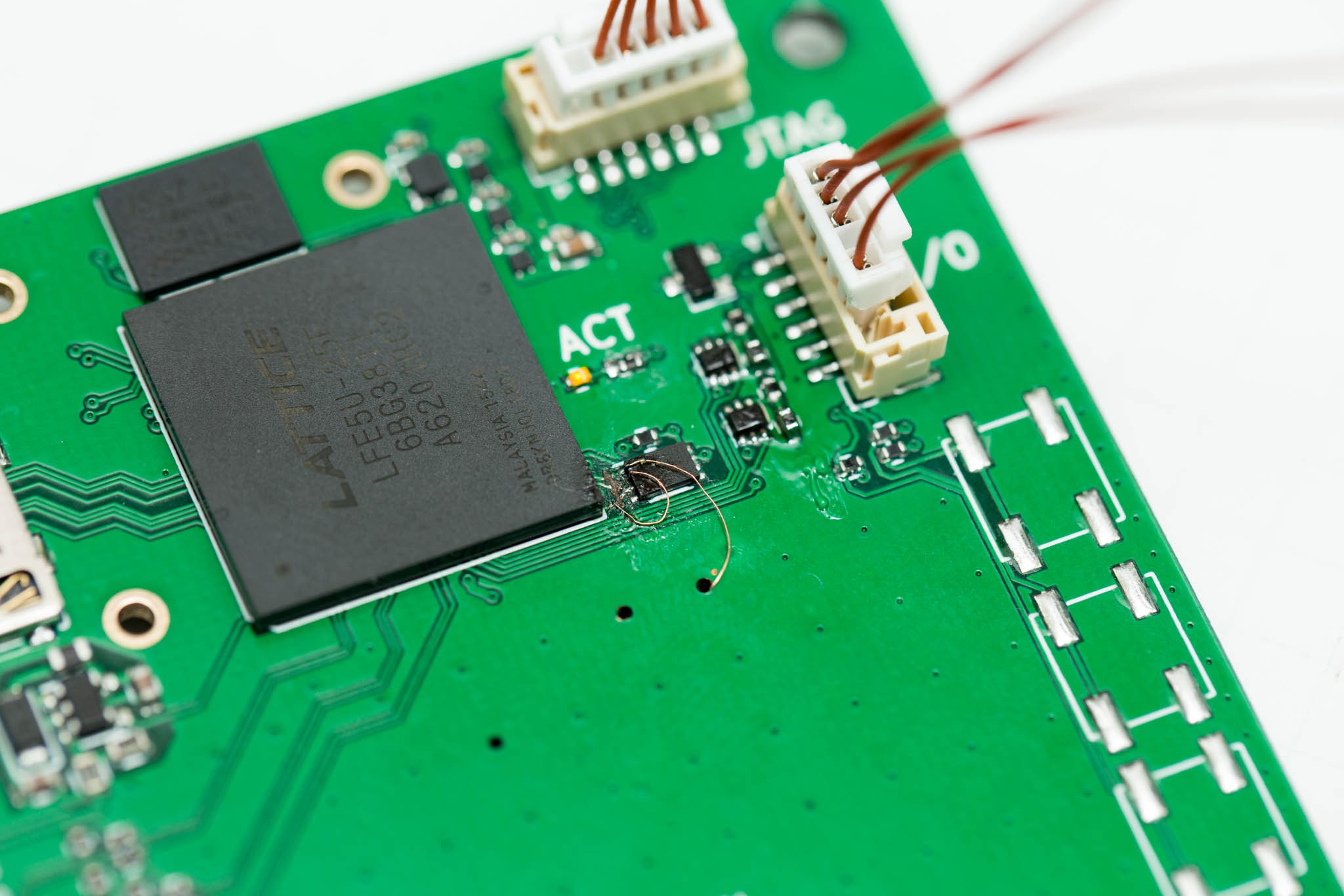
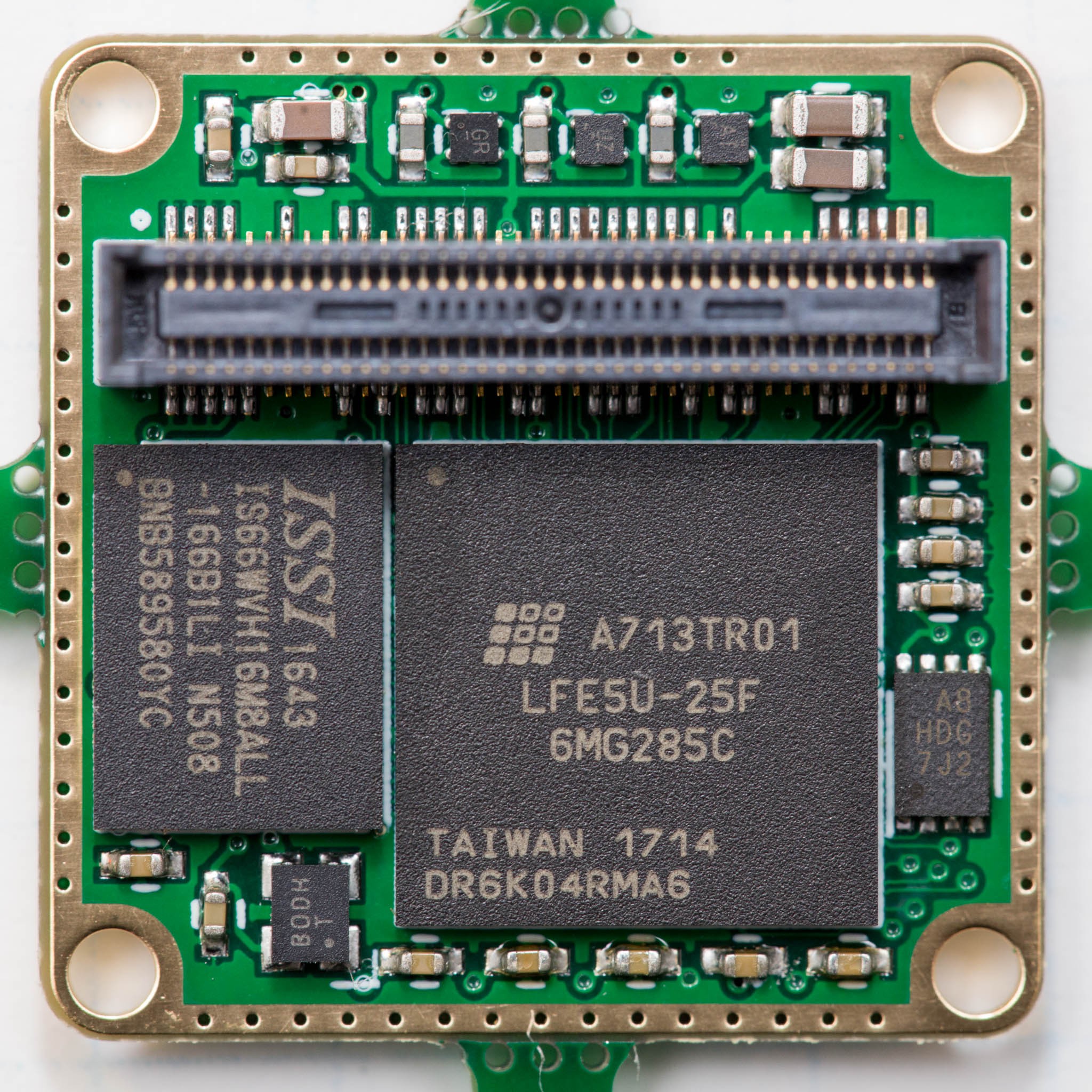
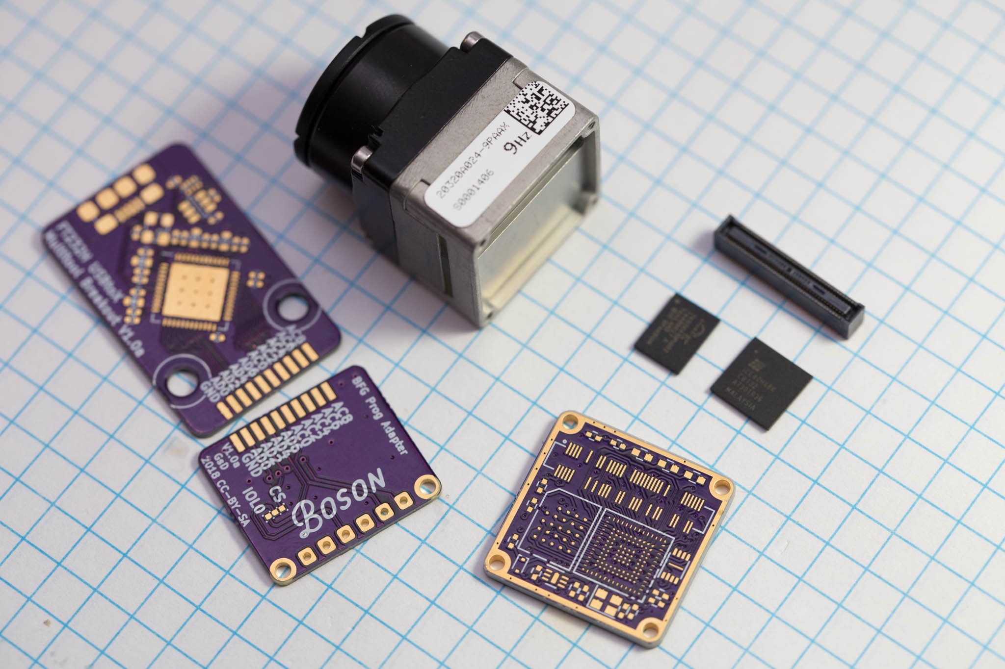
---------- more ----------Replacing the HX8k was not easy. Most FPGAs are in huge BGA packages, the ones in small packages typically only have a handful of logic for simple glue logic in modern portable tech. I was very comfortable with Lattice at this point, and finally found the ECP5 line had a 10x10mm package version. While a bit bigger than the HX8K's 8x8mm it might just fit. So I created a footprint and added to my board in KiCad.

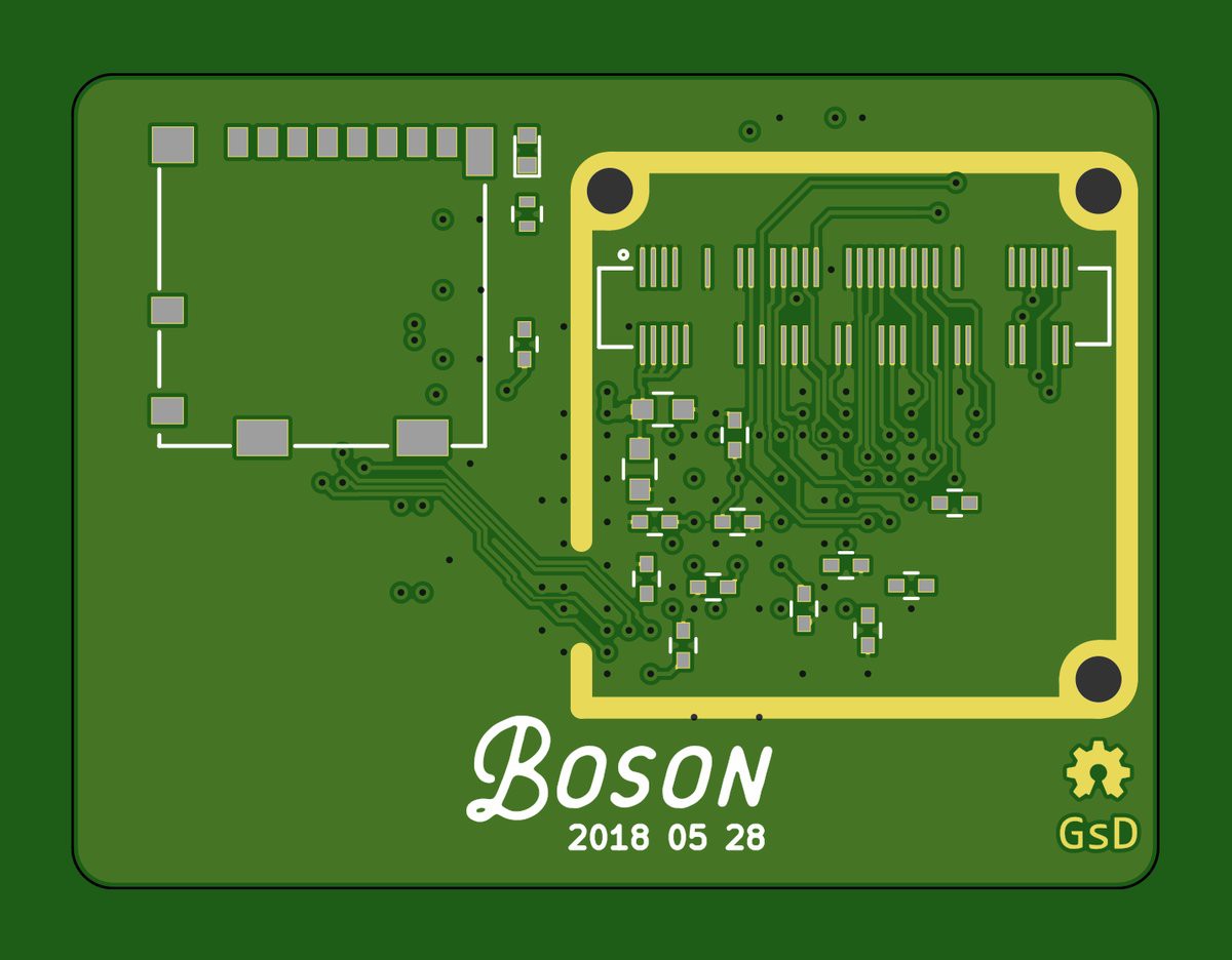
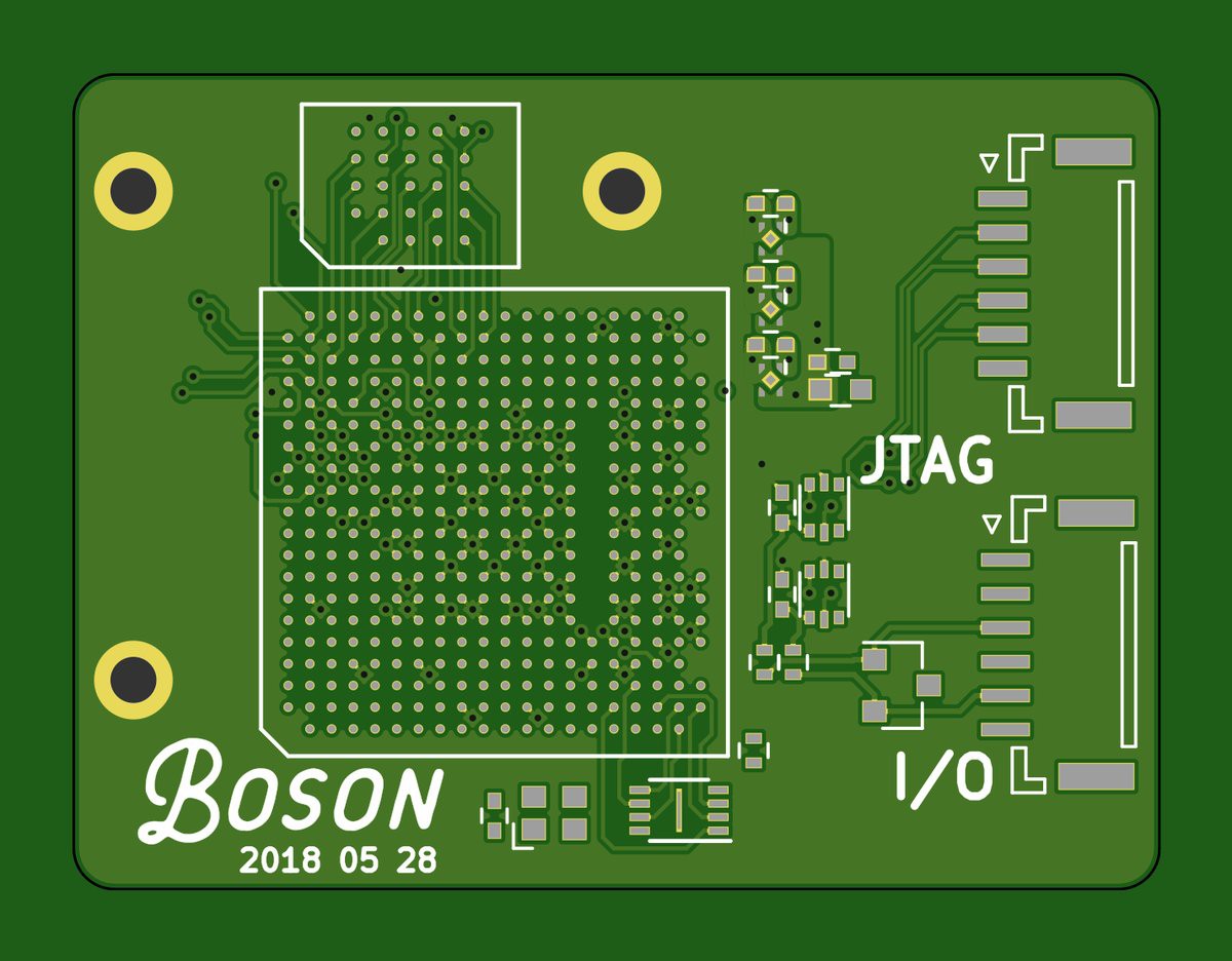
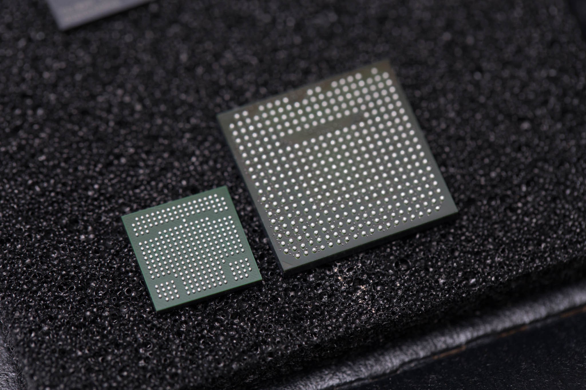
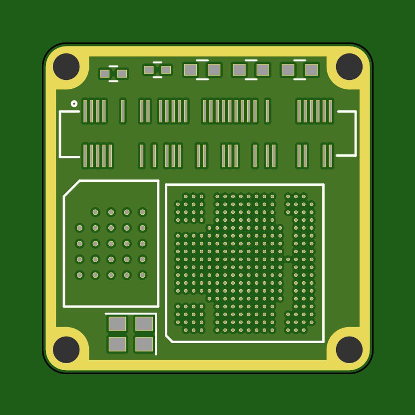
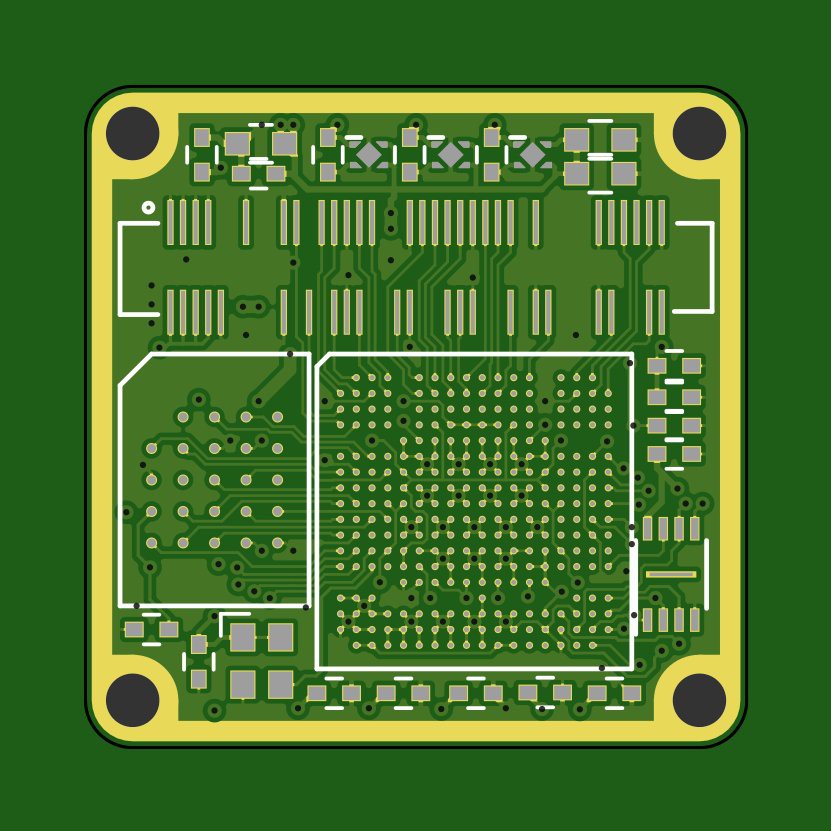
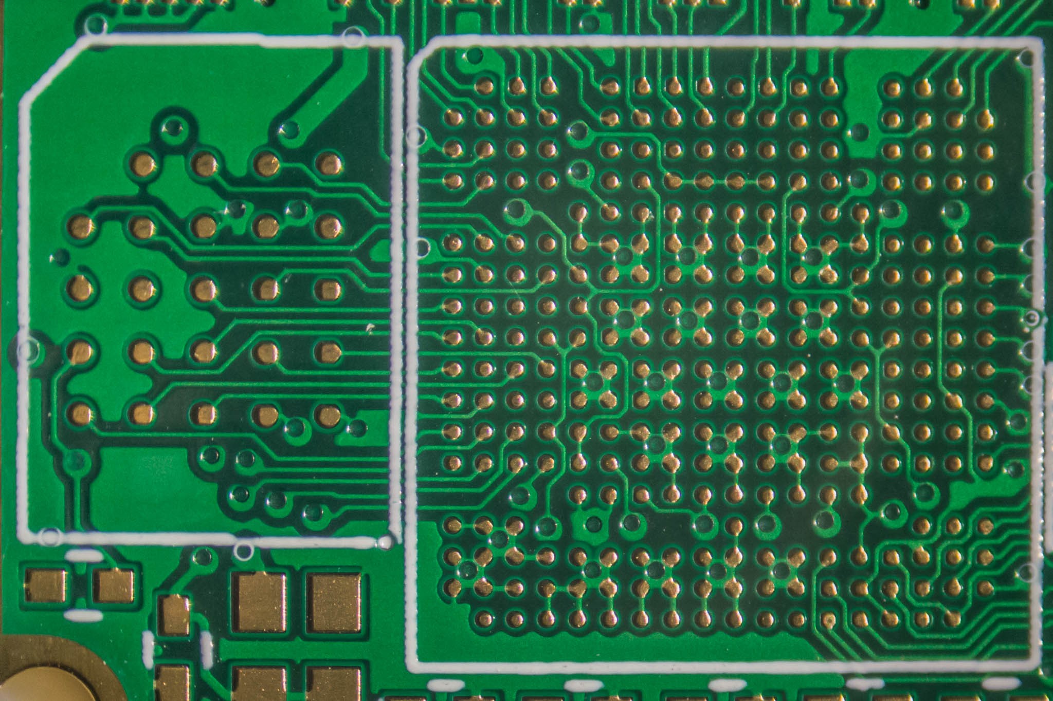
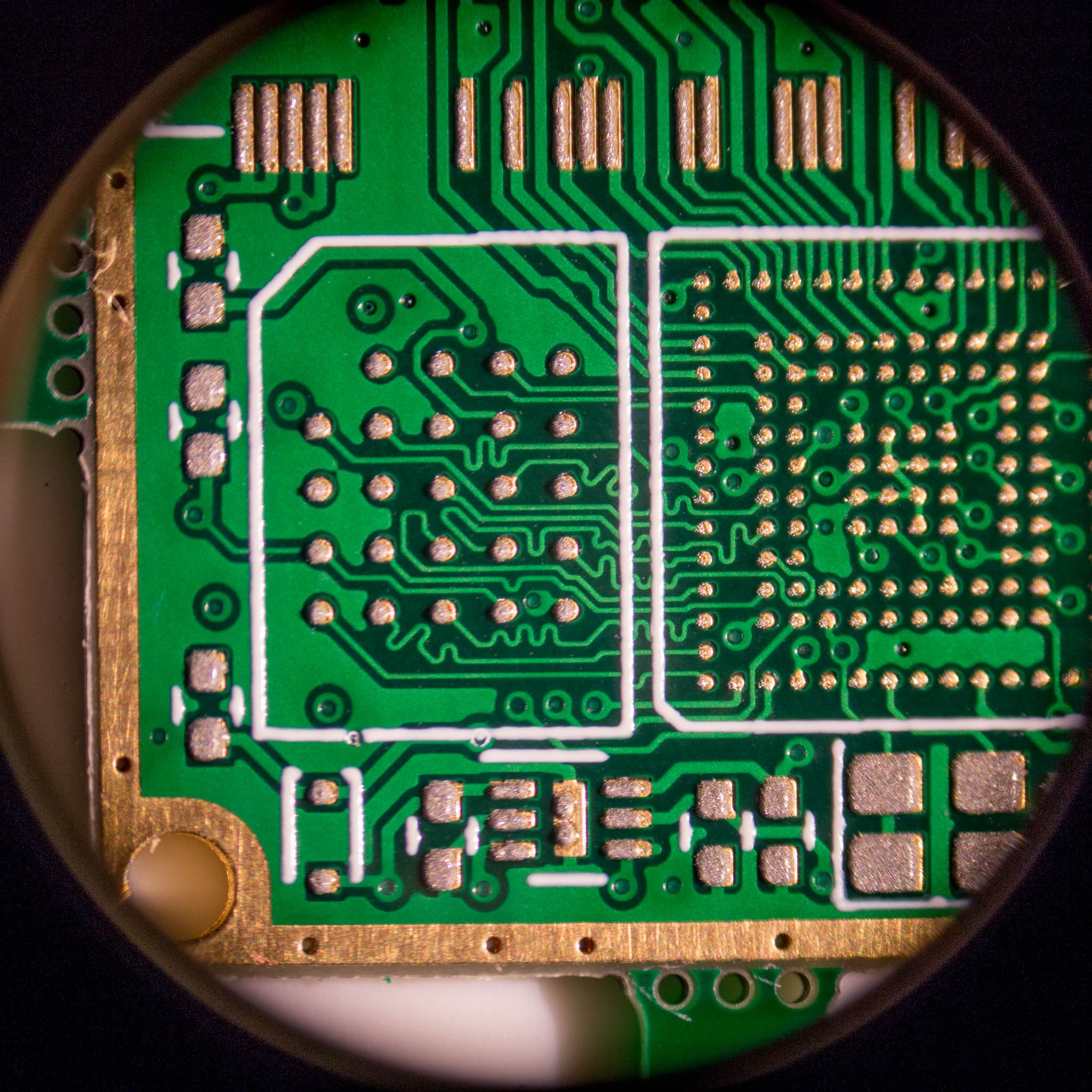
At this point I knew this MIGHT just work. I was not looking forward to prototyping a PCB that required a HDI PCB. But luckily it is possible to route out the connections required on a "basic" 3.5/3.5 0.2mm drill PCB process. This is due to the fact that the majority of the 285 balls in the center of the device are grounds.

It's not super pretty, but it should work. I did have a little trouble with JLCPCB accepting these files, initially they rejected the board. And I couldn't manage to explain to the support engineer that my project did in-fact meet the specifications set out on their website. I submitted the same design again, but also started to rework the design to improve clearances. Strangely they accepted the files without an issue the second time around. (I've since heard this is quite common)
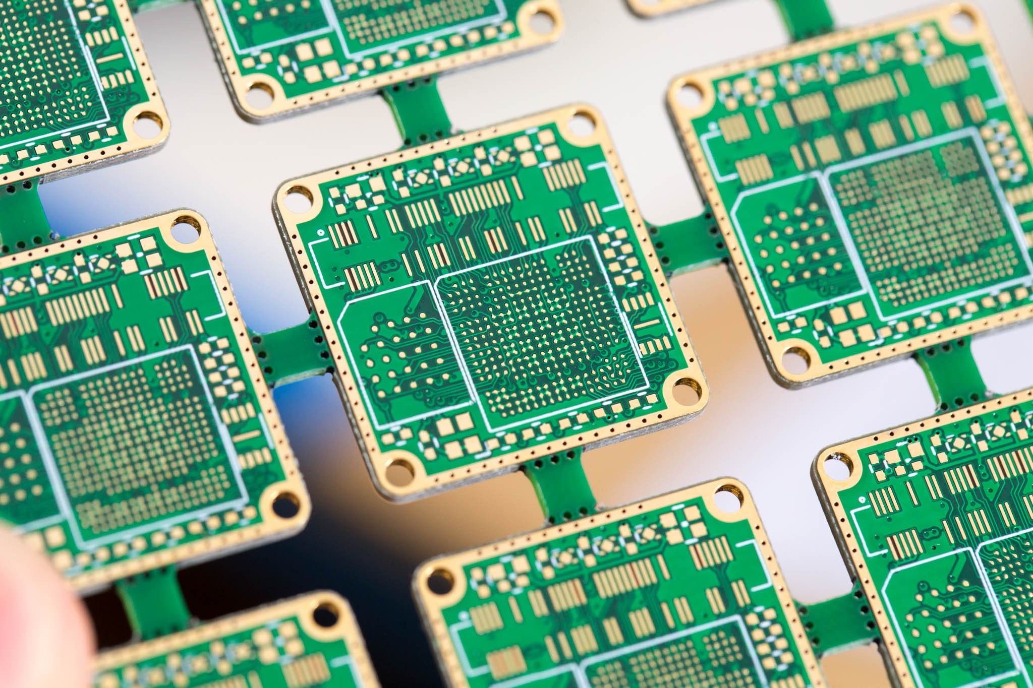
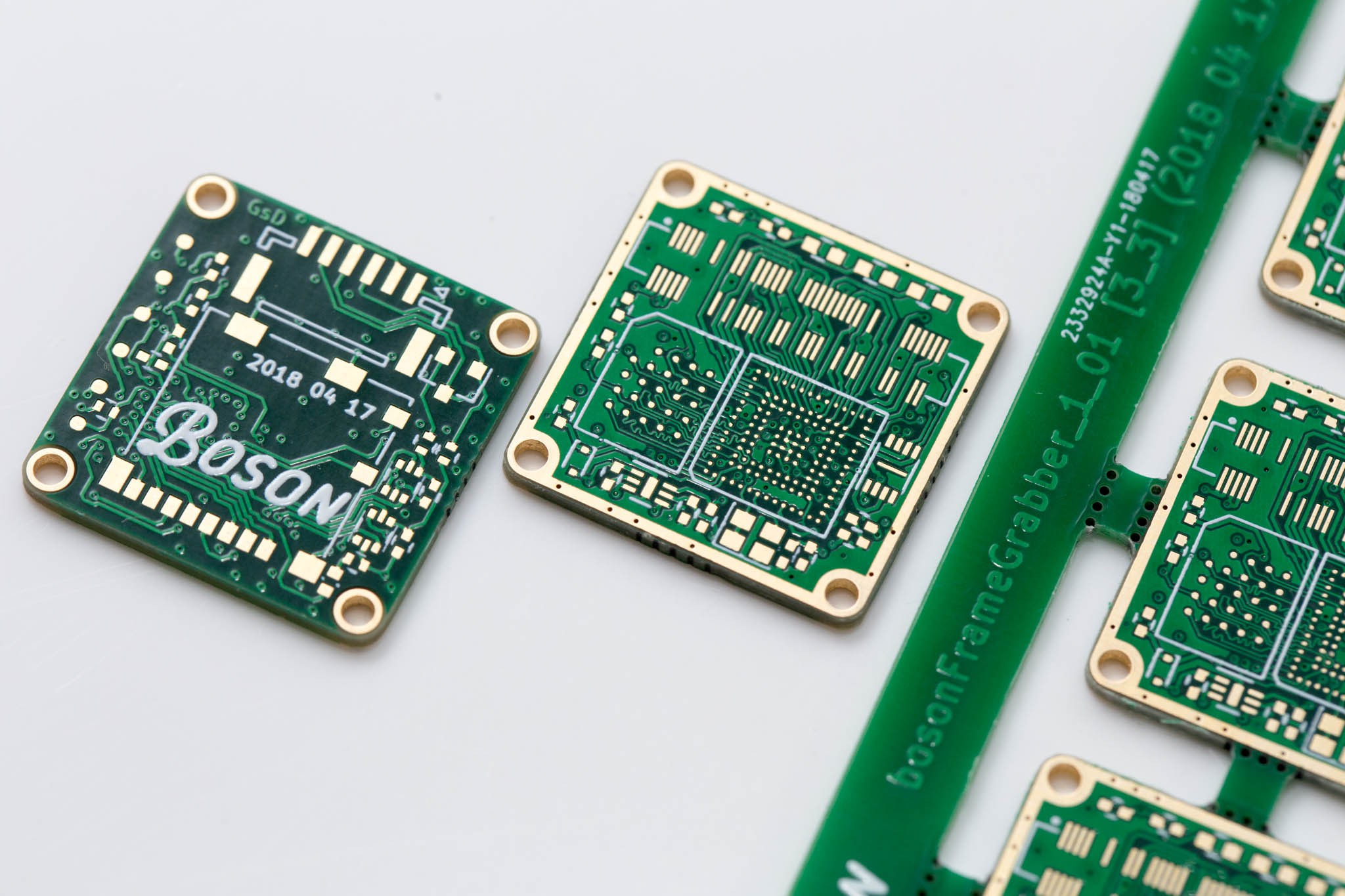
 The panels came back looking great! I'm panelising because the design is so small, I can fit 9 copies within 100x100mm. Which gets me their special prototyping price. Since the designs are all the same there is no surcharge for doing this. I'm using this paneliser: http://blog.thisisnotrocketscience.nl/projects/pcb-panelizer/
The solder mask registration is slightly off (But still VERY good) these boards should work great for prototypes. If the design works I would be very tempted to try out a board with plugged 0.15mm vias, eurocuircuts lets you cost this up on their online calculator. Since my PCBs are so small the cost per board is actually really good, but there is a steep one time NRE fee.
So far this version of the PCB was going great. With boards in hand I decided to order the BOM and assemble up a prototype.
That's when I found out the cs285 package of the ECP5. The package I needed. Had an 8 week lead time.
-
Prototypes 1,2,3...
09/09/2018 at 04:29 • 0 commentsI had mentioned in the last log that I created the footprint wrong for the HyperRAM device. Well my first bosonFrameGrabber PCB had the same errata.
 ---------- more ----------
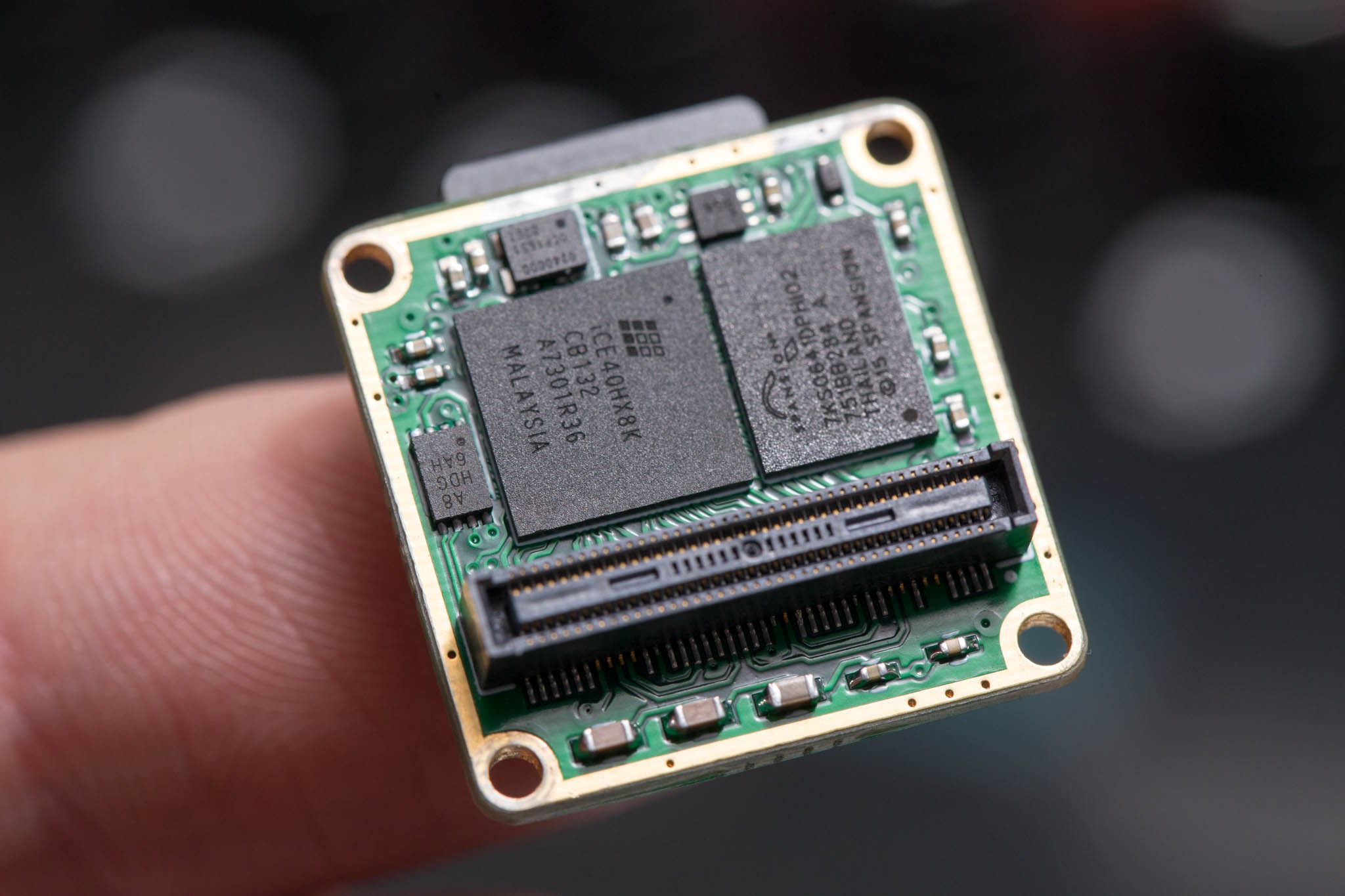
I was able to use this board as a test of my BGA soldering. I'd only ever soldered 0.8mm pitch BGA packages, and the HX8K was in a 0.5mm pitch package! Additionally in order to reduce board size I required a pogo-pin based JTAG connection. Luckily they did not have any errata, and worked great! (My FPGA JTAG programmer is a custom breakout for: https://github.com/esden/ftdi-multitool)

v1_01
This version had an updated HyperRAM footprint, and was also my first time ordering form JLC PCB. Surprisingly their standard service handles the 3.5/3.5mil trace/space and the 0.2mm drill required for the 0.5mm BGA pitch.

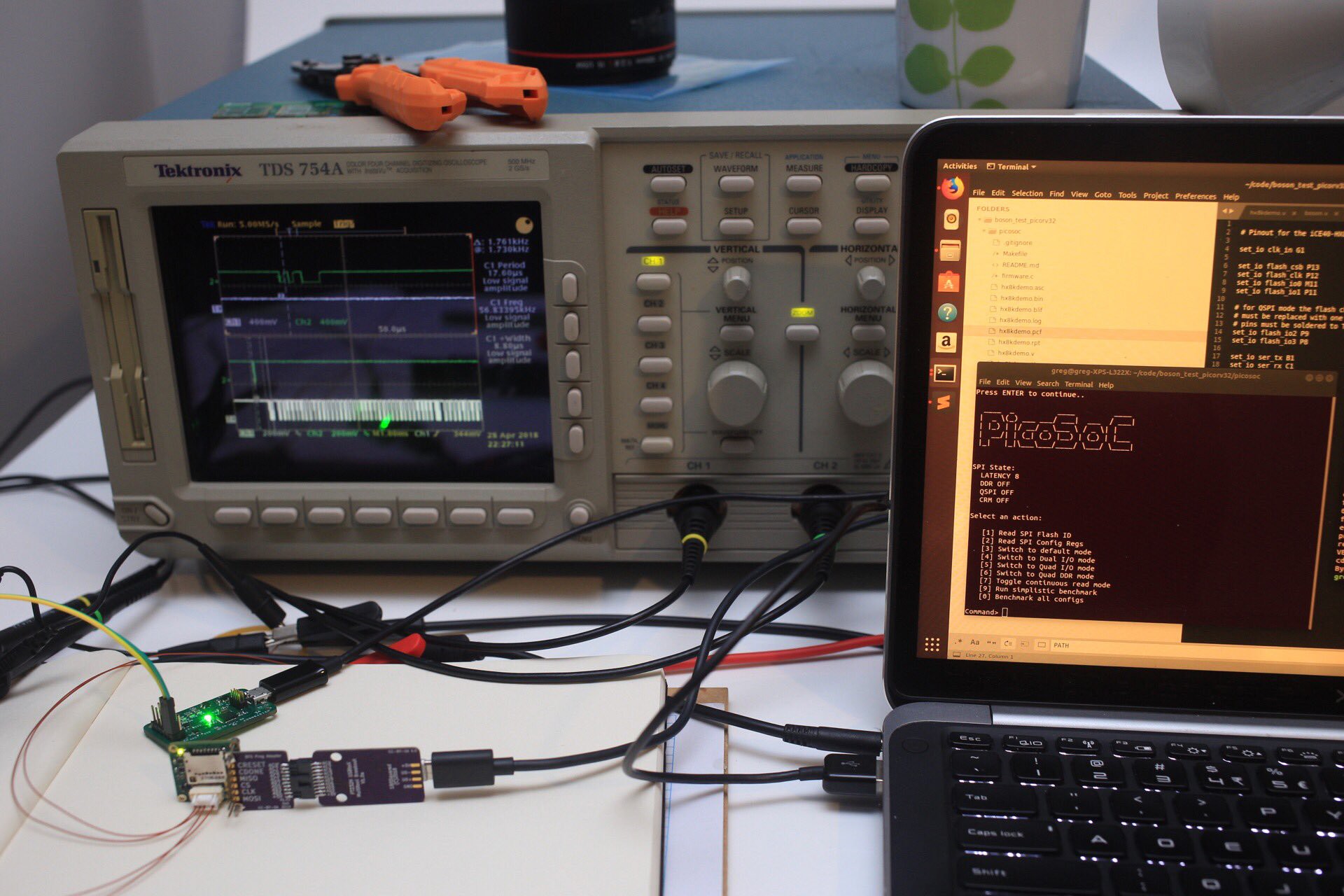
This version actually worked! I was able to port the example project of picosoc over very easily! (https://github.com/cliffordwolf/picorv32/tree/master/picosoc)


Working ontop of a working example is great. Really gives you a nice sandbox to adjust bits and pieces. If anything breaks you can backtrack to your last commit to determine the breaking changes.

I especially like the basic example code included with picosoc. It's all contained in a single file, and creates a simple prompt that enable you to interact with your hardware though a serial terminal. Adding function stubs to the prompt is super easy. Especially for a firmware engineer like me, it feel safe and familiar.
Over the course of a week I designed up a simple verilog block to capture a parallel stream, GPIO register, hyperram wrapper (based off BML's excelent work https://github.com/blackmesalabs/hyperram)
With these pieces I was able to jump back into firmware, add a FatFs driver using bit-banged IO, and capture this image!

A few issues with this image. I have the endianess wrong in this capture, and I had missed a single DWORD (2 pixels) at the start. But considering how far I had come in a week, this was a success!
Also due to the Bit-Banged SPI SD card interface, this 320x256 pixel image, at 320kb in size (16bbp) took around 15s to save.Now to optimize!
-
Project Goals and Motivation and Background
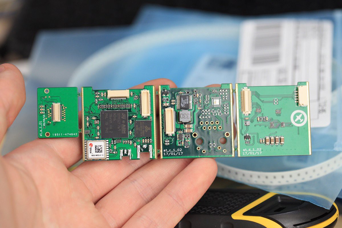
09/09/2018 at 03:44 • 1 commentAt my day job a few years ago I designed a reasonable small product that attaches to the back of a FLIR Tau2 thermal camera core. The product takes the digital video stream from the camera and saves this information to an SD card, it also included an ethernet 100MB/s interface. Since the Tau2 is a small camera, so the electronics in this product is made up of a "stack" of boards.

The Tau2 outputs a 14bit video stream of it's 640x512 pixel array. This stream needs to handle upto 60Hz on some product variants, so it features a 27MHz pixel clock. In order to ensure a frame from the camera was successfully captured I designed in enough memory to fully buffer a frame (> 640kb). It's design was based around an ARM M7 microcontroller. Utilizing external DDR memory and it's included 14bit Digital Camera Module Interface (DCMI).At the time I knew this was the perfect application for an FPGA, but having no hands on experience with them I decided it was too risky at the time.
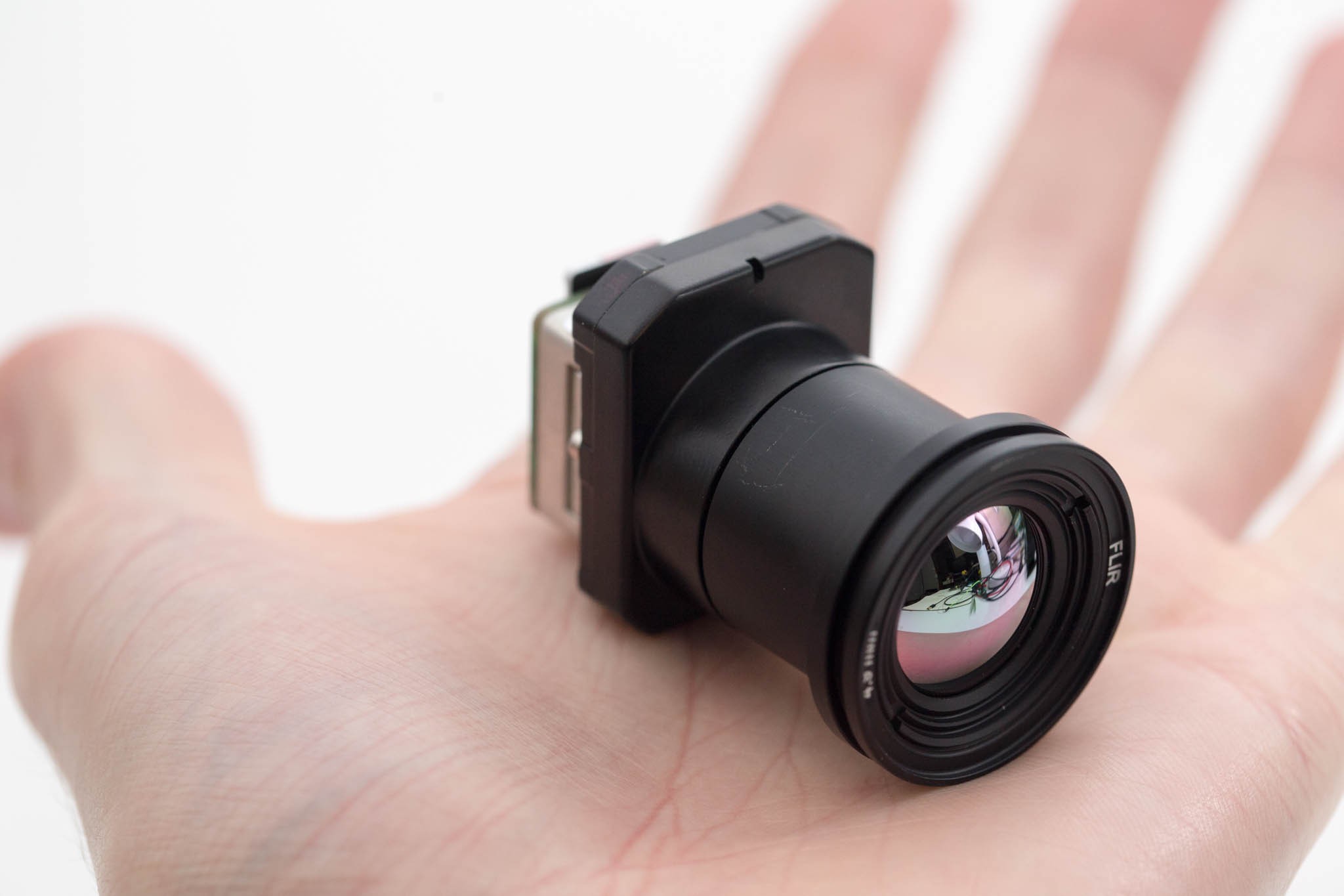
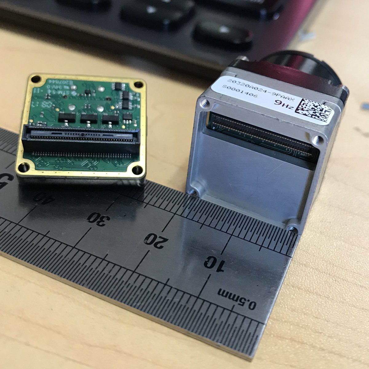
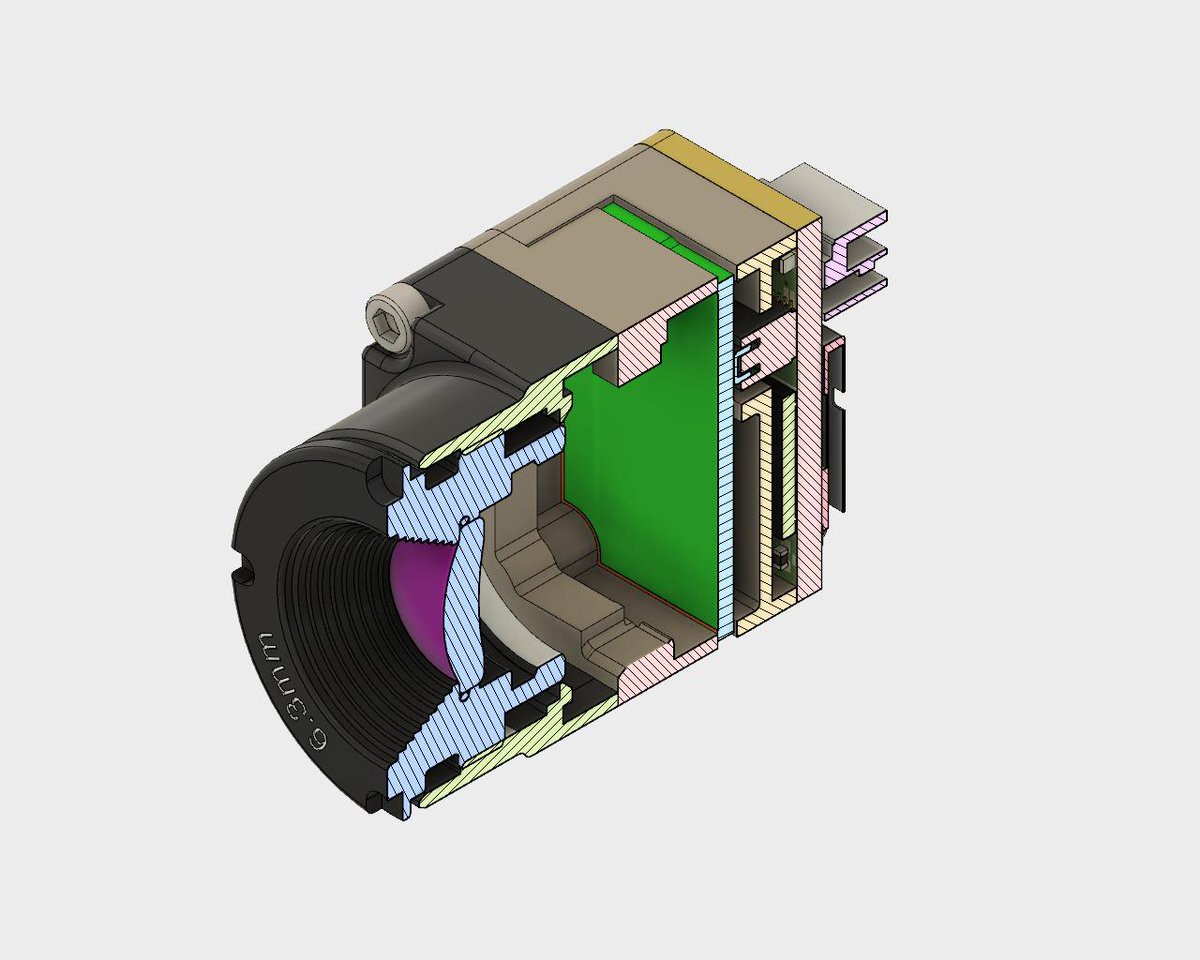
---------- more ----------Fast forward to Jan 2018. Our local FLIR rep had loaned us a FLIR Boson 320. The FLIR Boson is a tiny Thermal Camera core. Available in two variants: 320 and 640. These have an image size of 320x256, 640x512 respectively. When I say small, the footprint of the module is 21x21mm!!
FLIR made a nice choice with the interfaces, the Boson supports a USB UVC mode, which enable it stream digital video over USB natively. It also has a 16bit digital video bus, and Analog output. FLIR sells the USB module as "Back" for the camera. Which connects to it's 80pin interface connector.

As a bit of a challenge I decided to teach myself FPGAs with a hands on project. The goal, a small FPGA board that could capture frames from the 16bit camera interface and save these to an SD card. I'd only had experience with FPGAs in a class at university, that certainly gave me a solid understanding of fundamentals, but I'd never actually built an entire project with an FPGA before, how hard could it be?
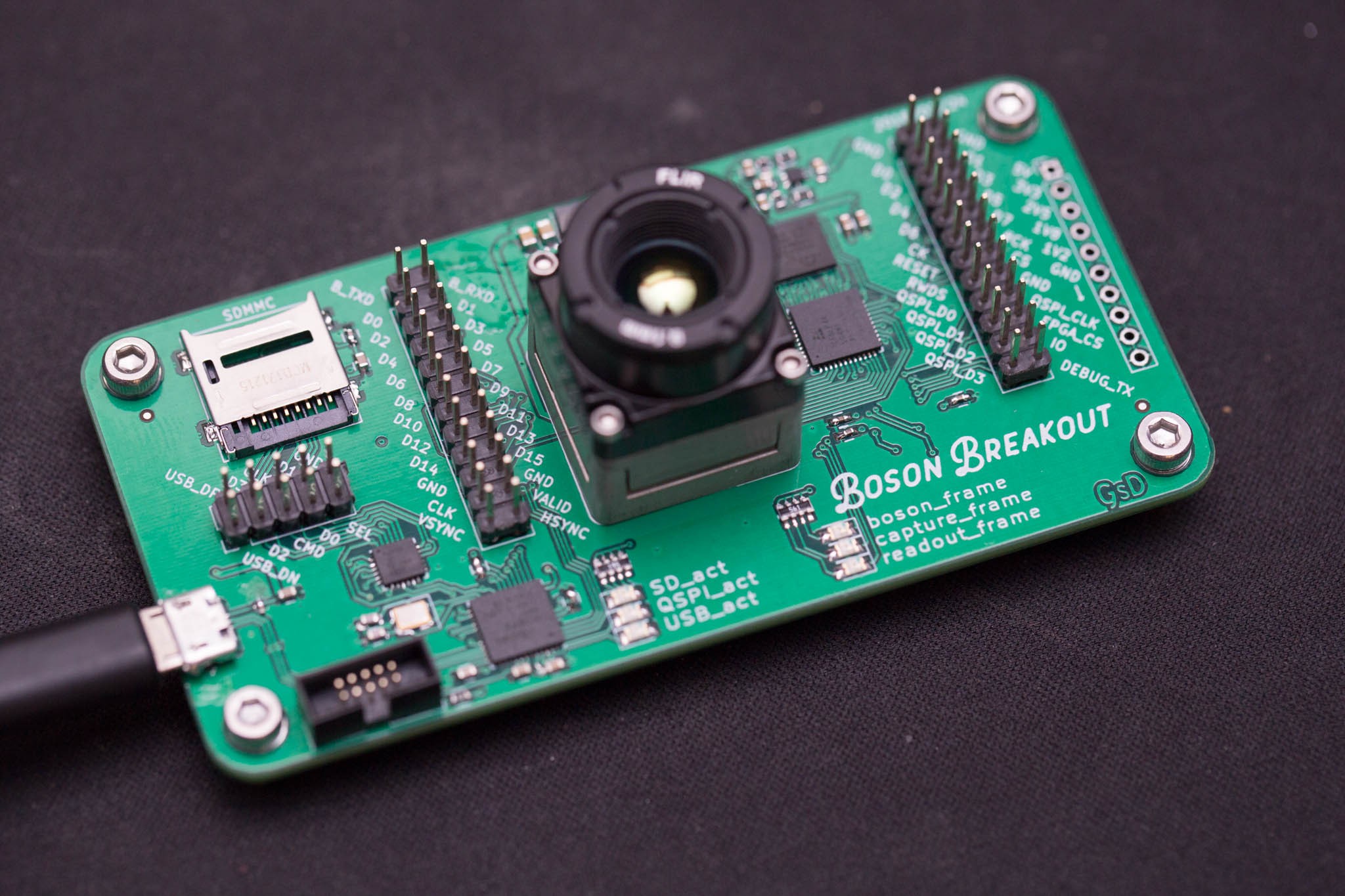
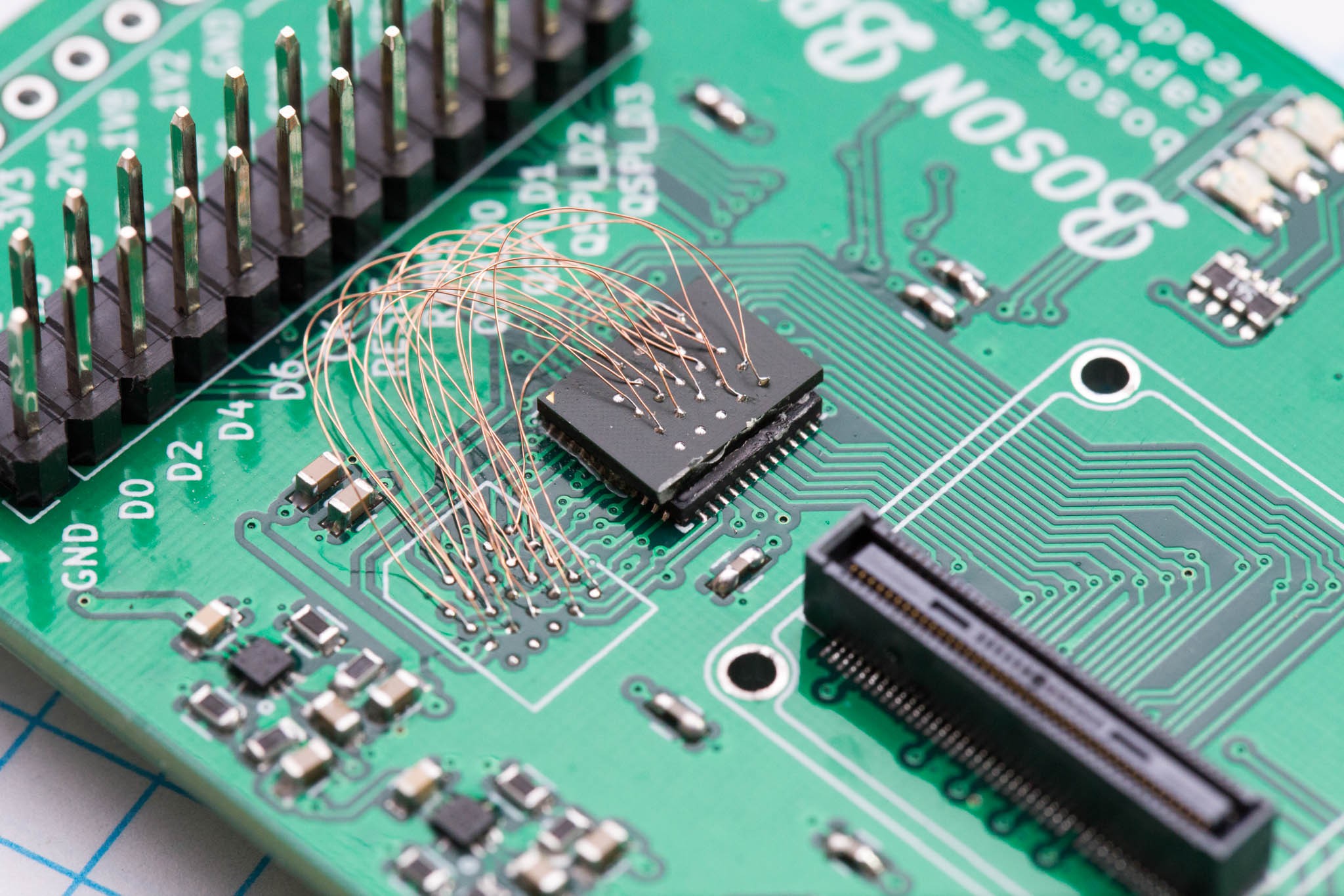
My first idea was to create a hybrid, FPGA/MCU device. The FPGA would be responsible for capturing the fast asynchronous data from the camera storing it external RAM. Then a standard micro-controller could read this data and save it to an SD card. I called this attempt the "Boson Breakout".

Unfortunately this board never really worked, the firmware remains unfinished. The concept SHOULD work, but there are too many bits and pieces. I also got the footprint wrong on the RAM. ouch.

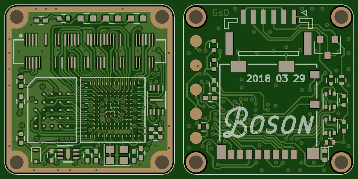
Parallel to "Boson Breakout", I had been researching project icestorm. An open source tool chain for Lattice FPGAs. I unfortunately had used a non-supported Lattice FPGA on my Boson Breakout. Which looking through the offerings of FPGA packages I found the perfect part! The Lattice iCE40HX8K in a 8x8mm package! Combined with a 8Mbit HyperRAM 6x8mm, I might be able to fit everything BEHIND the Boson camera....

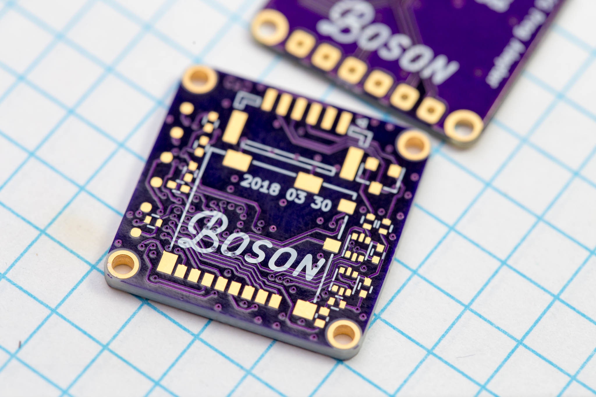
After a late night inside KiCad I had this design. A project was afoot!

Boson Frame Grabber
Simple FPGA based PCB to capture thermal images from a FLIR Boson camera on to a microSD.
 greg davill