-
26th August: Mechanix - enclosure design
09/30/2018 at 20:53 • 0 commentsI can't just stand there and watch Alex doing his magic on the bits and bytes, so I'm thinking of some king of enclosure for the locator.
- It must be small enough to be able to fit in small drones.
- It must be big enough to accommodate a 100-200mA LiPo cell and some kind of connector.
- It needs a transparent window, to be able to see the charging and the alive leds.
- The button needs a plunger.
- It will be 3D printed ! At the workplace, we have a Stratasys 260 UV-cured inkjet printer that sits around all day. The raw enclosure will be black, as this is the only ink available right now on the printer.
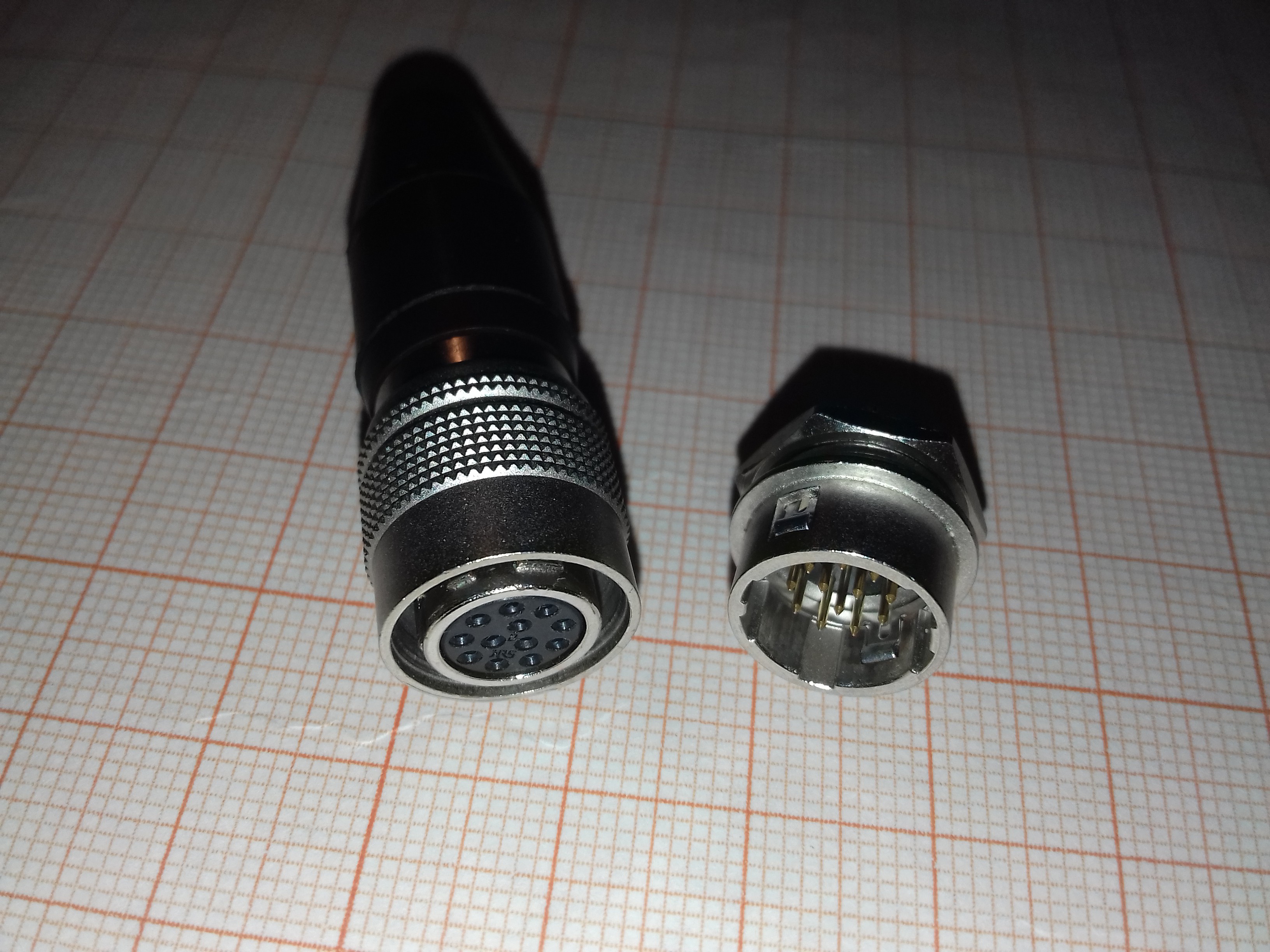
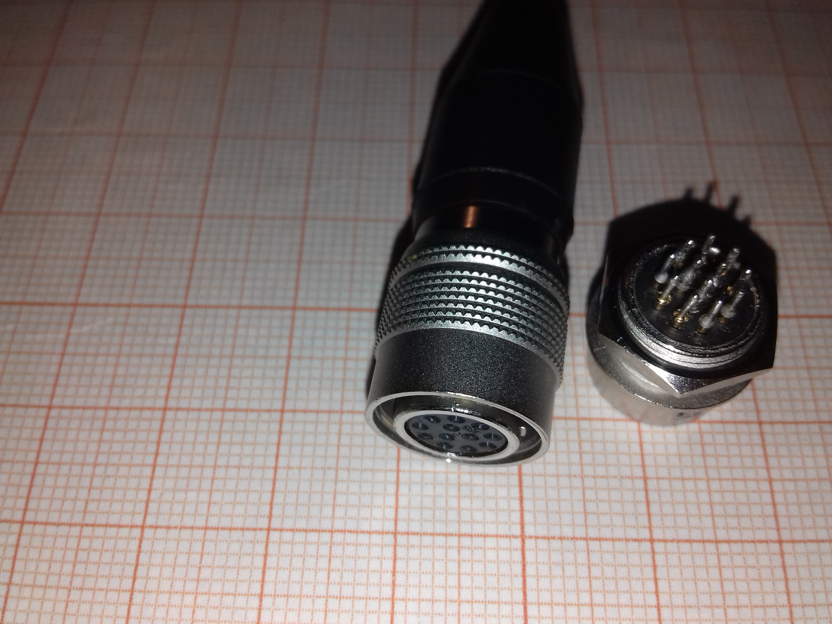
We modified some high end machine vision cameras for some customer and we have salvaged some nice connectors. It turns out that Hirose HR10A 12 pins circular connectors are fairly common, and not exaggeratedly expensive. I have two pairs lying around. Here are some close-ups:
![Fig. 1: HR10A pair. Fig. 1: HR10A pair.]()
Fig. 1: HR10A pair. ![Fig. 2: HR10A pair. PCB termination for the male part. Fig. 2: HR10A pair. PCB termination for the male part.]()
Fig. 2: HR10A pair. PCB termination for the male part. It looks and feels too god to let go.
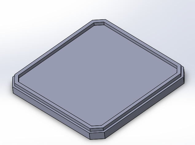
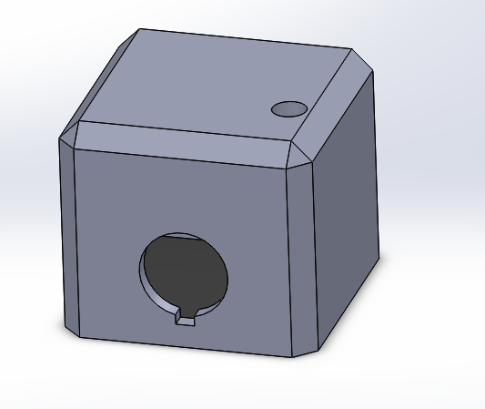
I started SolidWorks-ing an enclosure. It's work in progress, so don't jump to conclusions.
Fig. 3: Enclosure bottom. FIg. 4: Enclosure top. The round hole at the top is for the button plunger and the one on the wall is for the HR10A panel connector. Still a lot to be done...
-
25th August: Brain-power !
09/30/2018 at 20:22 • 0 commentsI miss it and i need it!
I am not very fast when it comes to programming, as a matter of fact I am really slow. I am that slow that I need help to finish this project on time. That's why I asked Alex from Embedded programming to help me out. He works all day with STM32 MCUs, so reading an UART interface and sending a packet of data every 10 seconds should be a breeze.
Unfortunately, he does not have an account on Hackaday, so I cannot add him in the "team".
Thank you Alex!
-
24th August: Boards completed
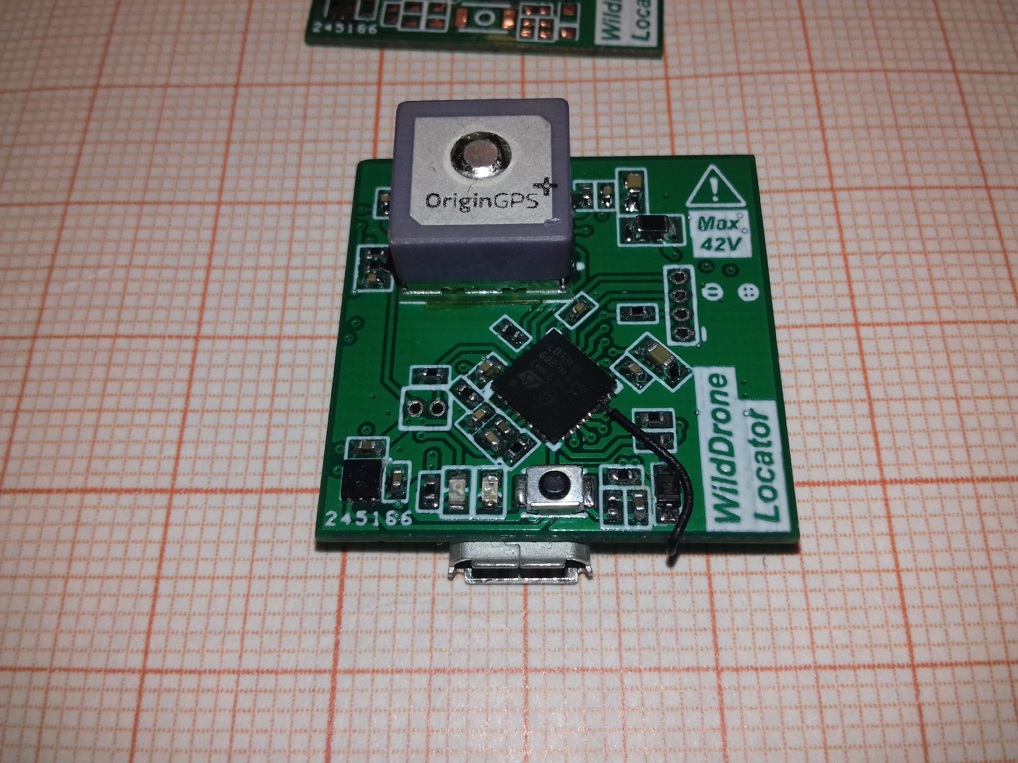
09/30/2018 at 20:08 • 0 commentsTook me almost an entire day to mount all 67 components.
An of course there had to be a bug. In fact two:
- If you look carefully at the bottom of the GPS module, you will see a bit of yellow kapton tape. It's because that huge pad below the component should have been covered with solder mask. And it's not. The module has some exposed metal pads below it, and they're not just ground pads.
- And that wire supposed to be included in the schematic. It connects DIO0 pin from the LoRa transceiver with a MCU pin (in this case PB11). DIO0 is the interrupt pin of the transceiver, and it signals various events to the MCU. I obviously found this out after sending the PCBs to the factory. Well, live and learn....
![Fig. 1: Kapton tape below GPS and a wire. Fig. 1: Kapton tape below GPS and a wire.]()
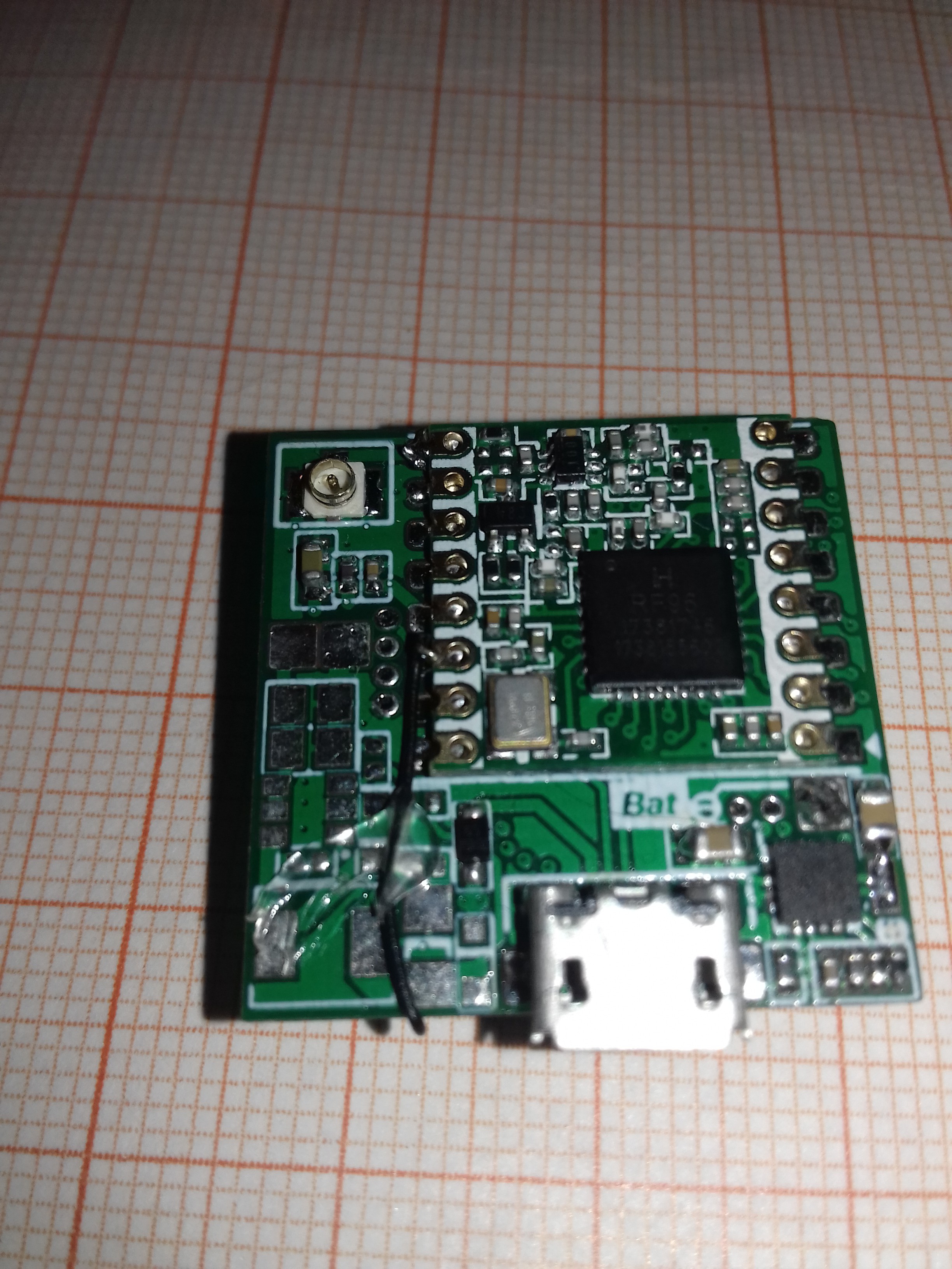
Fig. 1: Kapton tape below GPS and a wire. ![Fig. 2: That wire.... Fig. 2: That wire....]()
Fig. 2: That wire.... This particular board will be the receiver and it will be powered via USB, so the step-down converter is not attached (fig. 2, left side of the board).
-
23rd August: Solder solder solder ...
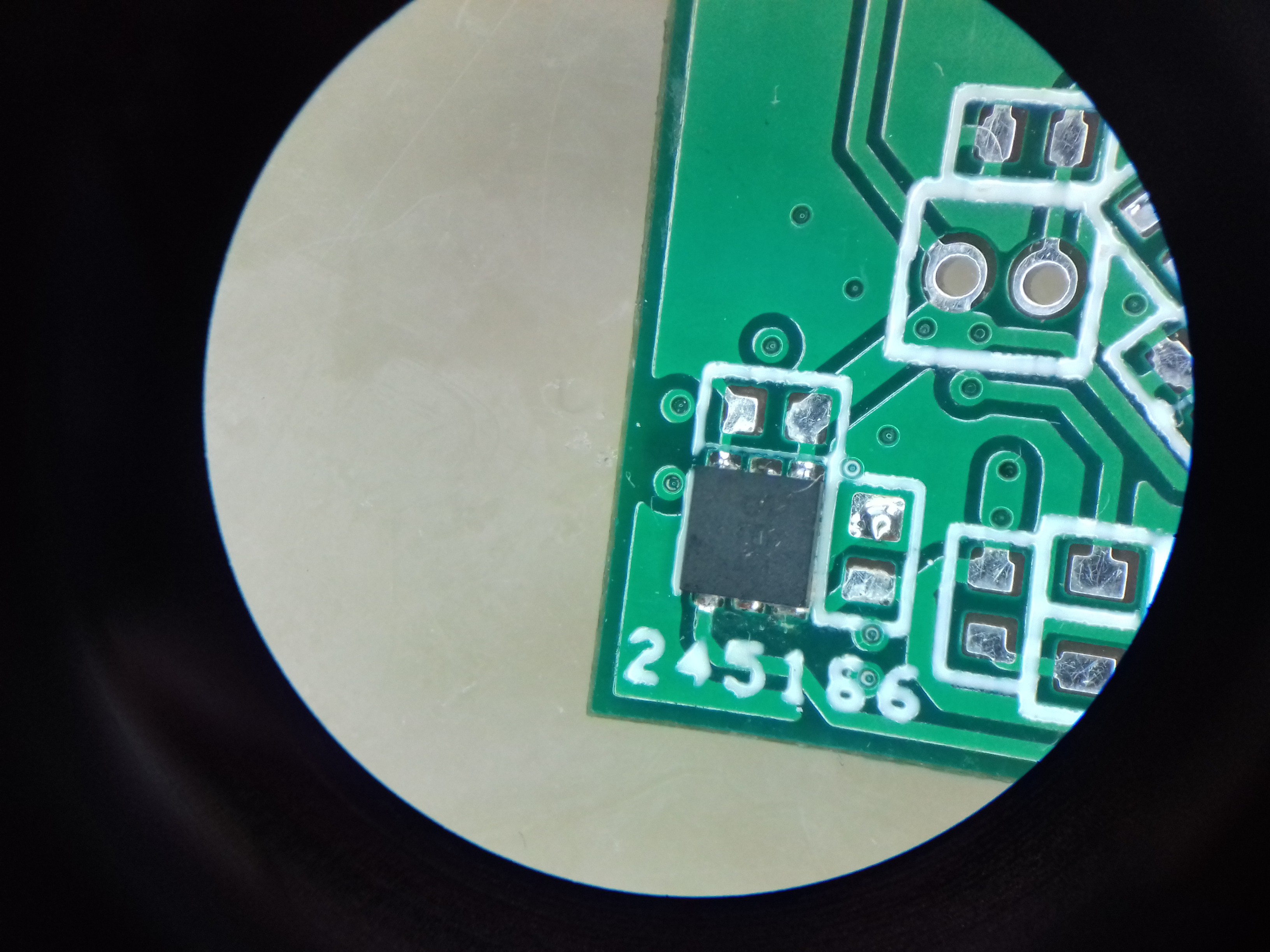
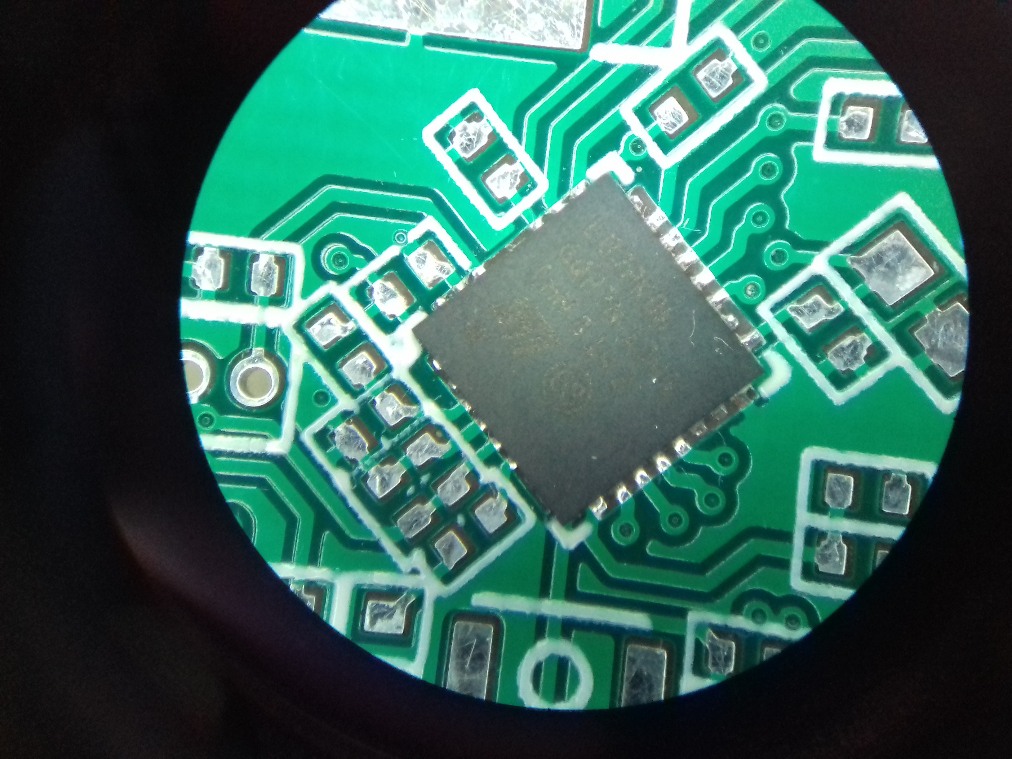
09/30/2018 at 19:48 • 0 commentsWhen I selected the tiny QFNs for the LDO and the MCU, I imagined it would be hell to solder them correctly. I was sooo wrong !
Check this out:
![Fig. 1: 3.3V LDO: 2x2mm QFN, with thermal pad. Fig. 1: 3.3V LDO: 2x2mm QFN, with thermal pad.]()
Fig. 1: 3.3V LDO: 2x2mm QFN, with thermal pad. ![Fig. 2: STM32L072KB: 5x5 mm UFQFPN, with thermal pad. Fig. 2: STM32L072KB: 5x5 mm UFQFPN, with thermal pad.]()
Fig. 2: STM32L072KB: 5x5 mm UFQFPN, with thermal pad. You need three things:
- Liquid flux: I used this.
- Hot air soldering station. The cheapest kind available is perfect.
- Cleaning alcohol, or acetone if available. It does a great job removing flux residue.
Here is how I did it:
- Turn your components upside down, to see the pins.
- Mount a needle on the flux syringe and place a small amount of flux on the component's pads.
- Holding the part with tweezers, place solder "cushions" on the pads with the soldering iron. It doesn't have to be a insanely small tip, the flux will not allow formation of solder bridges.
- For the exposed pad, place a smaller amount of solder. Too muck will make the component float on it and the pins will remain unconnected.
- Clean with alcohol.
- Repeat steps 2 - 5 for the pads on the PCB.
- It is important to clean flux residue on the pcb and component.
- Place FRESH flux on the PCB pads (an amount similar to the one used for tinning the pads).
- Place your component on the pcb. The flux stickiness will hold it in place. Make sure you centered the pins on the pads.
- Set the hot air station at the lowest airflow and at 350 deg Celsius (mine does not actually output 350 deg., but below this setting solder won't reflow). By the way, I used Sn60Pb40 solder wire.
- If properly aligned, the component will auto-position on the pads when the solder reflows. If not, while in liquid phase, gently move the component in place. If there is enough flux. it will "snap" into place.
- That's it!
The photos were taken with the phone stuck to a microscope eyepiece.
Alright, 2 components down (the most challenging ones), 67 more to go. I won;t be able to finish 2 boards today, so I'll be back tomorrow with fresh photos.
-
22nd August: They're here!
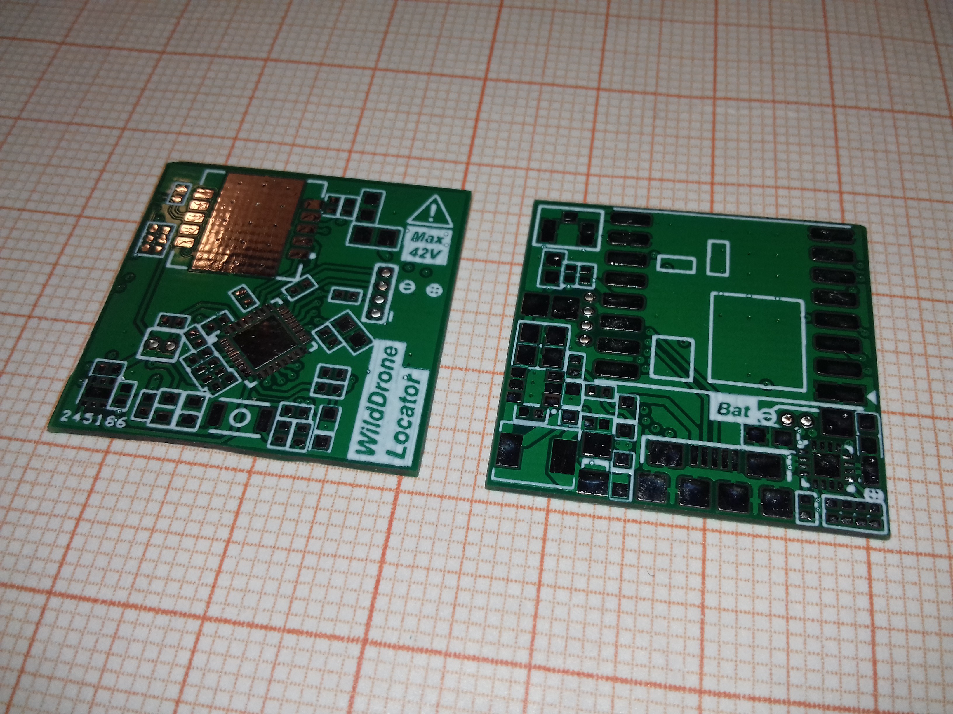
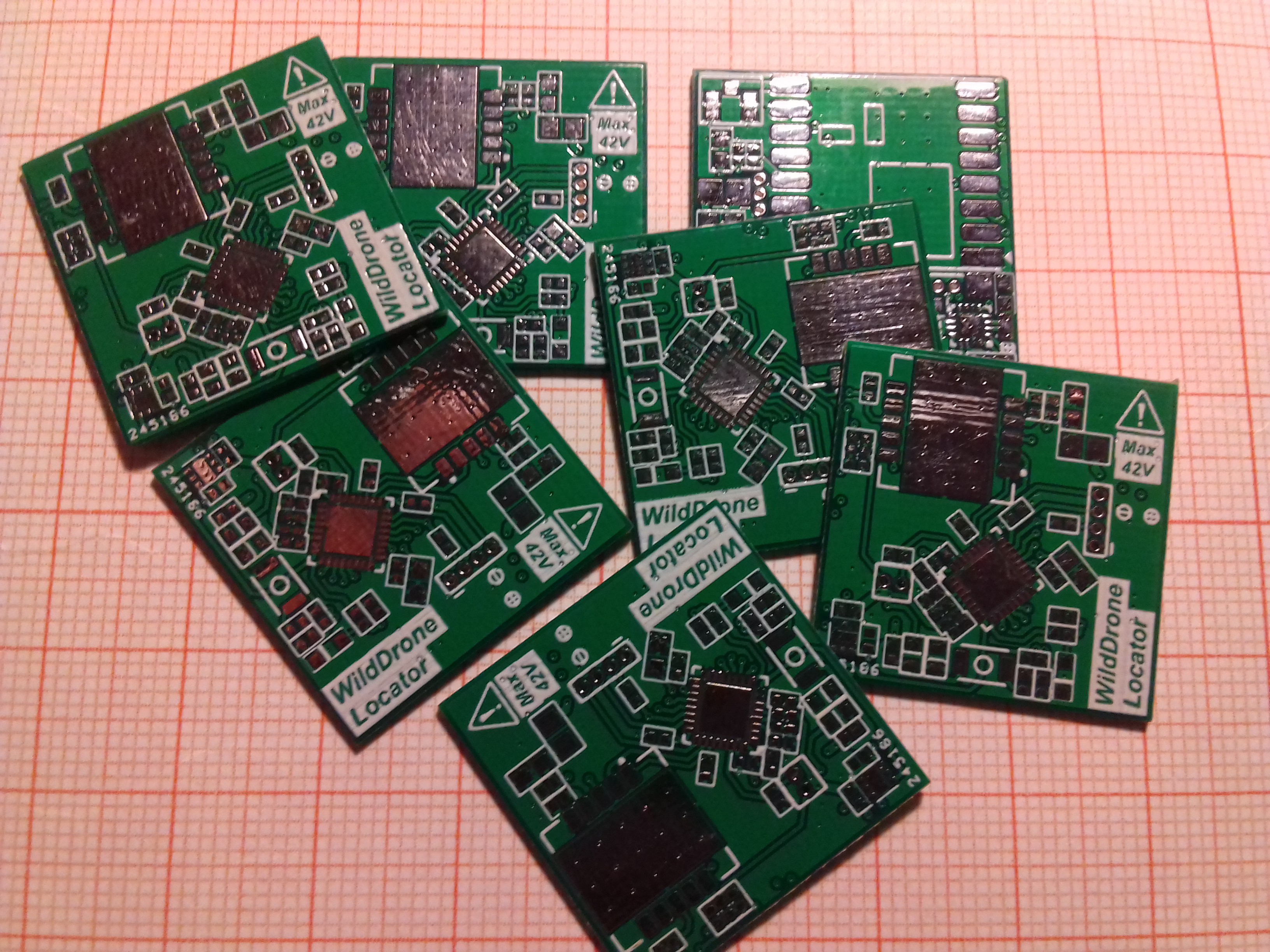
09/30/2018 at 19:24 • 0 commentsI am back, and so are the PCBs:
![Fig. 1: Top (left) and bottom layer view. Fig. 1: Top (left) and bottom layer view.]()
Fig. 1: Top (left) and bottom layer view. ![Fig. 2: Bunch of PCBs. Fig. 2: Bunch of PCBs.]()
Fig. 2: Bunch of PCBs. The components will arrive tomorrow. Time to fire up the soldering iron!
-
12th August 23:58: Out to Fab!
09/30/2018 at 19:14 • 0 commentsI just sent the PCBs to AllPcb. Hopefully they will arrive in one week. Fabrication time is 2 day and it usually takes around 3 days to arrive with DHL.
Won't be around until 20th of August.
-
12th August: Let there be PCB!
09/30/2018 at 18:00 • 0 commentsI must finish the PCB and send it to the fab today! I'll be away for the next week and I do not want to waste a entire week. I must also order the components to finish this on time!
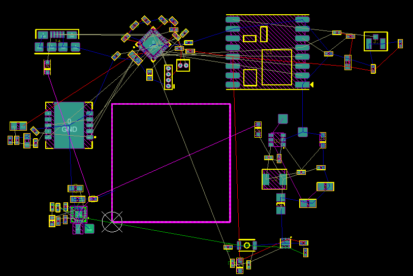
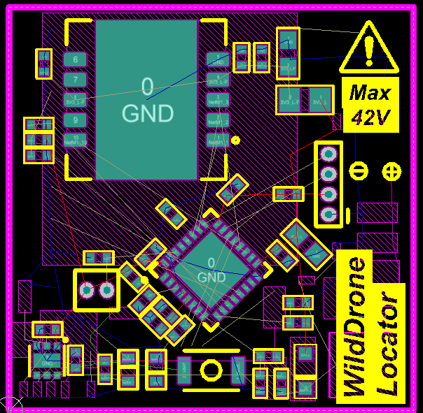
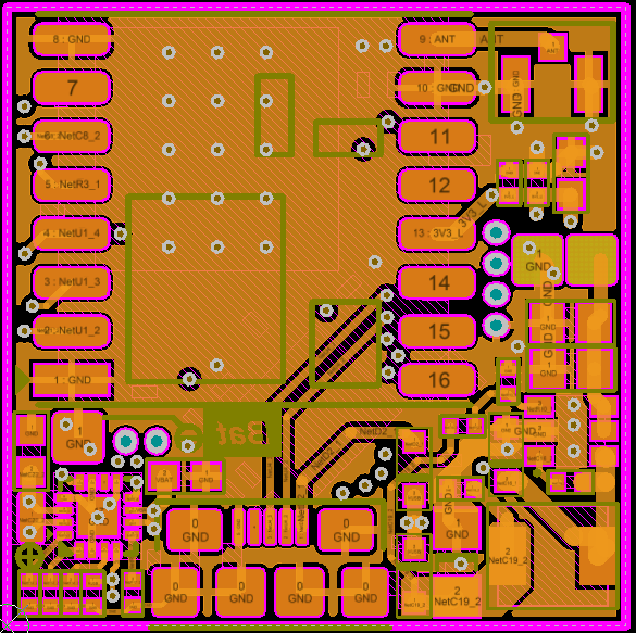
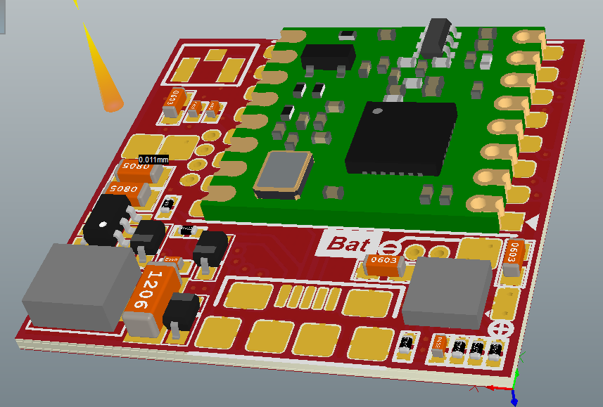
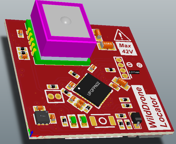
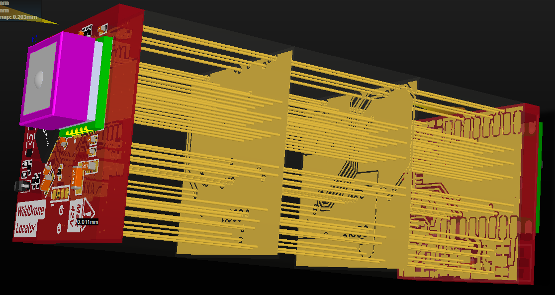
Here are some screen shots with the PCB in progress:
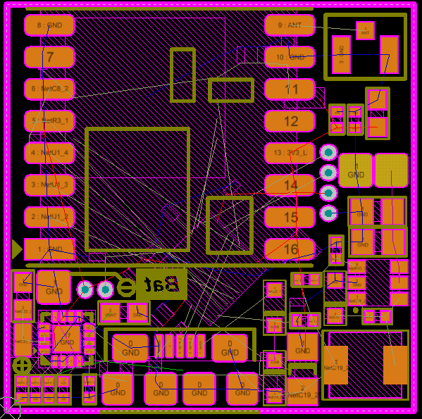
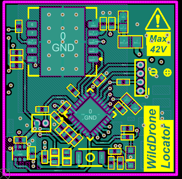
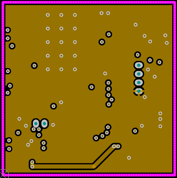
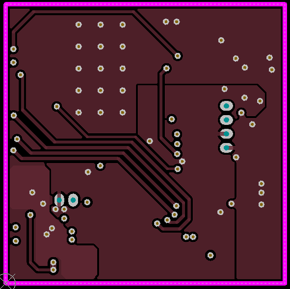
Fig. 1: A discouraging pile of components... Fig. 2: Components grouped by logical blocks. - After several attempts, they finally fit in ! Even found some room for sill screen markings!
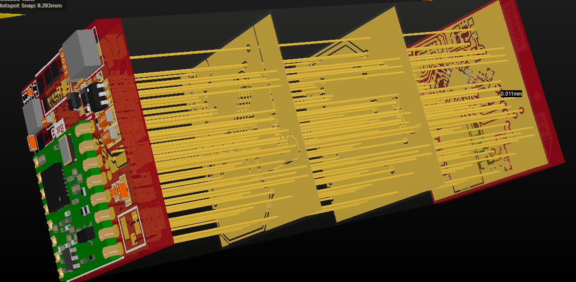
Fig. 3: Top component placement. Fig. 4: Bottom component placement. Fig. 5: Top routing. Fig. 6: Internal layer 1 routing. Fig. 7: Internal layer 1 routing. Fig. 8: Bottom layer routing. Fig. 9: 3D rendering, bottom view. Fig. 10: 3D rendering, top view. Fig. 11: Layer detonated view ! Fig. 12: Layer detonated view ! -
11th August: Schematix done !
09/30/2018 at 16:16 • 0 commentsYay! The schematic is not that complicated, it took me longer to create all the symbols and footprints!
Each block has its own schematic page. Let's start with the power block:
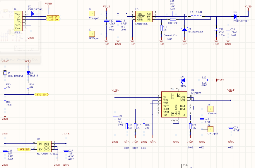
Fig. 1: Power block. - J4 is the micro-USB connector. The diode makes sure there is no reverse current in case of powering the locator via the step-down converter and the USB cable is attached to a shut-down device. Perhaps nothing happens, but you can never know... USBD+ and USBD- ports connect to the MCU.
- Power for the buck converter comes from two pads. The output of the LMR14206 is also isolated through a diode, to prevent reverse current.
- The NCP705 is straight-forward: 1uF input and output capacitor and a direct conection to the MCU for Enable.
- The BQ24072's input current is limited at ~500mA using the 3K resistor (R17). The charge current is set by R16 at ~200mA. I limited the input current at 500mA because the charger can power the circuit and charge the battery at the same time. I intend to use a 200mAh Lipo cell (so 1C charge rate). The rest of 300mA are reserved for the load: 120mA for the LoRa TX burst, and 55mA for the GPS module. The rest is headroom for the MCU. I also enabled the timer: if the battery is faulty and it doesn't reach end-of charge voltage in 3 hours, it declares the battery as dead and it blinks the CHG led so signal it.
- And now to the interesting part: the turn on circuit (center left, the one with the button). It is too clever to be my idea (thank you Alex !). Let's start with the 3.3V regulator disabled. Vbat is always available as 4V (consider the battery almost full). R15 keeps the EN pin of the LDO low. Pushing the button, the EN pin goes HIGH and enables the regulator. At this point, D5 and R14 keep the EN pin high. And that's it.
- The smart part is to use the same button to power down the thing. The EN pin also connects to the one input of the low power comparator of the MCU. The other input is connected to a reference voltage created by R5 and R6 on the MCU sheet, which outputs 3V. The divider created by D5-R14-R15 outputs a lower voltage: 1.8V. When you push the button, higher voltage comes from the battery and the comparator toggles. D5 is important because it does not allow high voltage on the 3.3V rail.
- The comparator triggers an interrupt and the MCU pulls down the EN pin of the 3.3v regulator. Of course, after you released the button.
- This way, I use the same button for hardware power-up and software power down.
Next, the MCU:
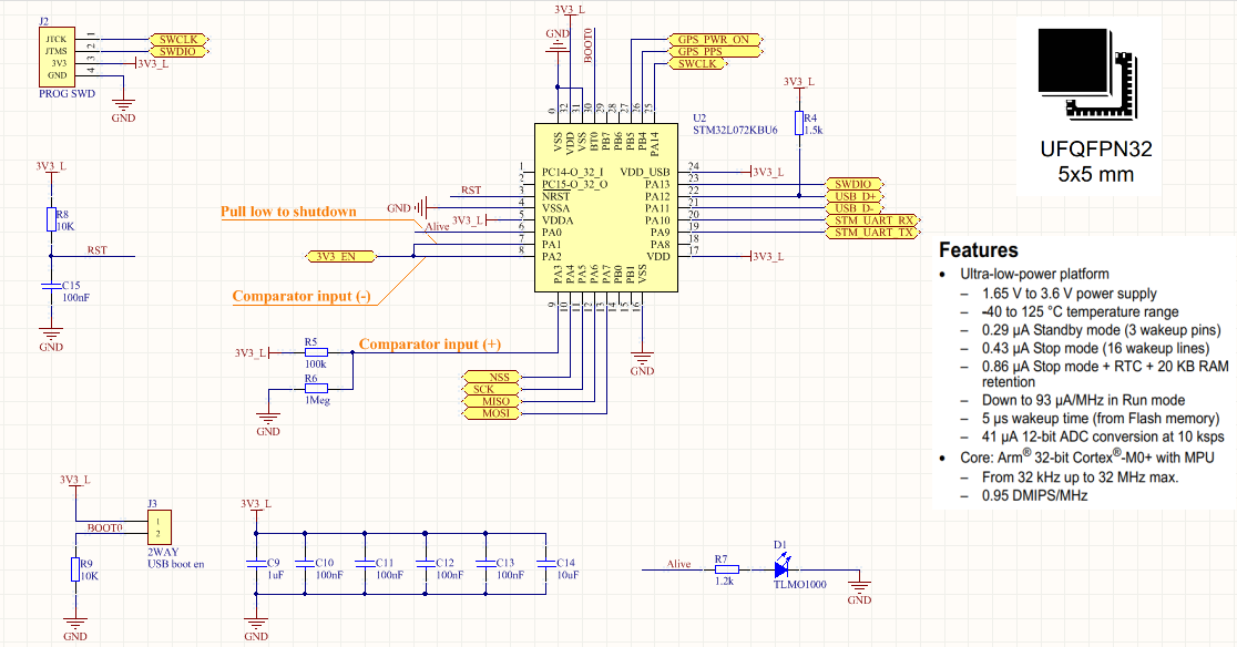
Fig. 2: MCU block. - J2 is the programming and debug connector: 4 holes 50 mils apart to accept a pin header. I will use the SWD interface.
- R8 and C15 keep the reset high.
- J3 and R9 change the boot option. If jumper J3 is fitted, the USB bootloader is enabled and a firmware update is possible.
- C9 to C14 are decoupling capacitors, as recommended by ST in the MCU datasheet.
- D1 lets you know that the circuit is operating.
- R5 and R6 create the reference voltage for the power-on and power-off circuit.
- R4 signals the USB host that a USB full speed device is connected.
Moving on with the GPS module. Nothing spectacular here:
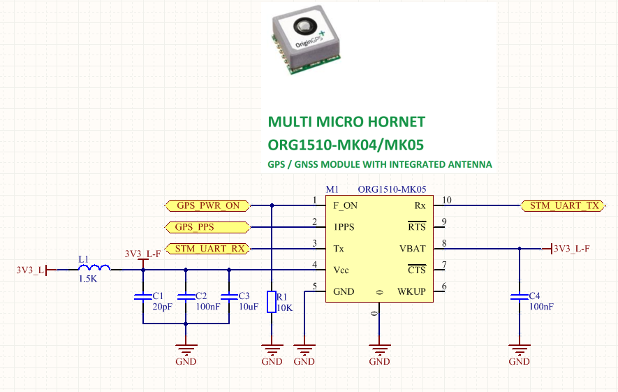
Fig. 3: GPS receiver. - L1 is a ferrite bead responsible for filtering conducted high frequency noise from the buck converter and the MCU.
- C1, C2 and C3, of increasing values decouple and filter even more the power line.
- There is no back-up battery at the Vbat pin, so a 100nF capacitor is required.
- R1 keeps the part in shut-down mode and it's enabled by the MCU.
And the LoRa Transceiver:
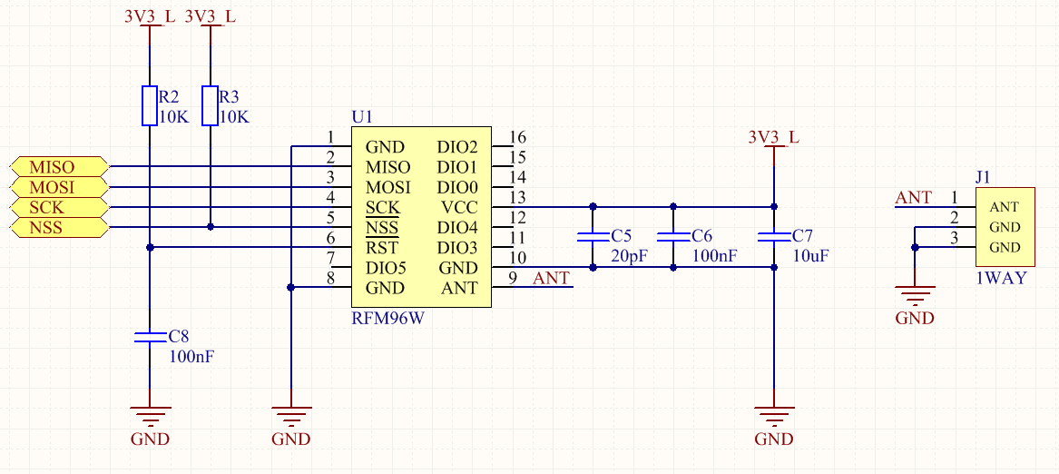
Fig. 4: LoRa transceiver. The reset and the CS pin are kept high by R2+C8 and R3, respectively. The same combo of different value capacitors decouples the part.
On the left is the UFL connector.
Now let's proceed with the PCB layout. I am seriously considering a 4 layer board. I do not want to lose GPS fix when sending LoRa packets ...
-
9th August: Component selection
09/30/2018 at 15:05 • 0 commentsToday I have been searching for components. Took a while. Here is the selection:
- High voltage step down converter: LMR14206 made by Texas Instruments. Its maximum input voltage is 42V, it switches at 1.25MHz and outputs 600mA. It also has a small package (SOT23-6) and a low component count: one ceramic input capacitor, 2 resistors for feedback, one bootstrap capacitor, an electrolytic output capacitor and, of course, an inductor. 15uH is the recommended value, also confirmed by calculation.
- 3.3V LDO: NCP705. Provided by OnSemi, this tiny regulator is low-noise, low Iq and high current (500mA). Did I mention it is tiny ? It's only 2x2mm. I hope it won't be impossible to solder. The price certainly got me convinced: only 0.85$. And it also has an Enable input. I obviously got the fixed 3.3V version.
- LiPo charger: BQ24072 claims to be "USB-friendly". After reading the datasheet I understood why: it regulates its input current to avoid bringing down the entire USB power line. Long story short, if you set it to charge with 1A but you plug it in a 500mA USB port, instead if drawing 1A to fry your port, it will reduce its current to keep the 5V line up. I initially wanted to create the battery switch-over with diodes, but it won't be the case anymore. This chip includes PowerPath circuitry. If you feed it with 5V, current will go to your load and also to your battery, so you can turn on your toy even if the battery is completely dead. The circuit takes power from the 5V line, but if removed, it automatically switched to battery power. A tiny 1s LiPo UPS for just 3$.
- Micro-controller: STM32L072KB caught my eye instantly: ultra-low power, small package (QFN32, 5x5mm) USB bootloader pre-programed and low power analog comparators (there's a catch here...). Might be a bit tricky to solder, especially with the exposed pad beneath, but I'll take my chances with a hot air gun.
- GPS: of course it would have been easier if I searched the internet for "world's smallest GPS module" but I had to take the long path and search at multiple manufacturers. Many had small receivers, but only one included a proper antenna on top. Hornet series from OriginGPSis made up of various modules, but the ORG1510 is the only one that communicates using 3.3V levels. All others use 1.8V. I selected the ORG1510-MK05, because it was the only one in stock. Fairly pricey. But small: 10x10x6.1 mm.
- Finally LoRa: RFM96. Not the cheapest radio module out there, but Andreas Spiess' post convinced me. From his video, line of sight is very important for long range LoRa transmissions (for any transmission, in fact), and, as my locator will be placed in drones and gliders, it won't be a problem. Found it at the same supplier I got the GPS, at 13$.
- And of course, lots of passives: I will use 0402 components where possible. More of those after the schematics.
Having my components, I can start working at the schematics. Bye!
-
8th August: Block schematic
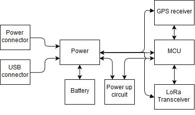
09/29/2018 at 19:16 • 0 commentsNow that I have my requirements set up, I can plan my circuit using a block diagram (fig. 1).
![Fig. 1: Block diagram. Fig. 1: Block diagram.]()
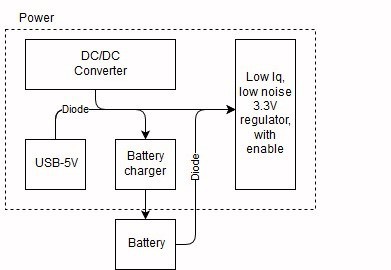
Fig. 1: Block diagram. The power circuit is fed in 2 ways: 5V from an micro-USB connector (also used for programming and configuration) and whichever voltage comes from the drone's power system. The power block is detailed in fig. 2. It contains:
- a DC/DC converter that steps down the voltage to 5V. The converter 5V is separated from the USB 5V using 2 Schottky diodes.
- a battery charger. Since all electronics run on 3.3V, a single LiPo cell is enough. The charger will be of linear kind, with low charging current (the battery will also be small), compatible with PC USB ports (max 500mA current draw).
- The battery is also connected with a diode for fast switch-over in case the other sources disappear. It would be nice if the battery included its own cutoff board (such as the CX-10 mini-quad battery)
- a 3.3V, low quiescent current LDO, with enable input. I do not intend make use of the MCU's deep sleep modes instead of a hard shut-down. This way, I can also take advantage of the GPS' module low power tracking mode. It would be nice if I could fine one that also has low noise. Generally, the GPS receivers are quite sensitive and usually require less than 10 mV peak-to-peak noise on the power input.
![Fig. 2: Power block. Fig. 2: Power block.]()
Fig. 2: Power block. I haven't thought at the power up circuit yet, but it will certainly have something to do with a momentary push button and the micro-controller.
The MCU will be of ultra-low power type, most likely a STM32L0 with the smallest available package (except BGA and chip-scale package). USB peripheral would be nice, it could make the micro-USB connector more useful (for configuration and possibly firmware update). This block also includes everything a MCU needs: reset pull-up and capacitor, configurable boot mode (depends on the MCU), an "alive" led, decoupling capacitors and, obviously, a programming connector (probably smd pads to solder wires).
I will search for the smallest GPS receiver available, with low power tracking modes. Power down options (other than power cutoff) are also required, and most likely, will be an Enable pin, driven by the MCU.
I already selected the radio module: RFM96. It is a LoRa transceiver, operating in the 433MHz band. Apart from LoRa, it also knows FSK modulation, so it might be possible to send some audio, but that's a feature for the far away future. The antenna will be attached with a UFL connector.
Now let's find some real world components!
WildDrone Locator
"Safety First!", we often hear. Mounted on a drone, this beacon says "I'm here!" in LoRa language.
