-
Stage 4 Software
03/04/2019 at 14:27 • 0 commentsWith the addition of 32-bit wide, 16-megabyte DRAM, Tiny030 is capable of running a varieties of application software quickly. In this project we'll rerun the EhBASIC and memory diagnostic of Stage 3, add a new memory diagnostic for 16-meg DRAM, and do a benchmark of EhBASIC running in DRAM and compare that to EhBASIC running in 8-bit RAM.
The existing ROM monitor runs fine in stage 4 hardware. It now can access memory located from 0x1000000 to 0x1FFFFFF.
![]()
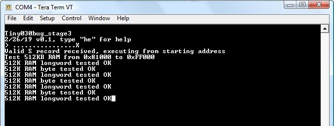
I wrote a memory diagnostic to test 16 meg of DRAM
![]()
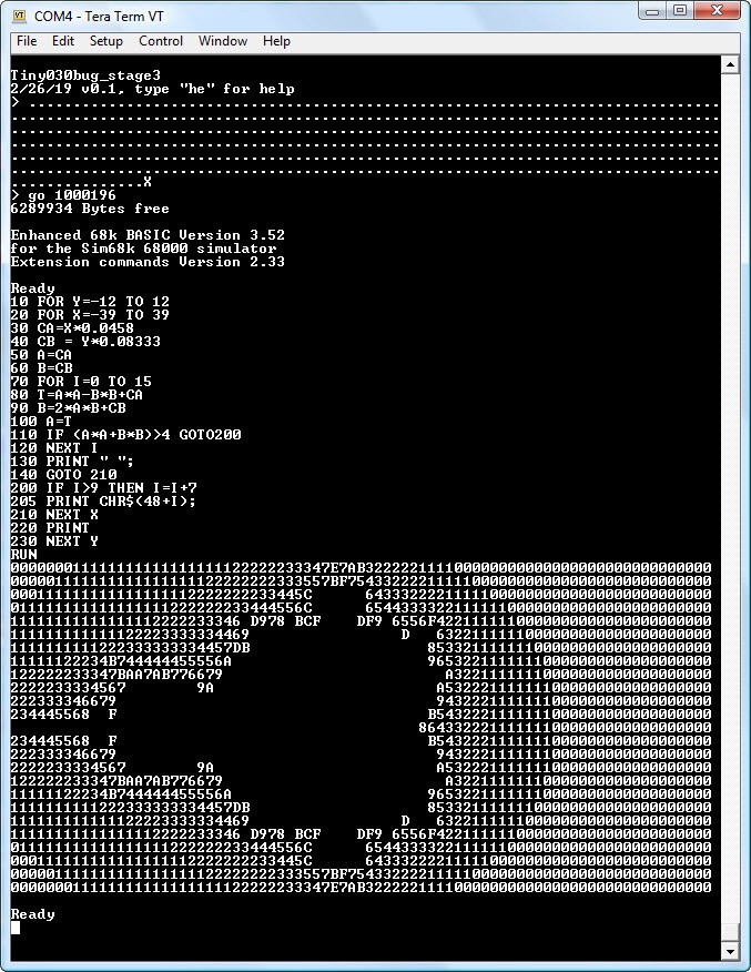
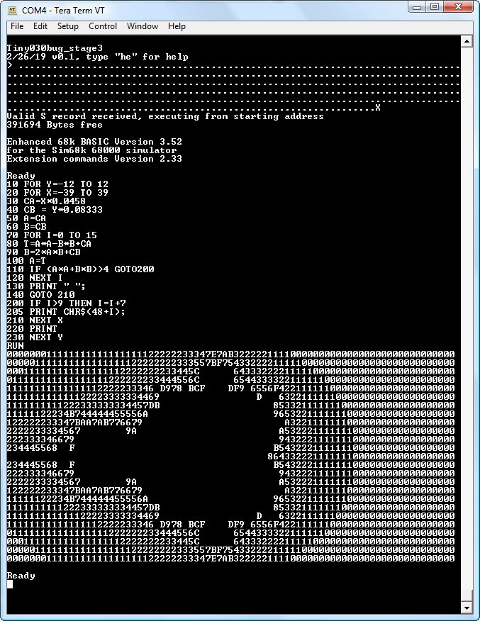
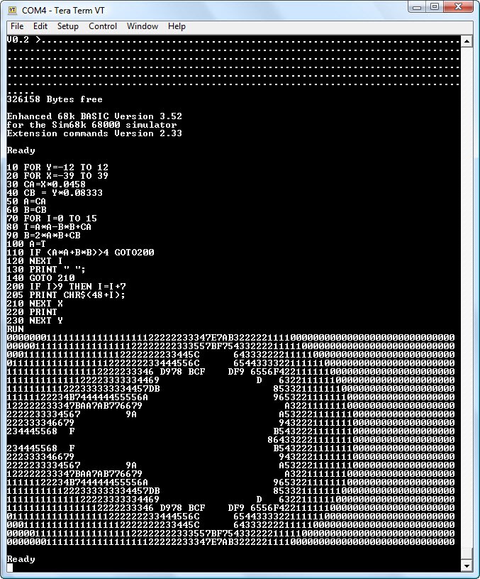
EhBASIC is relocated to 0x1000000 and allocated 6 meg of RAM. I measure the time it takes to run the ASCII mandelbrot at 27 seconds. Compare that to 45 seconds running in 8-bit RAM of stage 3. The improvement of 32-bit memory over the 8-bit memory is not as great as I would expected. I believe one reason is because the 8-bit RAM is running at zero wait state while 32-bit memory has 2 wait states for the slower DRAM circuitry.![]()
-
Stage 4, Adding 16-meg DRAM
03/02/2019 at 13:29 • 0 comments![]()
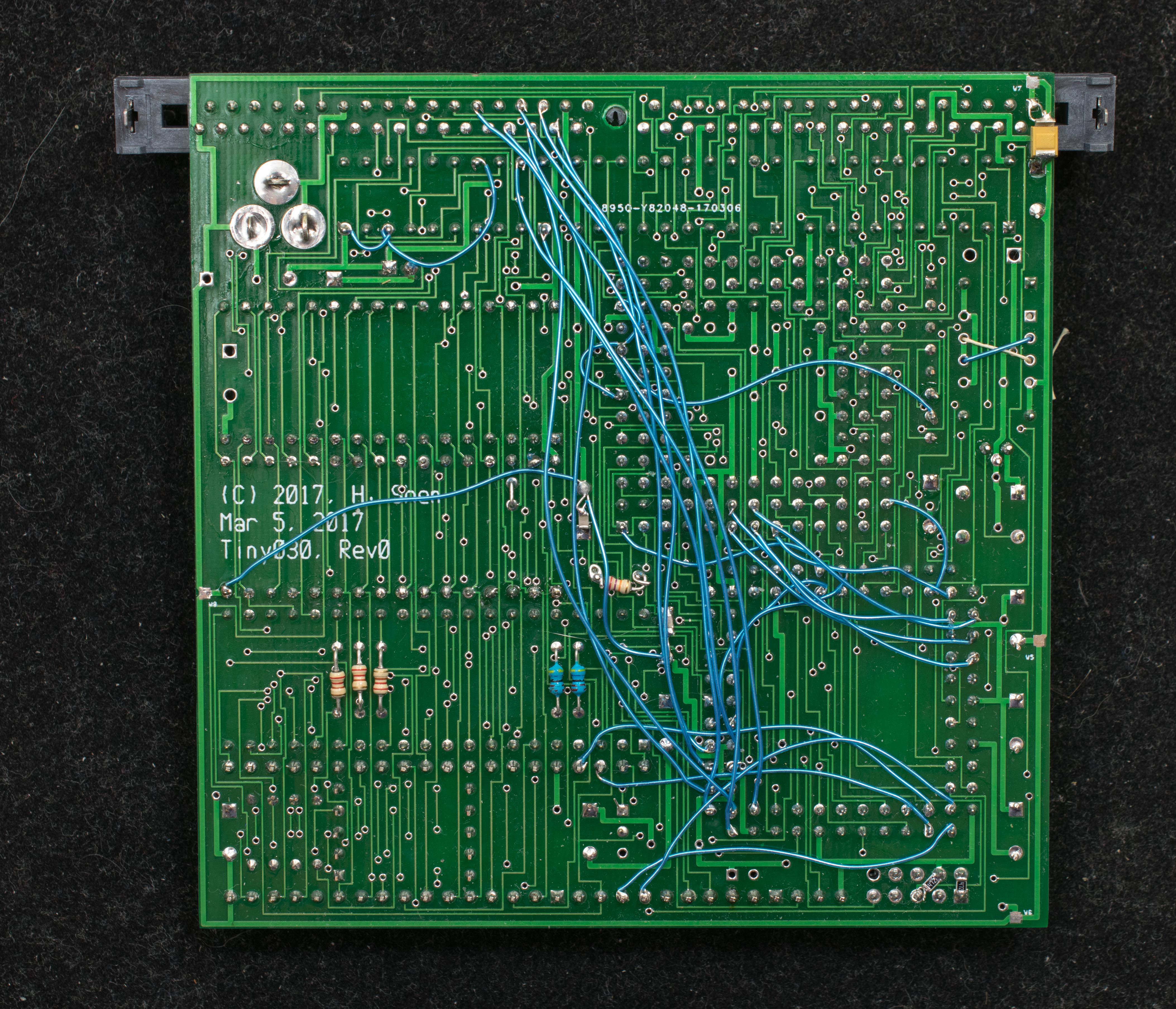
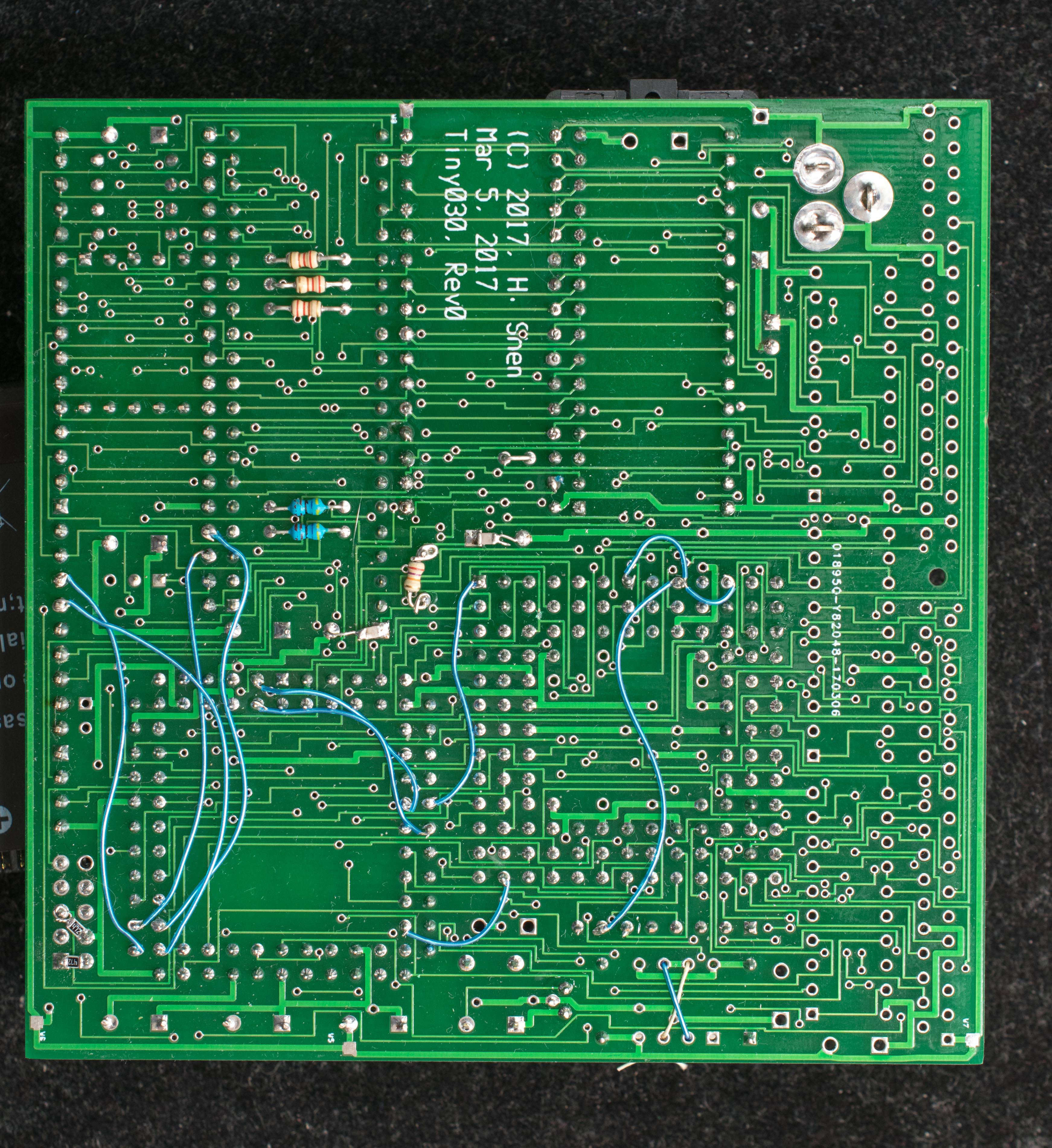
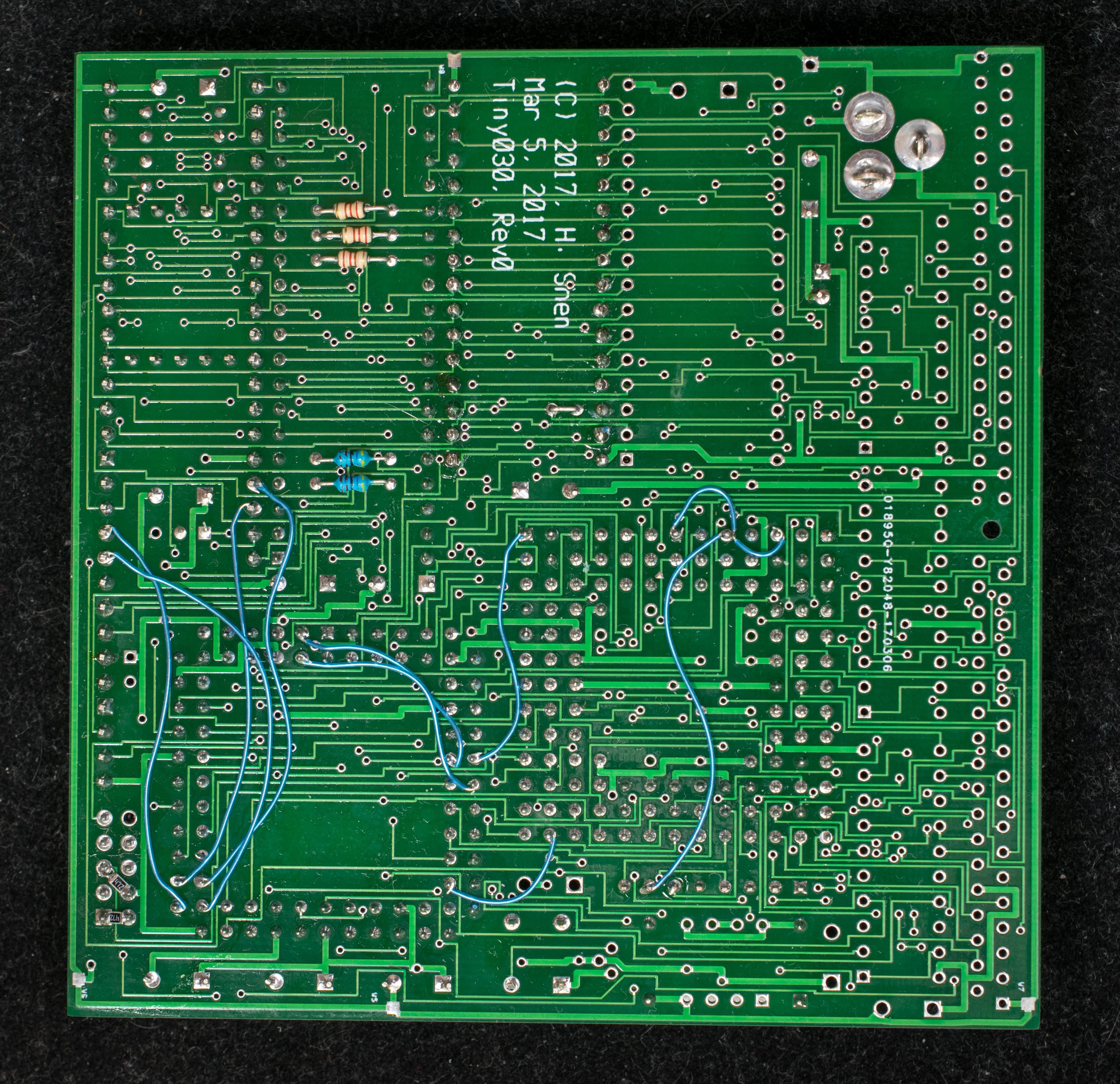
Stage 4 hardware construction is manual intensive. Installing U6-U8 (74HCT240) and socket for 16meg SIMM72 memory are straightforward, but there are many DRAM-related connections that are not hooked up in pc board. Here is a list of connections that need to be manually wired:
Signal CPLD pin 68030 pin A21 34 A8 A22 35 B7 A23 36 A7 A24 37 A6 A25 39 B6 Signal CPLD pin SIMM72 pin nRAS 76 44 nCAS0 81 40 nCAS1 80 43 nCAS2 79 41 nCAS3 77 42 nSIMMWE 73 47 Signal CPLD pin U7 (74HCT240) pin nENCASA 75 1 nENRASA 74 19 Signal U7 (74HCT240) pin U7 (74HCT240) pin floating
Input8 Ground (10) floating
input17 Ground (10) ![]()
The CPLD equations will need the DRAM controller and refresh logic added. The refresh is CAS-before-RAS driven by a timer and logic that delays the assertion of 68030 DSACKx signals until CAS-before-RAS refresh cycle is completed. This hidden refresh operation occurs once every 128 clock invisible to the 68030. The DRAM controller is a digital delay tap clocked on rising as well as falling edge of clock. Two wait states are needed to access the DRAM. The design can be improved by using 74157 mulitiplexer to reduce the wait state to 1.
The 16-meg DRAM memory map is from 0x1000000-0x1FFFFFF.
-
Stage 3 Software
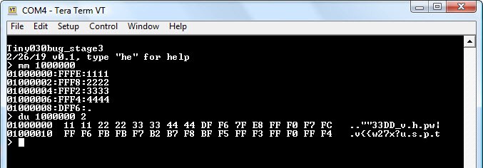
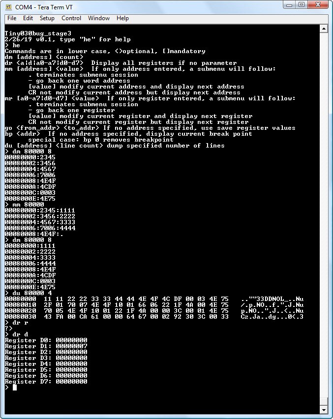
02/28/2019 at 13:29 • 0 commentsTiny030 at stage 3 is a fully functional computer. I have developed a simple ROM monitor previously for 680x0 board so with small modification, it is suitable as Tiny030 ROM monitor. As a monitor, it has the basic functions of display/modify memory, display/modify registers, load S-records, and execute program. It communicates with the terminal program at 38400-N-8-1, no handshake. It also perform basic I/O using TRAP15 calls compatible with EASy68K simulator, so a program can be simulated first with EASySIM and then load & execute in Tiny030 without modifications. A 'he' command display the menu as follow:
![]()
As a state-of-health indicator, the 7-segment LED displays the various state of the monitor software as it boots up and a rotating LED segments during idle state.
Since the address map of the RAM has changed since Stage 2, the memory diagnostic need to relocate to the new base address. It is loaded & executed with the Tiny030 monitor.
![]()
The memory diagnostic passes, so now I'm ready to load the EhBASIC which also need to be modified slightly to accommodate the different memory map between stage 2 and stage 3 hardware. Once EhBASIC is loaded, I load up the mandelbrot program and run it.
![]()
So Stage 3 Tiny030 has a functioning ROM monitor. It passes memory diagnostic, and it can run real applications like EhBASIC. We are ready to go to Stage 4.
-
Stage 3, 68030 with EPROM, RAM, and Dual UART
02/27/2019 at 16:22 • 0 commentsThe dual channel serial device, 68681 and EPROM are added in stage 3. It would be very desirable to build on stage 2 serial bootstrap feature to test the hardware added in stage 3. Alas, the board was not designed with that in mind and the amount of rewiring is too onerous. The revised Tiny030 will have jumper configuration that preserves the serial bootstrap function as more devices are added. This would enhance the board testing capability and help with development of the permanent EPROM bootstrap software. With current hardware it is easiest to just dismantle the stage 2 hardware and add the 68681 and EPROM and get them working. All the efforts in stage 2 are not lost, however. We've found out that RAM/68030/CPLD are working correctly in stage 2, so if problems are encountered in stage 3, we can concentrate our efforts on the hardware that are added, i.e., EPROM and 68681.
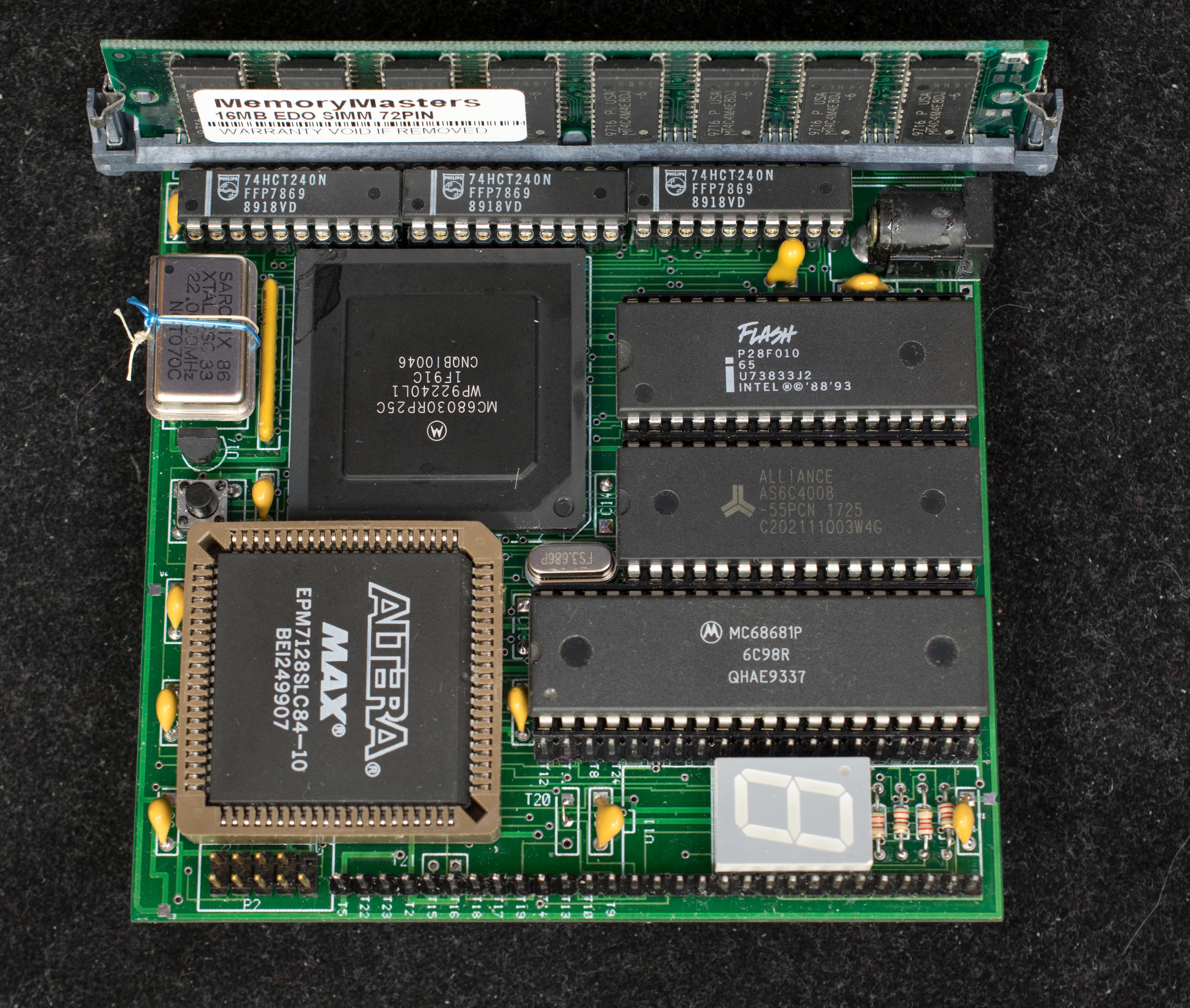
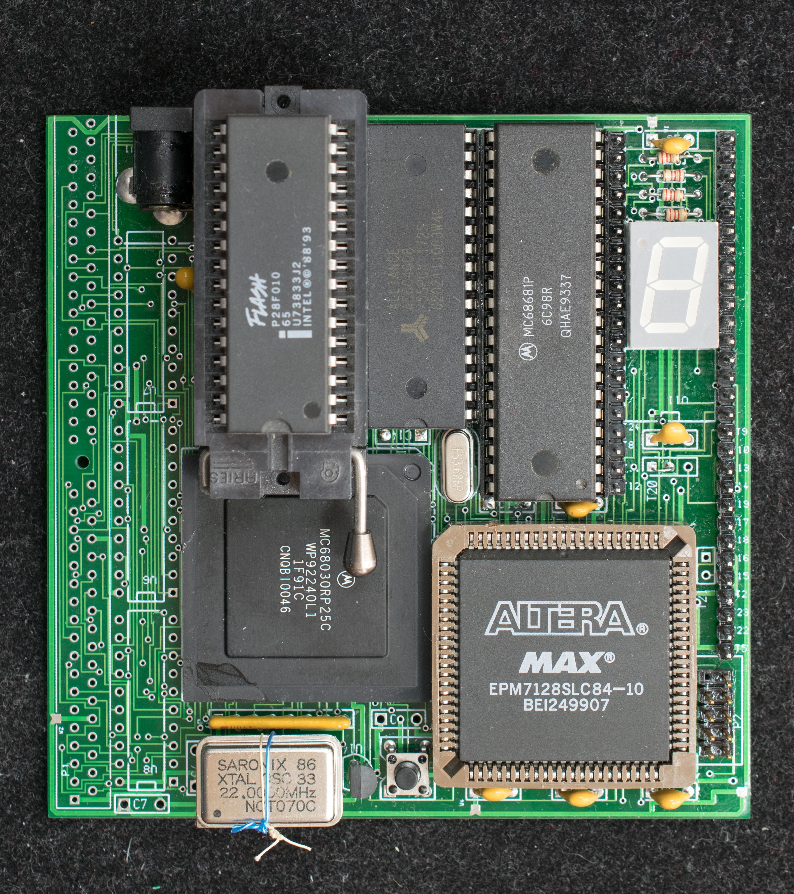
Picture below shows the stage 3 hardware configuration. The EPROM and 68681 sockets are added to the pc board. A zero-insertion-force socket is installed in EPROM's location to facilitate changing out EPROM. A 3.6864MHz crystal is added as baud rate generator for 68681. a 27K resistor is added across the crystal oscillator to bias it for oscillation. I use this opportunity to install the voltage supervisor and change the CPU clock to 22MHz.
![]()
![]()
The stage 3 CPLD equations are revised significantly. The serial bootstrap function is no longer required; the EPROM is added to the memory map. The chip select and interrupt signals of 68681 are added. This is now the memory map of stage 3 Tiny030
- EPROM 0x0-0x7FFFF
- RAM 0x80000-0xFFFFF
- 68681 0x100000-0x17FFFF
- Refer to 68681 data sheet for register mapping
Stage 3 hardware is powered up and CPLD updated. It is now ready for firmware and software.
-
Stage 2, Running Software on the minimal 68030 computer
02/25/2019 at 01:50 • 0 commentsThe minimal 68030 computer has 512K of RAM and a simple serial port. Here is the memory map of stage 2 68030 computer:
- RAM 0x0-0x7FFFF
- Serial port transmit/receive: 0xFFFFF000
- Serial port status 0xFFFFF001
- Bit 0 is TxEmpty, transmit buffer empty when high
- Bit 1 is RxRdy, receive data ready when high
A very simple program to output 'hello world' on console looks like this:
    org 0
    dc.l $80000        ;define stack
    dc.l start
start:
    lea signon,a0        ;point to sign on message
chktxempty:
    btst.b #0,$FFFFF001    ;test for transmit buffer empty
    beq chktxempty
    move.b (a0)+,$FFFFF000    ;write next character to console
    bne chktxempty            ;until null terminator
    bra *                    ;spin forever here
signon: dc.b $a,$d,'Hello World!!!!!',0
    end
The assembler for this code is EASy68K. The EASy68K tool chain has an utility, EASyBIN, that can convert S-record to binary format and fills the file to specified length which is 0xFF in this case. This way the program will start running as soon as file loading is completed.![]()
OK, now that 68030 can receive a 255-byte program and execute it, let us write a 255-byte S-record loader. This simple loader will load a S-record file and start program execution from 0x400 when loading is done. To test this loader, I modified the above 'hello world' program so it starts from 0x400. First load the S-record loader, and then load helloworld_400.
![]()
That works, so I will now load and execute a memory diagnostic that checks the 1/2 meg RAM from 0x1000 to 0x7FFFF. The program and stack reside below 0x1000 so that part of the memory can't be checked with the diagnostic. First load the S-record loader, then load tstmem.s68![]()
That works well, now I'm ready to load a real application, Lee Davison's EhBASIC for 68000. This program is available for download from EASy68K website. The source code is modified slightly to accommodate the simple serial port. Once EhBASIC is loaded and running, I will load a ASCII mandelbrot program and run it under EhBASIC.![]()
This collection of software demonstrate the stage 2 hardware is working properly and we are ready to move on to stage 3. -
Stage 2, A minimal 68030 computer
02/21/2019 at 16:15 • 0 commentsOnce the CPLD is checked out and working, we are ready for stage 2. Stage 2 is to assemble a bare minimum 68030 computer that contains 68030, RAM, CPLD and an oscillator.
![]()
There are a number of manual wires need to be done at the back of the board:- Pull up nCIIN, nCBACK, nSTERM to pin 7 of SIP resistor pack R9
- Connect Address 7 from pin 31 of CPLD to pin B13 of 68030
- Cut the trace between pin A1 of 68030 to pin C3. This isolates nBUSREQ from nBGACK of 68030
- Connect pin 20 of CPLD to nBUSREQ (pin A1) of 68030
- Connect pin 21 of CPLD to pin 83 (nAS) of CPLD
- Connect pin 22 of CPLD to pin 84(R/W) of CPLD
- Connect pin 54 of CPLD to test point T13
- Connect pin 55 of CPLD to test point T14
- Connect pin 56 of CPLD to test point T8
- Connect pin 57 of CPLD to test point T24
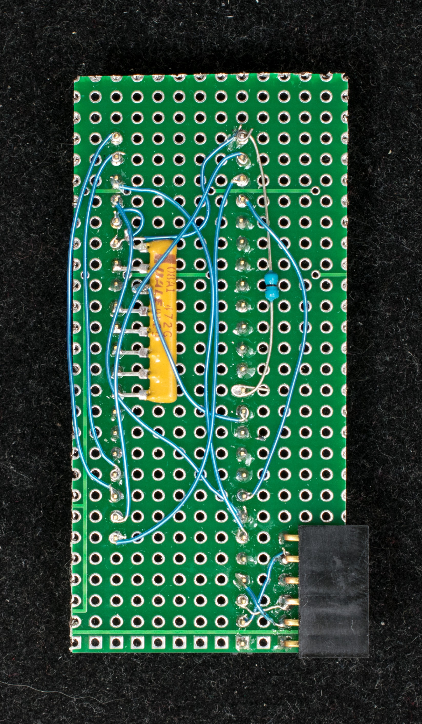
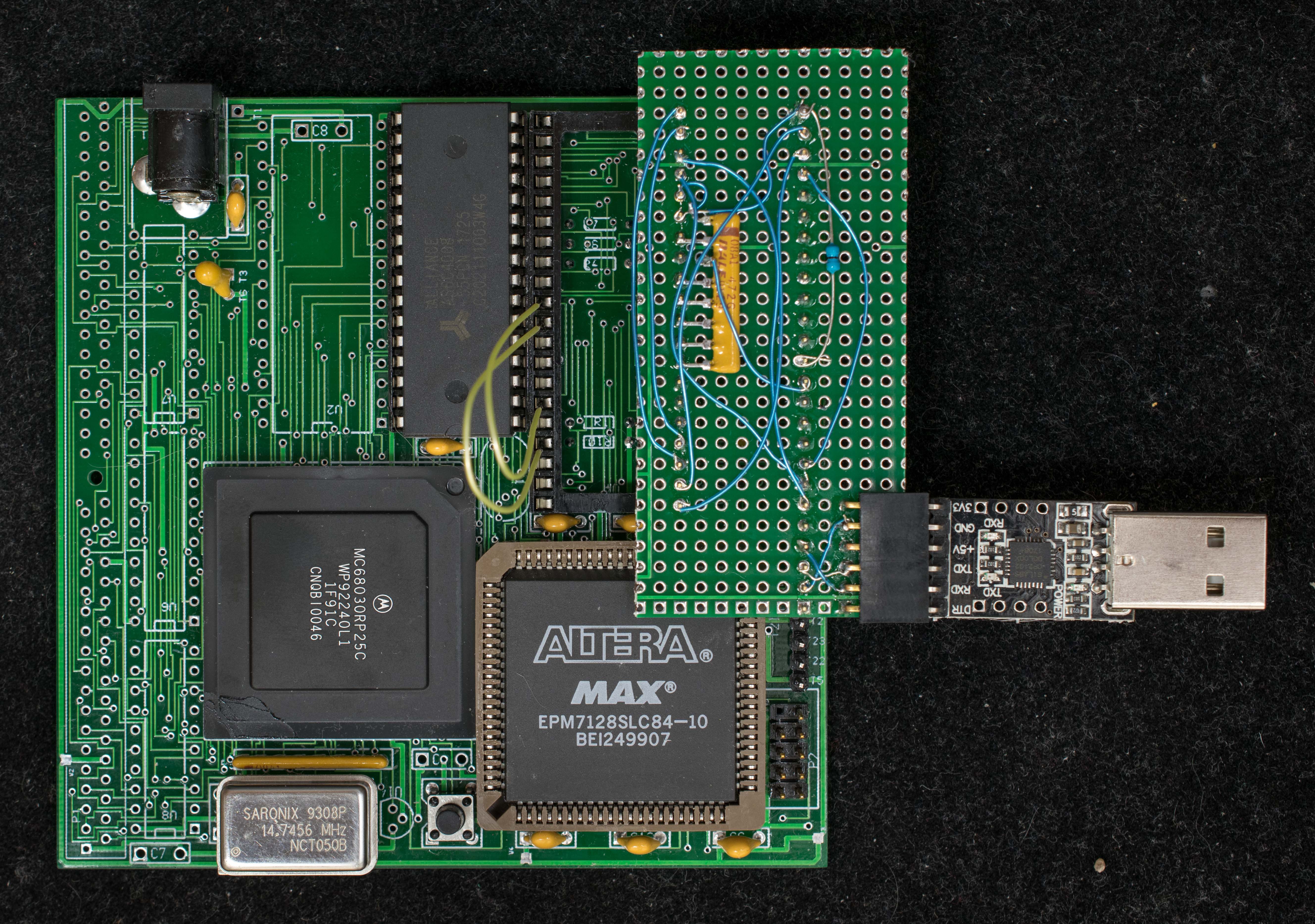
![]() A prototype board with additional manual wires need to plug into the expansion headers, U11 to enable the serial bootstrap function
A prototype board with additional manual wires need to plug into the expansion headers, U11 to enable the serial bootstrap function![]()
Here is the board that's ready to power up.
![]()
The USB-to-serial adapter connects to terminal emulation (I use TeraTerm) program at 115200-N-8-1. Programmed in the CPLD is a simple serial port and DMA circuitry controlled by a state machine. At power up the CPLD state machine generates a bus request to 68030, then the state machine takes control of the 68030 address and data bus and waits for serial data input. Every data received is DMA to memory starting from location 0x0 until 255 bytes of data is received. At that point the state machine relinquishes the bus and 68030 starts program execution from 0x0 like a normal power-on reset operation. The small 255-byte program is typically a simple file loader that load more sophisticated application programs. This is the mechanism by which the minimal 68030 computer can be loaded with diagnostic software to further test the board and to develop application software.
A reasonable question can be ask whether this stage is consider a "baby step" due to the many manual wires where mistakes can easily be made. That's a good point for this particular version of pc board, but I also want to use this experience to develop a revised pc board where stage 2 can be done without too much manual wiring.
This is the CPLD file for stage 2 68030 computer
-
First Stage, Assemble and Test the CPLD
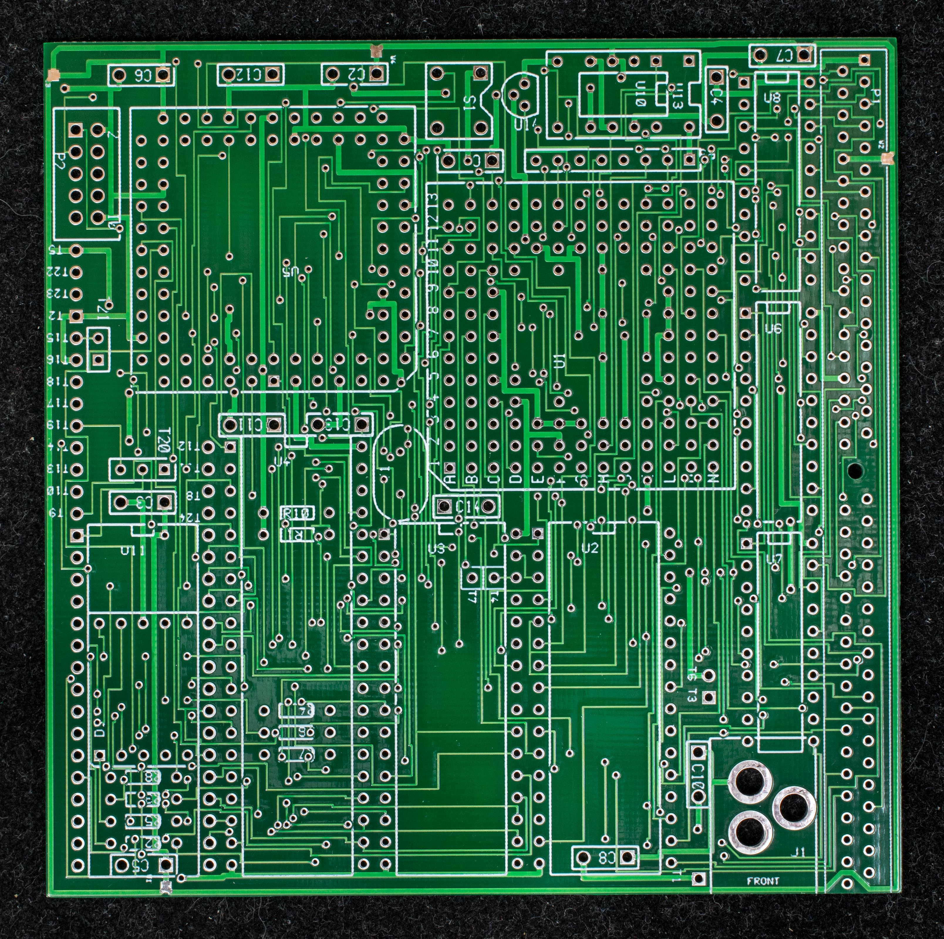
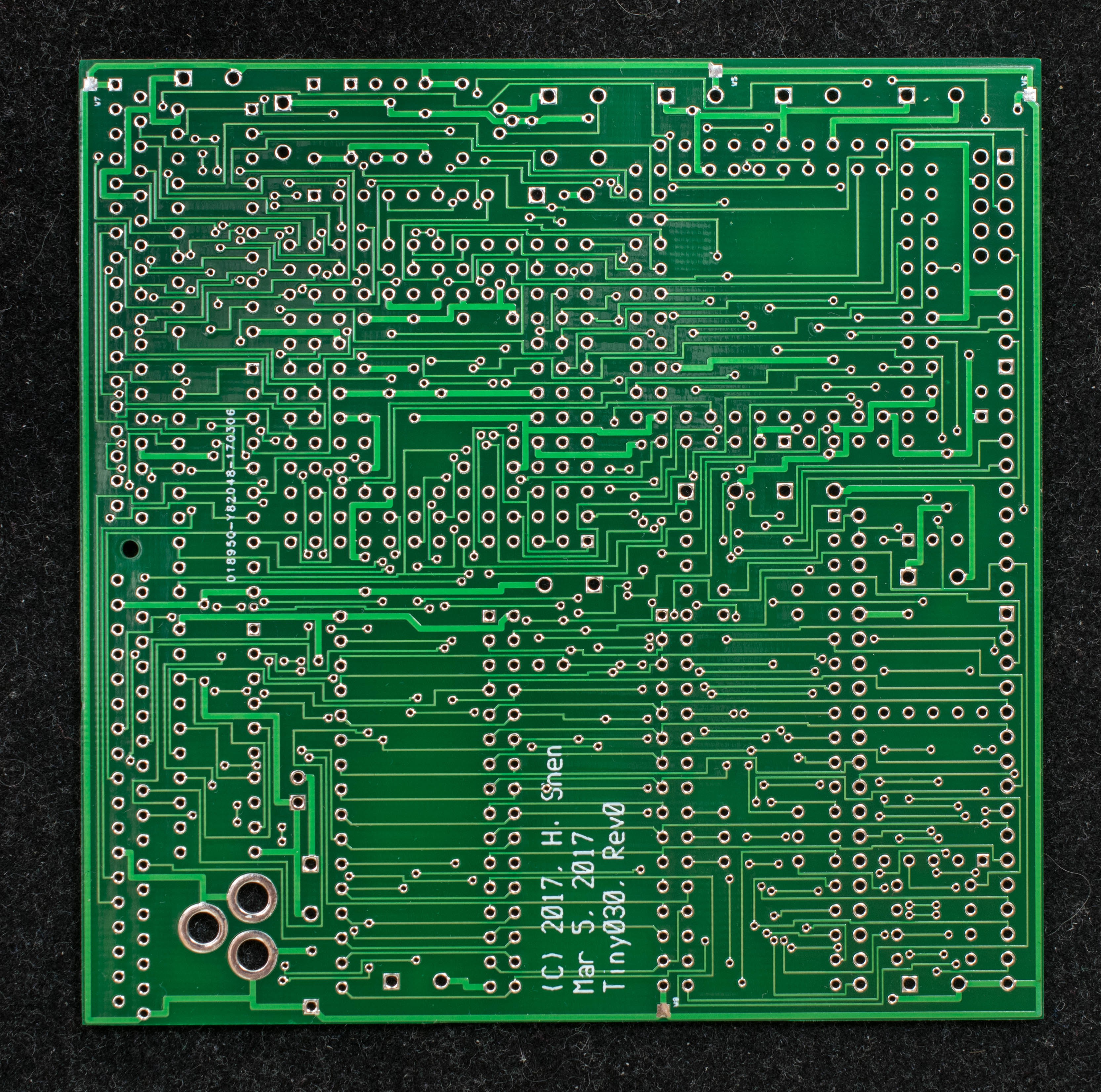
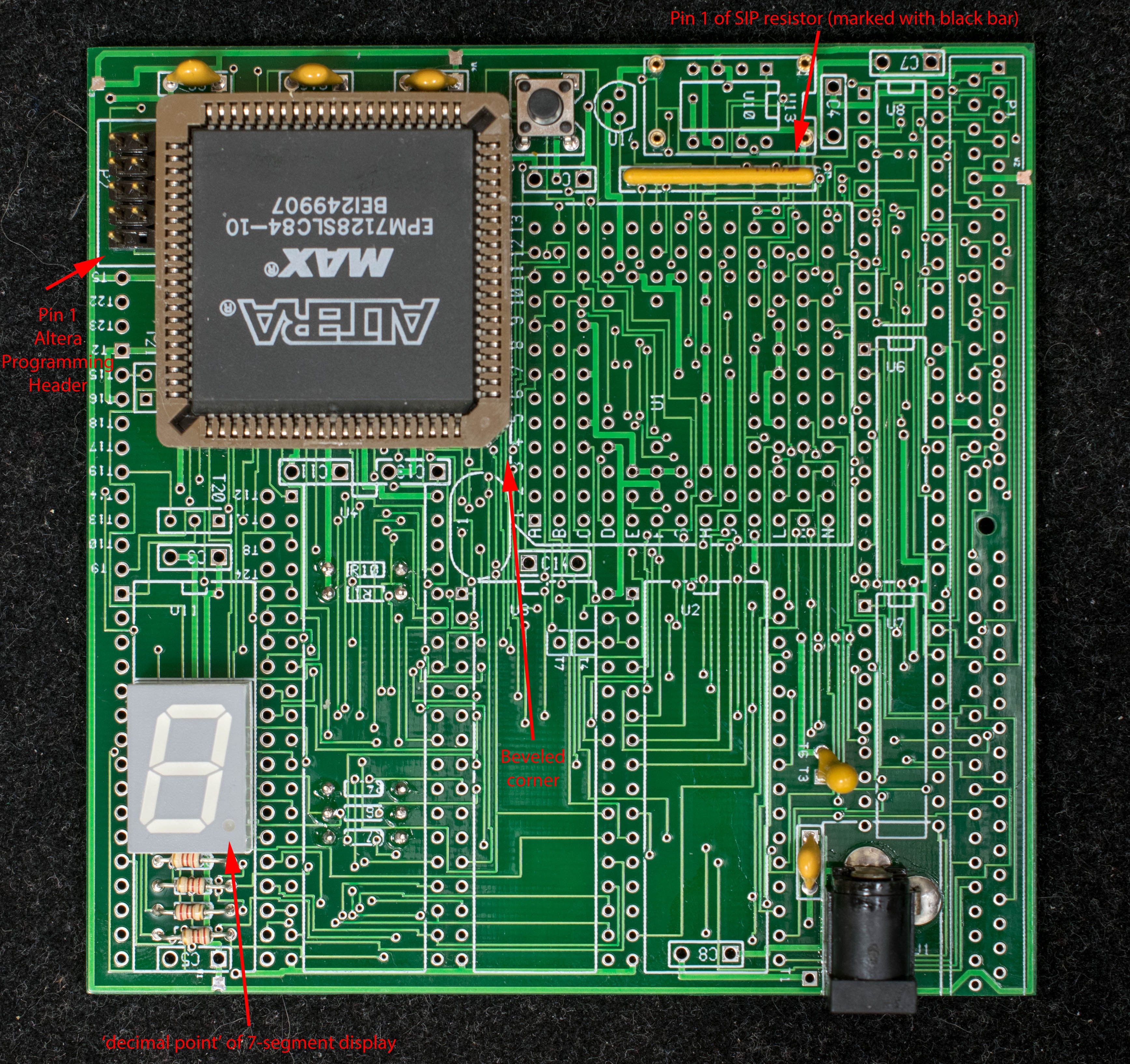
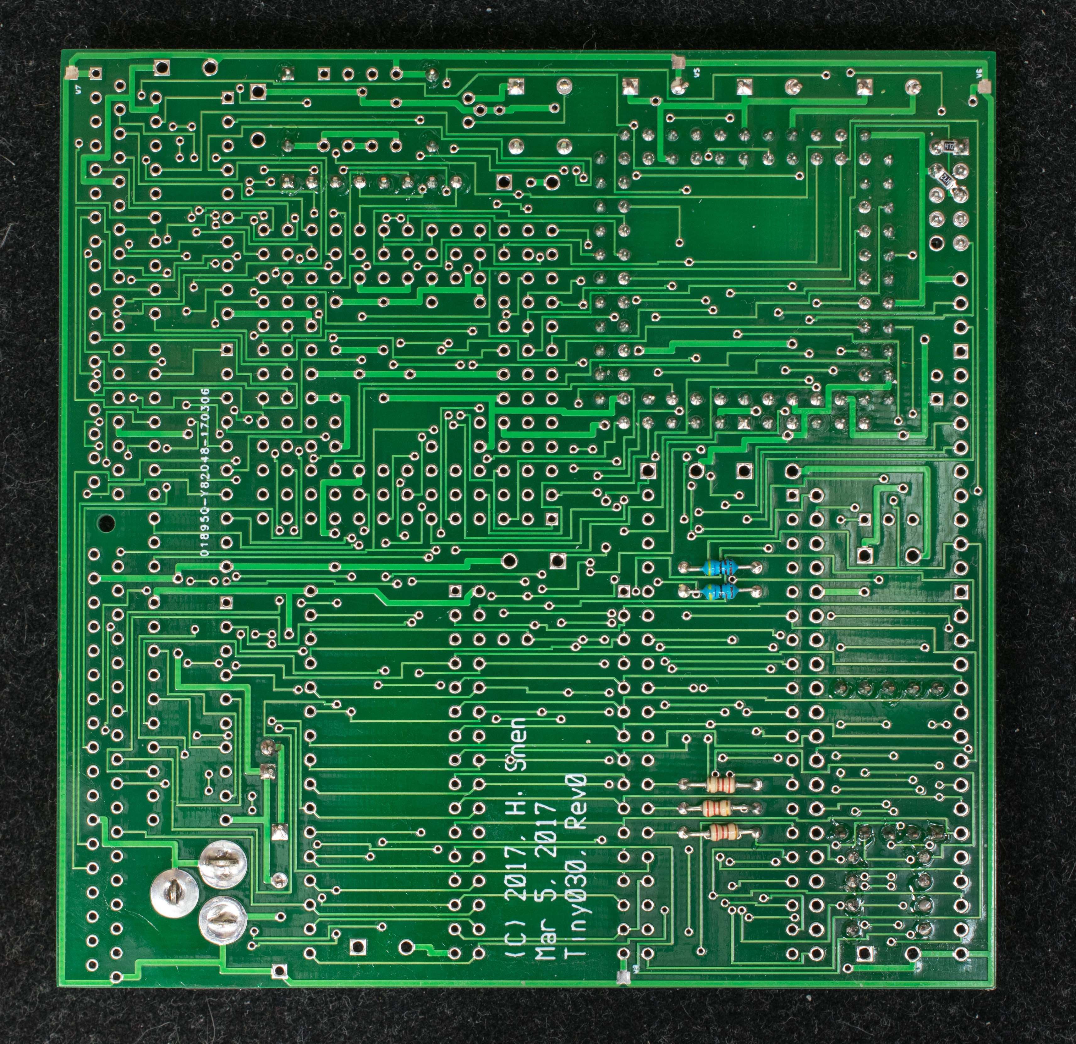
02/21/2019 at 16:13 • 1 commentStart off with a blank Tiny030 pc board:
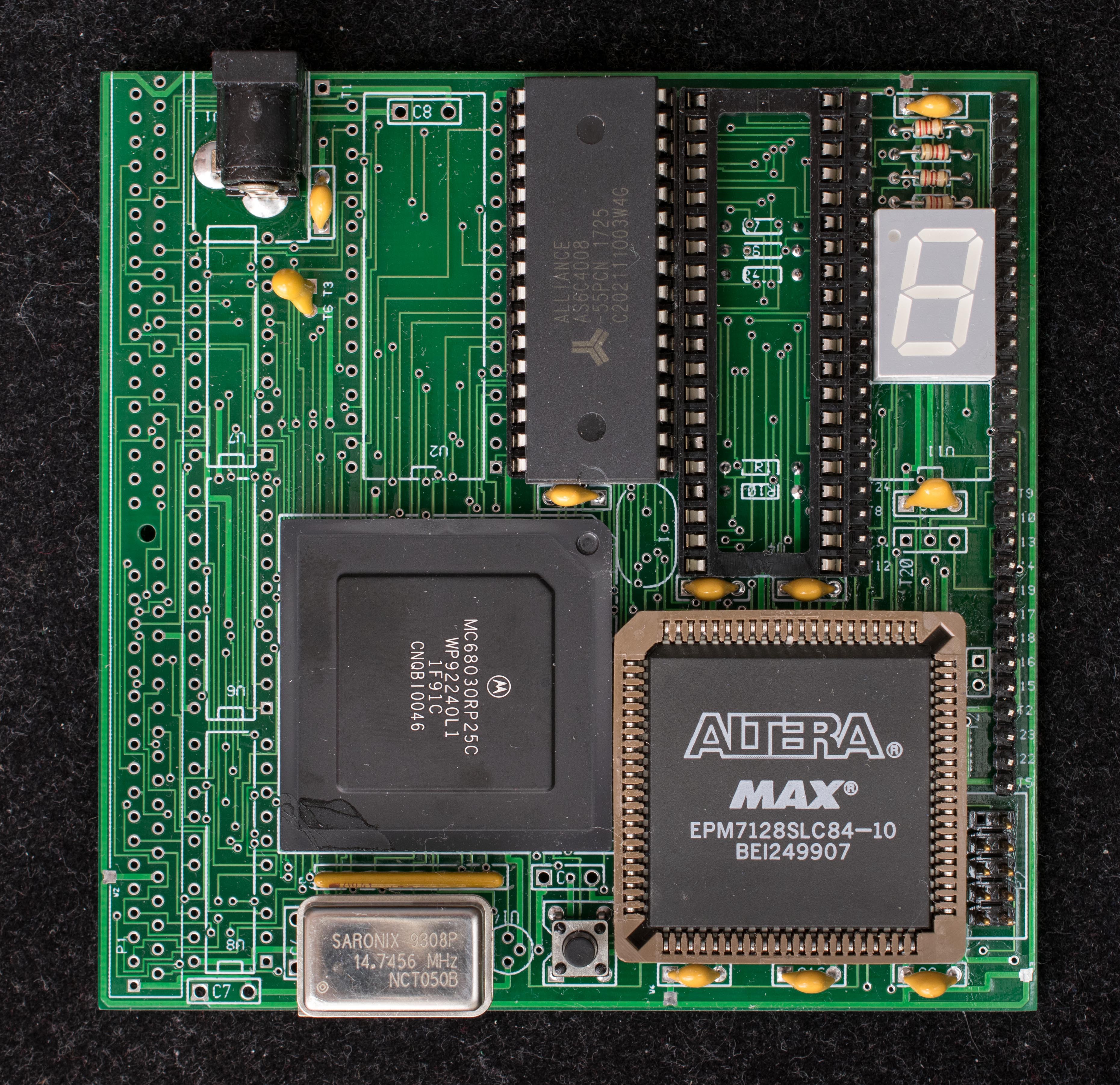
![]()
![]()
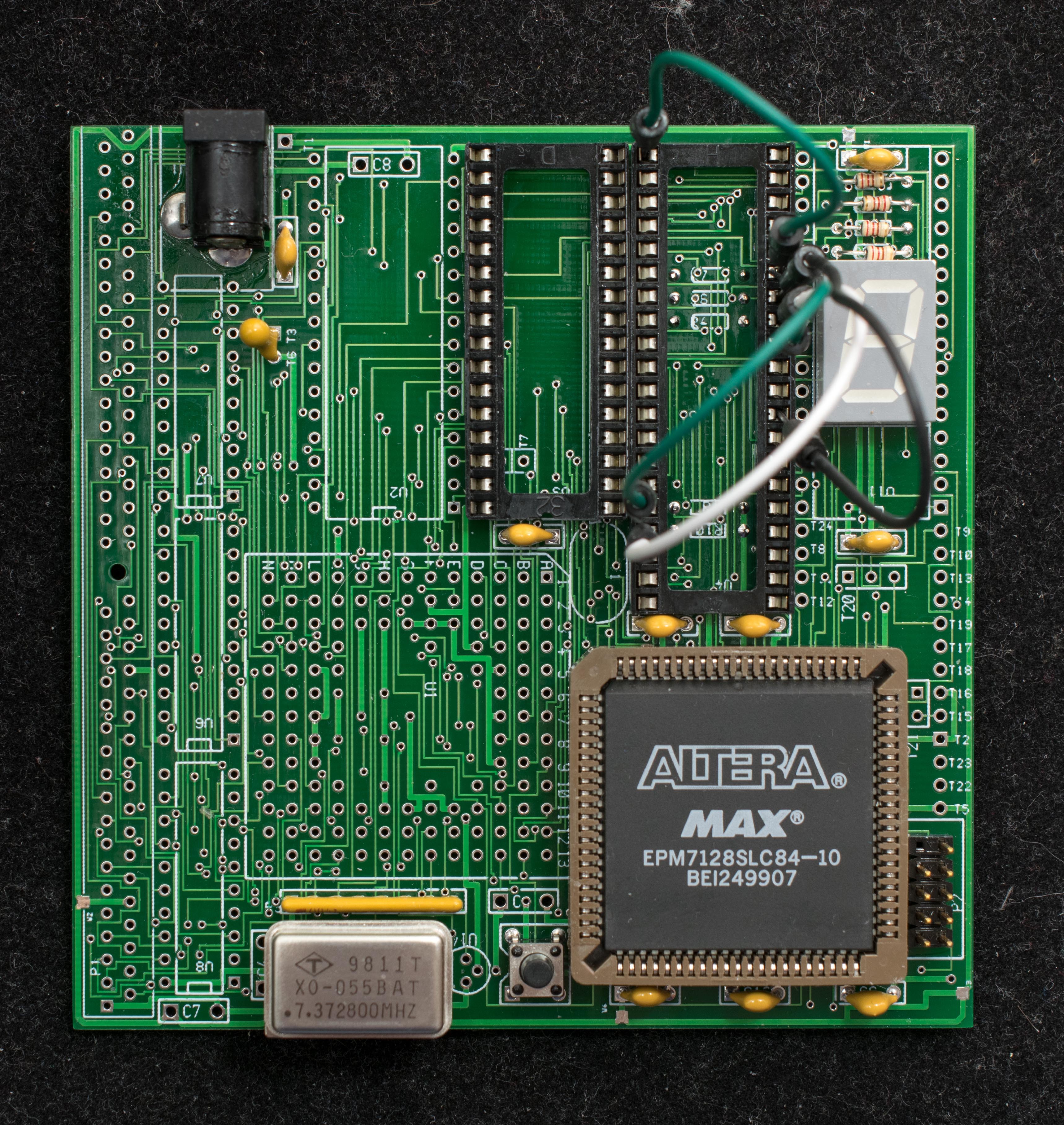
The first stage is to assemble and test the CPLD by driving a few LEDs. The CPLD is Altera EPM7128SLC84 hosted in a through-hole 84-pin PLCC socket.
![]()
![]()
Add the 68681 40-pin socket because jumpers are needed to connect CPLD output to 7-segment display. Populate the EPM7128SLC84 as shown and insert 4 jumpers from the 68681 socket as follow:
- pin 12 to pin 35
- pin 13 to pin 37
- pin 14 to pin 9
- pin 15 to pin 21
This connect 4 currently unused CPLD outputs to 4 of the 7-segment display. Also populate the oscillator. Here is the Altera CPLD programming file.
![]()
 Plasmode



 A prototype board with additional manual wires need to plug into the expansion headers, U11 to enable the serial bootstrap function