 Md. Khairul Alam
-
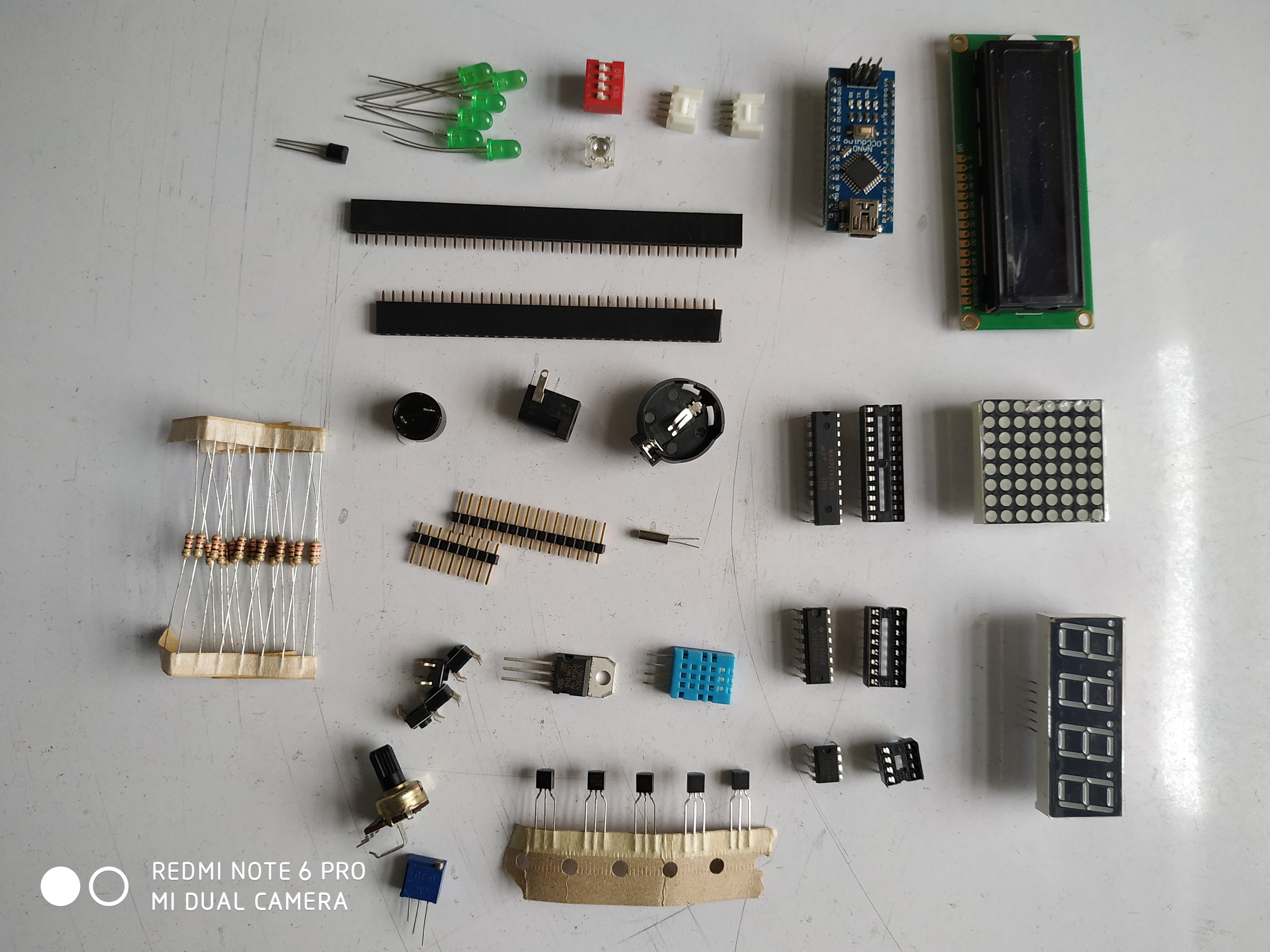
1Collecting the Components
The first step is to collect all the components mentioned in the component list. All the components are very common. So you can find the components in your local parts store. You can also buy the components from aliexpress.com or gearbest.com.
![]()
-
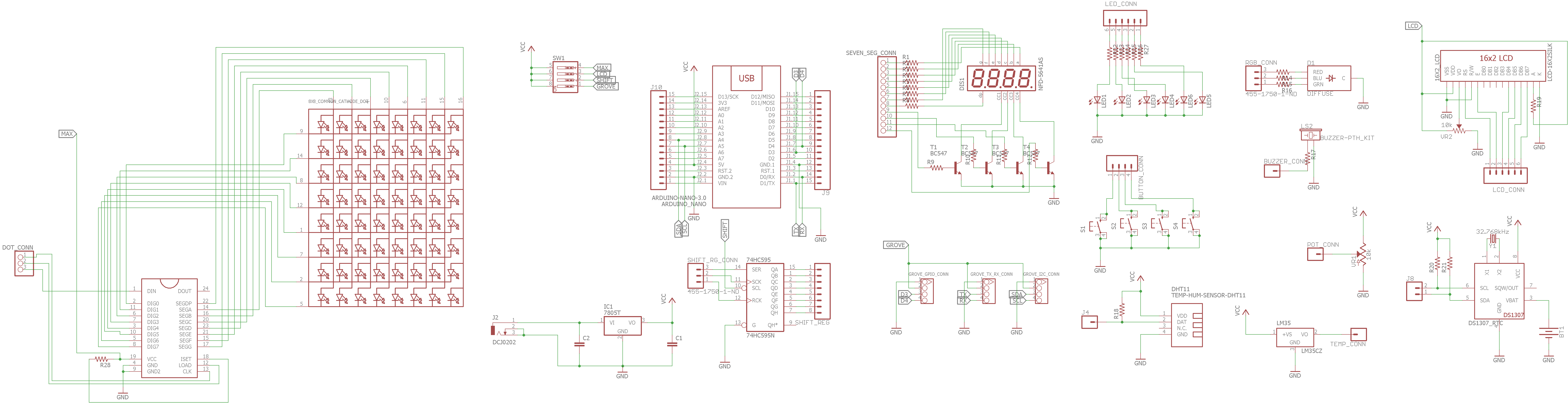
2Designing the Schematic
This is the most important step of making the kit. The complete circuit and board layout were designed using Eagle cad. I make the schematic part by part so that it can be easily understandable and you can modify it easily according to your requirement.
![]()
The Eagle source file is attached in the file section. You can download the source from that section.
-
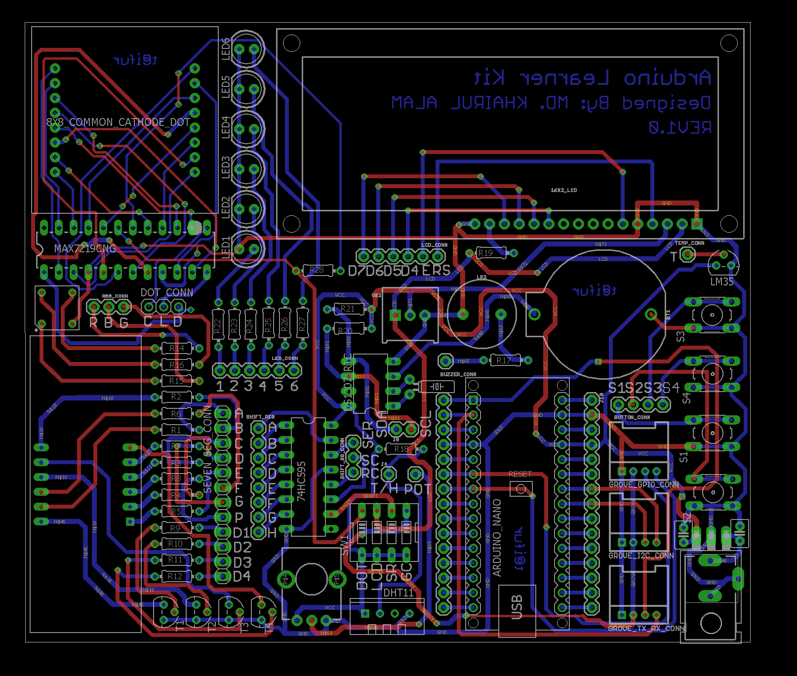
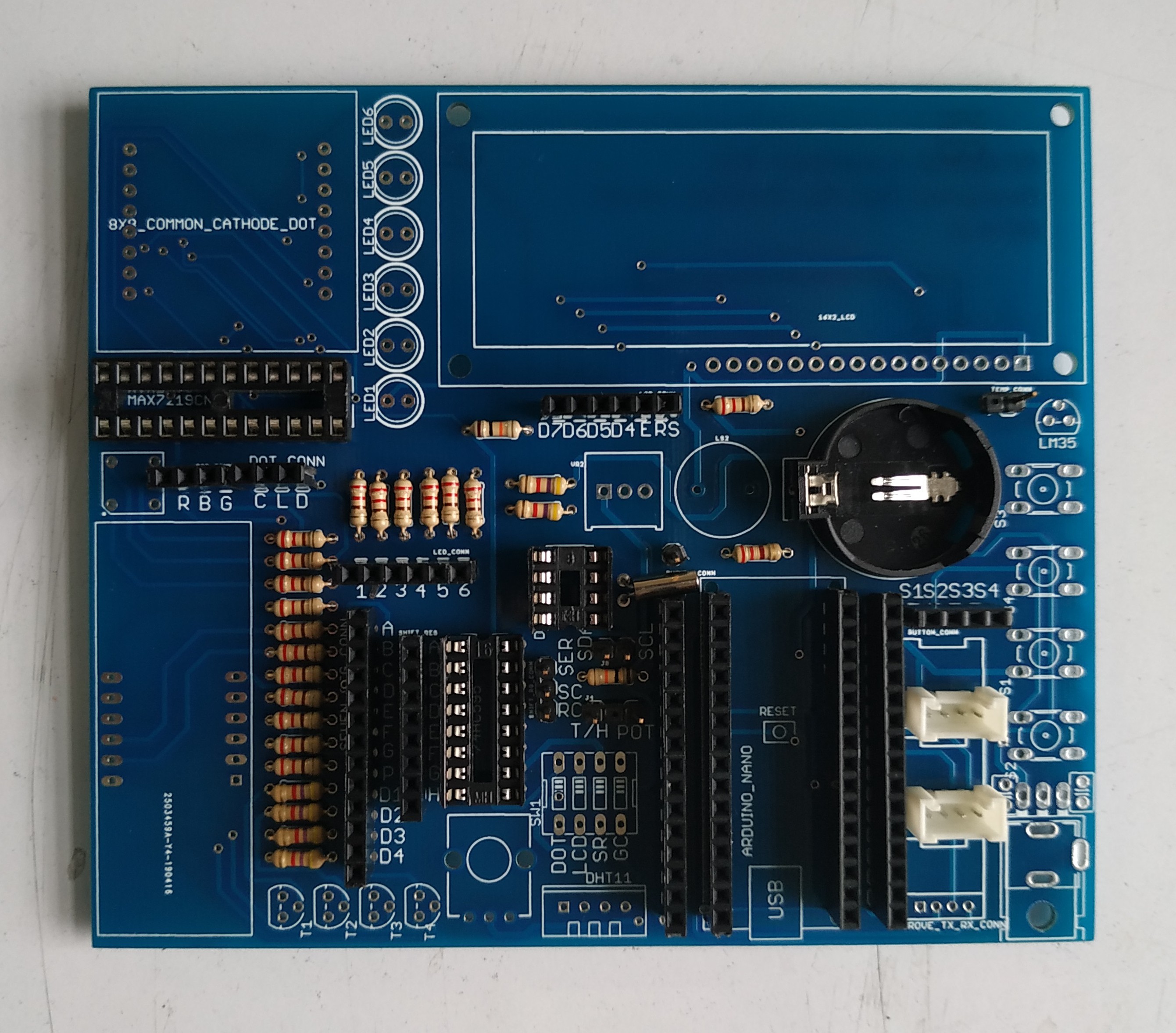
3Designing PCB Layout
If you want to make your design more appealing, then PCBs are the next step. With the help of PCBs, we can avoid common problems like noise, distortion, imperfect contact, etc. Moreover, if you want to go commercial with your design, you have to use a proper circuit board.
But, many people, especially beginners, will find it difficult to design circuit boards as they feel it as a tedious job and requires extreme knowledge in circuit board design. Designing printed circuit boards is actually simple (yes, it does need some practice and efforts).
![]()
Note that the Schematic's job is only to define the parts and the connections between them. Only in Board layout does it matter where the parts physically go. On Schematics, parts are laid out where they make sense electrically, on Boards, they are laid out where they physically make sense, thus a resistor that is right next to a part in the Schematic may end up as far away from that part as possible in the Board.
Typically, when you lay out a board, you first place the parts that have set locations that they need to go, like connectors. Then, group up all parts that logically make sense together, and move these clusters so that they create the smallest amount of crossed unrouted lines. From that point, expand those clusters, moving all of the parts far enough apart that they don't break any design rules and have a minimum of unrouted traces crossing.
One thing with printed circuit boards is that they have two sides. However, you typically pay per layer that you use, and if you are making this board at home, you might only be able to reliably make one-sided boards. Due to the logistics of soldering through-hole parts, this means that we want to use the bottom of the PCB.Use the Mirror command and click on the surface-mount parts to switch them to the bottom layer. You may need to use the Rotate or Move command to correct the orientation of the parts. Once you have all of the parts laid out, run the Ratsnest command. Ratsnest recalculates the shortest path for all of the unrouted wires (airwires), which should clear up the clutter on the screen by a fair amount.
The Eagle source (.brd) file is attached in the file section. Download from that section.
-
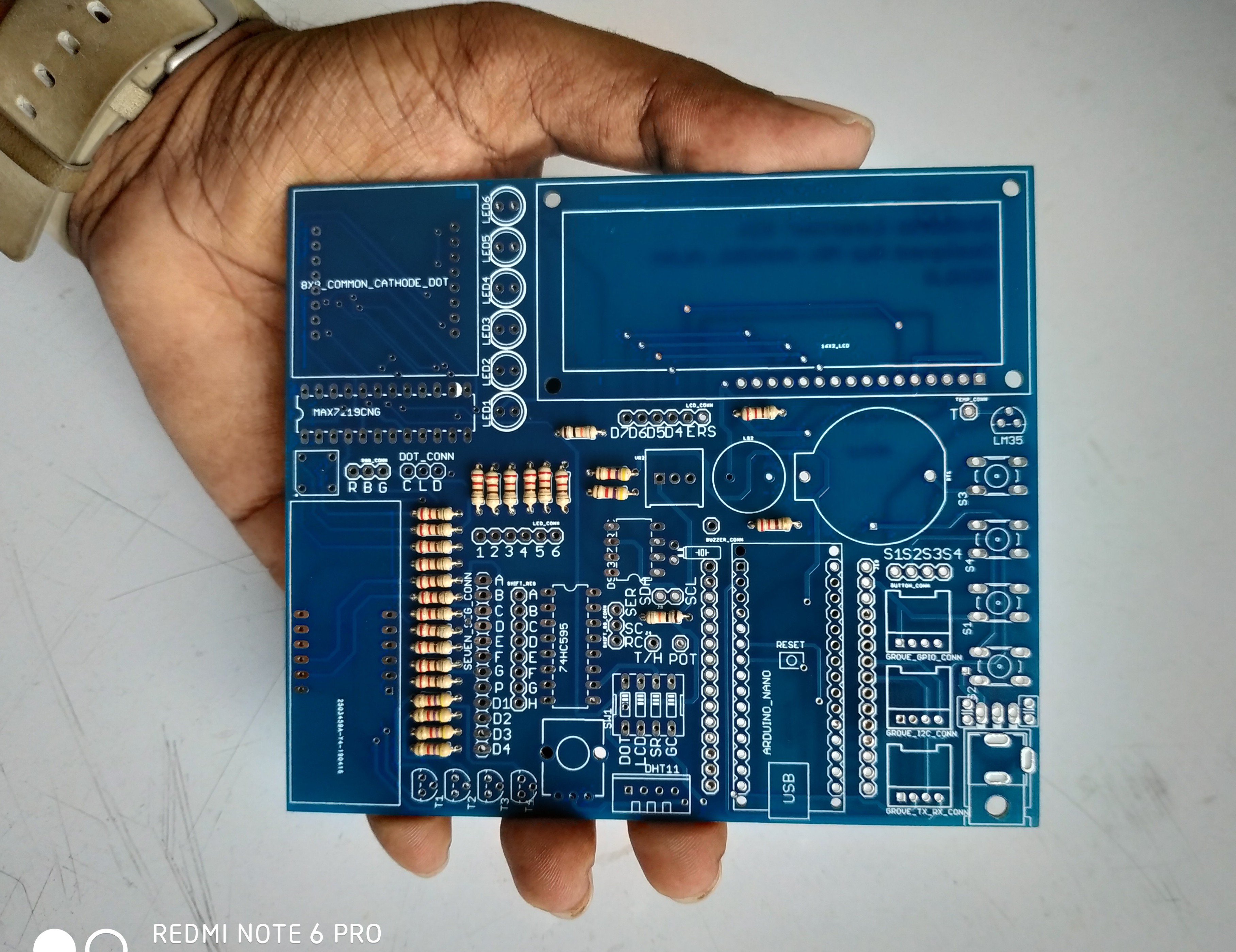
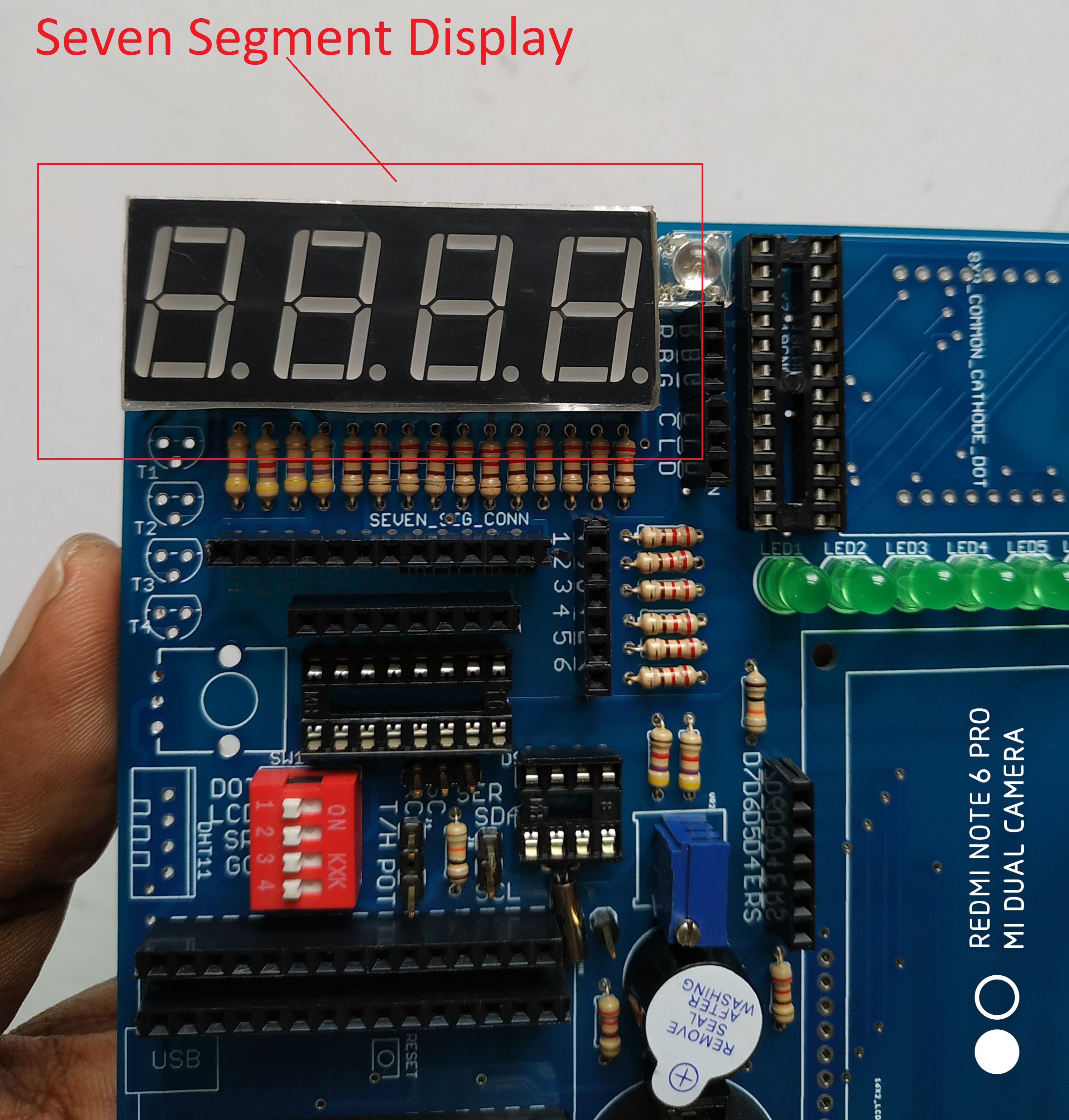
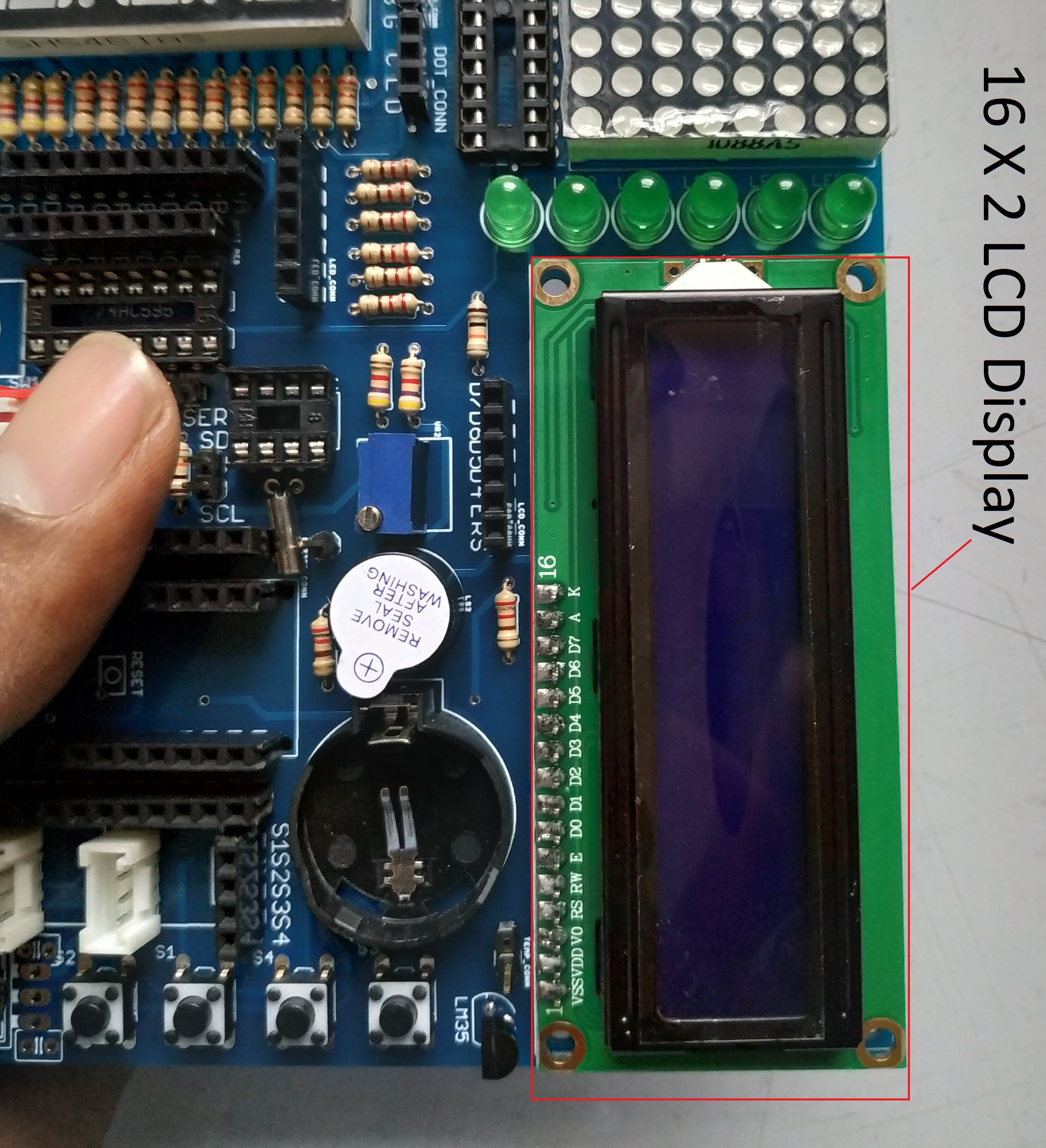
4Soldering the Components
After making the PCB you need to solder all the components in the PCB board. Soldering is one of the most fundamental skills needed to dabble in the world of electronics. The two go together like peas and carrots. And, although it is possible to learn about and build electronics without needing to pick up a soldering iron, you’ll soon discover that a whole new world is opened with this one simple skill. Soldering is the only permanent way to ‘fix’ components to a circuit. And basic soldering is easy. All you need is a soldering iron and some solder. When my dad taught me as a teenager, I remember picking it up quite fast.
![]()
Solder small parts first. Solder resistors, jumper leads, diodes and any other small parts before you solder larger parts like capacitors and transistors. This makes assembly much easier. Install sensitive components last. Install CMOS ICs, MOSFETs and other static sensitive components last to avoid damaging them during assembly of other parts.
![]()
In last stage, solder three big components (seven segment display, dot matrix display and the LCD display). First, I soldered seven segment display to the board because it is the smallest in size and less sensitive. Then I placed the dot matrix display. After soldering the dot matrix display I placed the last component, the LCD display to the board. Before placing the LCD to the board I first soldered male pin header to the LCD and then placed to the main PCB board. The soldering job is done with soldering of LCD.
![]()
![]()
Open Source Arduino Learner Kit
This is a hardware development board designed for Arduino beginners. Lots of IO devices are in-built in the board.
Discussions
Become a Hackaday.io Member
Create an account to leave a comment. Already have an account? Log In.