-
Online Javascript assembler/simulator
12/08/2019 at 19:13 • 0 commentsThe online assembler can now also simulate the Kobold K2 !
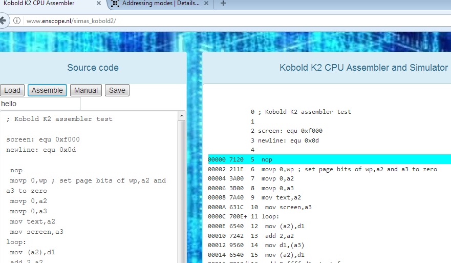
![]()
The picture shows the panel with the source code, and the panel with the assembled code, and the first line highlighted (click for bigger version).
You can run and singlestep. An integrated tiny disassembler shows the EA (effective address), the value at the effective address (or the immediate value VAL) just before executing the instruction.
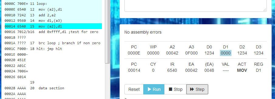
![]()
At the lower left, you see the highlighted instruction with opcode 0x6540 in the IR (instruction register), the effective address is 0x0042, and at that address is the value 0x0048. It also says that it will MOV that value to register D1.
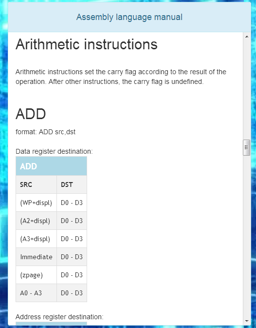
There is a new online instruction manual that shows all instructions and the addressing modes that are valid for them. When you activate the manual, it pops up at the side of the screen so you can still see and edit your program.
![]()
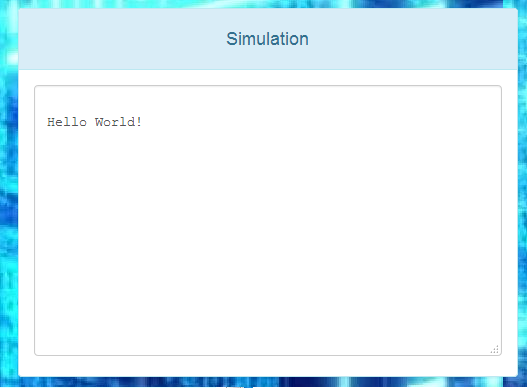
And of course, there is a window that shows the text output of the simulation:
![]()
Try it all LIVE, now near to you at Kobold K2 Assembler/Simulator !
A free beer if you are the first to write a K2 program that generates primes !
-
PCB's ordered
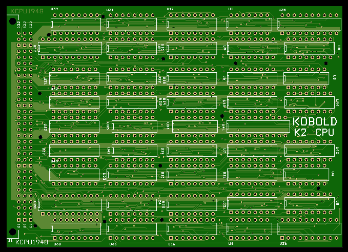
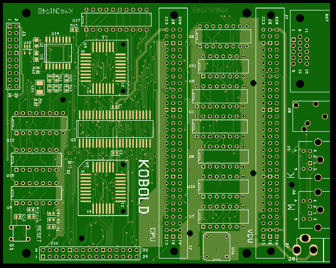
11/29/2019 at 21:17 • 0 commentsTwo PCB's are designed now:
- The CPU
- A mainboard for the CPU
The video part is not designed yet. The mainboard has a 96 pin connector (same as CPU) where the video PCB can be placed once it is ready.
Here comes the CPU impression from the PCB makers website:
![]()
And the mainboard:
![]()
The mainboard has:
- DIN41612 connector for CPU
- DIN41612 connector for Video card
- Two 8-bit wide PLCC Flash ROMs
- 256K x 16 SRAM
- 32 MByte serial SPI flash
- clock circuits
- address decoding
- some I/O
- connector for Raspberry Pi for Flash programming and debugging
- A software controllable LED
- I/O connectors
Schematics of CPU and mainboard are in the file section.
Let the waiting begin.....
In the mean time, I have time to order some parts.
-
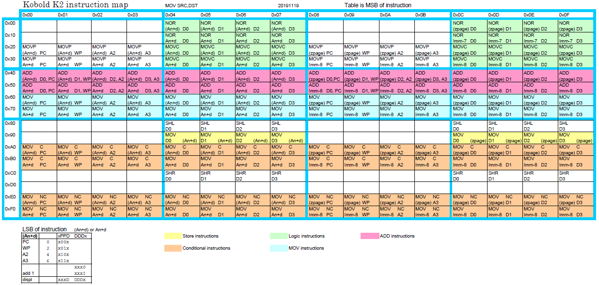
Instruction Map
11/19/2019 at 16:17 • 0 commentsAfter making many changes, it seems that the instruction set is now finally stable. The instruction set is now very orthogonal. An instruction map was made, that clearly shows the meaning of the upper 8 bits of the instruction (Click on it for a readable version. Excel file is in the file section).
![]()
There are four addressing modes:
- (An+d) Register indirect with 4-bit displacement, includes 16 bit immediates. The result can optionally be incremented by 1.
- (zpage) One of 128 locations in the zero page (lowest bits in instruction)
- An+d The value of an address register, incremented with 5 bit constant. Also used for short jumps.
- Imm-8 an 8-bit constant (lowest bits in instruction)
Almost all instructions write the result to one of the four 16-bit data registers, or one of the four address registers (this includes the PC).
The most used instructions have a color in the map, from top to bottom:
- Green, logical NOR and MOV-Complement.
- Pink, 16-bit ADD
- Blue, MOV instructions (including jumps)
- Yellow, MOV to memory (store)
- Orange, conditional MOV instructions (including conditional jumps)
There are several empty positions in the map, so there is room for an extended version that has more instructions.
-
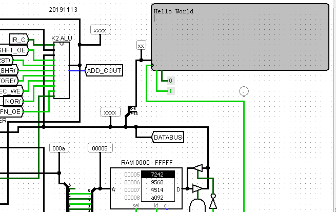
Hello simulator !
11/15/2019 at 15:53 • 0 commentsToday a minor milestone was reached.
The javascript assembler is working (for most instructions). I didn't work yet on the Javascript simulator .
But I also have a Logisim simulator. The assembler output for 'Hello World' was loaded in the Logisim simulator, and it worked ! It's the first real running program written in Kobold Assembly !
![]()
The program is this:
            0 ; Kobold K2 assembler test
            1
            2 screen: equ 0xf000
            3 newline: equ 0x0d
            4
00000 7C00  5  mov 0,d0
00002 7A20  6  mov text,a2
00004 631E  7  mov screen,a3
00006 7008+ 8 loop:
00008 6540  9  mov (a2),d1
0000A 7242  10  add 2,a2
0000C 9560  11  mov d1,(a3)
0000E 4514  12  add 0xffff,d1 ;test for zero
00010 A092 b13  brc loop ; branch if non zero
00012 700C+ 14 hlt: jmp hlt
00014 6084
            15
00016 AAAA  16  data section
00018 0014-
0001A 0008-
0001C FFFF-
0001E F000-
            17
            18 text:
00020 0048  19  dw 'H'
00022 0065  20  dw 'e'
00024 006C  21  dw 'l'
00026 006C  22  dw 'l'
00028 006F  23  dw 'o'
0002A 0020  24  dw ' '
0002C 0057  25  dw 'W'
0002E 006F  26  dw 'o'
00030 0072  27  dw 'r'
00032 006C  28  dw 'l'
00034 0064  29  dw 'd'
00036 000D  30  dw newline
00038 0000  31  dw 0
Some remarks:
- In the instructions, source comes before destination: MOV SRC,DST
- The first instruction (mov 0,d0) is non-functional, because execution after reset skips the first instruction
- There is no HLT instruction. A the end of the string, the program just keeps jumping to the same HLT label.
- Note the use of the ADD 0xffff instruction to test for zero. That's because there only is a carry flag, no zero flag.
- Immediates that do not fit in 8 bits are 16 bits and placed at the end of a 16 word chunk, and flagged with a '-' for the human reader. so you find the 0xffff for the 'test for zero' on address 0x0001C. The values 0014 and 0008 are for branches to loop and hlt, to be discussed later.
- The logisim textscreen responds to writing to every address of 0x8000 and higher. The textscreen has the address 0xf000 in this example.
- The Logisim simulator can not read bytes from memory, so the text has been placed in words. The actual CPU wil be able to read bytes.
- Line 13 is marked 'b' and lines 8 and 14 are marked '+', both will be explained later.
- Actually, the page registers of A2 and A3 should have been set to 0 with an instruction, but in the simulator they are already zero by default. However, the reset hardware does set the page of PC to zero.
The Logisim file and the file to be loaded in the Logisim RAM are in the file section.
The assembler can be tried here: Kobold K2 Assembler. Just press 'Assemble' to run the assembler. Feel free to try some code changes. The assembler can load/store files from/to your own PC.
-
New instruction set
11/03/2019 at 13:57 • 0 commentsHere is the new instruction set. It is quite conventional (thats my personal view), but has a few quirks due to the fact that a lot of functionality was pushed into the instruction set, while keeping the decoding circuits very simple.
I will present the new set in three encoding tables, starting with a few simple ones.
(There is also a colored instruction map available)
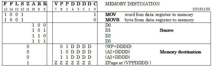
WRITE TO MEMORY
![]()
There are two ways to address memory:
- Pointer with displacement. WP, A2 and A3 can be used as pointer (PC should be used for reading only).
- Zero page. Zero page size is 128 words (256 bytes).
All four data registers can be written to memory, either as word or as byte. To write an address register to memory, first move it to a data register and then write it.
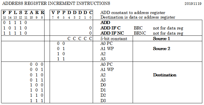
INCREMENT ADDRESS REGISTER
![]()
Address registers can be incremented with a value from 1 to 31. This can also be conditionally, mostly used in combination with A0 (PC). So the branches can skip 15 instructions at most. For greater distances, 16-bit immediate conditional jumps must be used. Note that the destination of the addition can also be a data register.
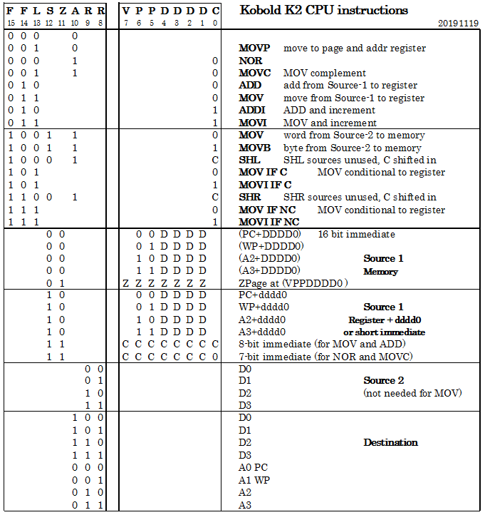
ALL INSTRUCTIONS
![]()
This may look a bit complex. But you just pick an instruction, one or two sources and a destination.
Note that there are several ways to specify the source operand:
- Address register indirect with displacement, (includes 16-bit immediate when addr register is PC)
- Zero page location
- Address register plus small (5 bit) constant
- short immediate (7 or 8 bit)
Oddities:
- The MOV to register instructions can be conditionally executed.
- A jump or branch is just a move or conditional move to the PC (register A0)
- There are MOV-with-increment instructions. One of its uses is incrementing a value in memory with just two instructions
- MOVI (value),D2 ; get value in D2 and increment it
- MOV D2,(value) ; store value back
- ADD-with-increment (ADDI) is just adding with the Carry-input of the ALU set. Useful for subtraction.
- For SUB, use MOVC (Move and complement) followed by ADDI (Add and increment)
- For AND and OR, use NOR in combination with COM (Complement) or MOVC (Move and complement). COM is the same as NOR with #0.
- For MOV (and ADD) with 8-bit immediate, the lowest immediate bit is formed by choosing between the MOV and MOVI instruction. The assembler will handle this. Since this lowest immediate bit is connected to the carry-input of the adder, it is not available for the logical functions NOR and MOVC.
- SHR instruction acts on the result of the previous instruction.
- The SHL instruction writes to memory as a side-effect. The assembler will use the highest zero-page word (at 0x00FE) as location to write to.
Remarks for address register destination:
- ADD instructions have 3 operands, the source-2 operand is always a data register, and the number of the source-2 data register must be the same as the number of the destination address register. So ADD A1, D2,A2 is possible but ADD A1, D2,A3 is not possible.
[ edit 20191115: I pushed some more functionality in the ISA, schematic in file section has been updated ]
[ edit 20191119: new schematic uploaded to file section ]
-
More conventional instruction sequencing
11/01/2019 at 22:02 • 0 commentsThis week I was working on the assembler again. As said in the previous log, the assembler is quite complex because it also has to place the instructions in the correct sequence.
Although the instruction sequencing and the conditional branching can be explained, the inner working of the assembler will be obscure due to its complexity.
And if we ever come to the point where programs can be built on the machine itself, we also need an assembler that runs on the machine itself, so that must probably also be written in assembler (while the current assembler is written in Javascript). I shivered at the thought of having to code this again.
So I decided. Design change.
Thats the nice thing about a hobby project. You can keep changing. Your project can even keep changing without ever coming to an end....
The instructions wil be in sequence. There will be a hardware 4-bit program counter, that will address the instructions together with the other bits in the HC670 register, much like the Kobold-one.
At the end of a 16-instruction block, a jump instruction must be placed to go to the next block. This will be done automatically by the assembler. Conditional branches will now also be done in a conventional way.
The three NNN bits that hold the next slot number can now be used for something else. This will make the decoding of the special instruction variants easier, and give room to provide more options for some instructions.
[ edit: In fact, the instruction variants vanished, making the ISA much more orthogonal. There is now also room for 8-bit immediates within the 16 bit instruction, and zero page size expanded to 128 words, see next log. ]
-
Changing the memory access model
10/16/2019 at 17:52 • 0 commentsIn the past weeks, I did first draw the design in the Logisim simulator. The first few instructions were succesfully simulated. Then I started working on a Javascript assembler-simulator combination.
While I've been making assemblers in the past, this one proved quite difficult. You'll remember from one of the previous logs, that the instructions can be arranged within 8-instruction blocks in almost arbitrary ways. But the actual sequence becomes important for flow control and optimization of (conditional) jumps. Above that, each 8-instruction block must end with a jump to the following block, and sometimes a slot in a block stays unused because there is a multi-word instruction or instruction sequence that can not be distributed over two blocks.
The goal was, that the assembly programmer doesn't have to concern himself with the above subtleties, and that the assembler program does all this. Now in a 'normal' assembler, the instructions have almost no interaction with each other. That's totally different now.
But now that the struggle to do automatic instruction sequencing by the assembler has almost been completed, an inconvenience in the design came to the surface of my mind. That is the memory access system.
The proposed system has two models, the linear and the object model. This forms a kind of two-dimensional memory system with the A0-A15 address on one axis, and the page-or-displacement value on the other axis. If a language like C would do memory allocation, using the Kobold system, that would mean that memory would be allocated in two dimensions. This would give a lot of complications.
So I decided to change to a more common model, while keeping most of the advantages of the 'old' system. The schematic of the old model is still available as version 20191011.
NEW MEMORY MODEL
In the new memory model, the object system has become a part of the linear model. It is almost the same as in the Kobold-one.
The address of an operand is formed by:
- A0: from address register. Is high for byte-access to the MSB of a word.
- A1 - A4: from address register. The four displacement bits are added to this.
- A5-A15: from the address register
- A16-A19: 4 bits from the page register that belongs to the address register
An instruction can have a 4-bit displacement that is added to bit A1 - A4 of the above address. The result determines the position of a memory operand.
The address of the next instruction is constructed as follows:
- A0 is always zero, because an instruction is a word.
- A1, A2, A3 come from the NNN bits in the current instruction
- A4 - A15 come from address register A0 (PC, program counter)
- A16 - A19 come from the page register of the program counter
You see that the lowest four bits of the program counter are not used to address the next instruction. That opens the possibility to store a copy of the program page in those four bits. This gives us the same more-than 64K jump capability as in the old model, for instance for return address storage:
- The PC is moved to a dataregister, and the subroutine stores it in the stack frame
- At return, the stored address is written to the program counter, and to the page register of the program counter, at the same time! As before, the return address is always in the same instruction slot.
- So now the page register has correct contents, because that was previously stored in A0 - A3. And A4 - A15 will be used to fetch the instruction, together with the page (A16 - A19).
And, also, a jump or call is still able to reach all memory positions without a near-or-far mechanism.
The schematic is now updated. The log Addressing modes was also updated.
-
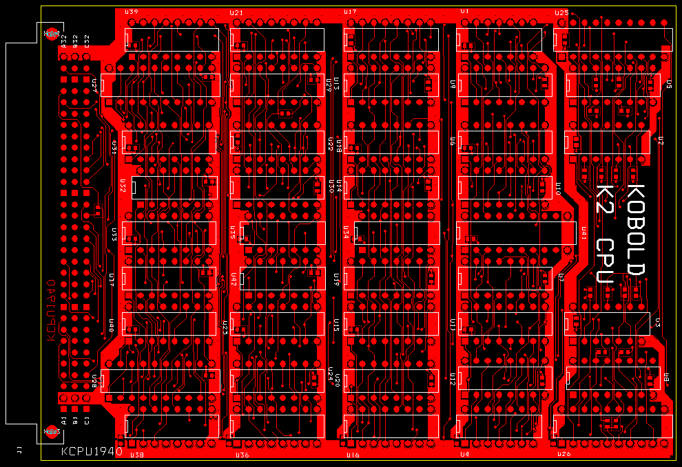
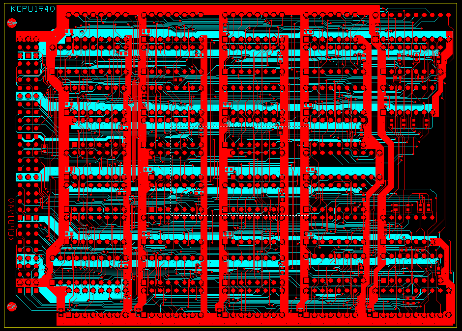
PCB impression of the CPU
10/04/2019 at 18:54 • 0 commentsA colorful log this time.
The CPU is completely routed now. I used a mix of automatic and manual routing.
I chose a DIN41612 connector for the CPU (3 rows of 32 contacts). The middle row of contacts is not used.
The PCB size is 4.0 x 5.575 Inch ( 10.24 x 14.15 cm ). Clicking on the pictures gives a slightly larger image.
You will see component placement, top layer, bottom layer and their combination here. Clicking on the pictures gives a slightly larger image.
![]()
![]()
![]()
-
CPU schematic explained
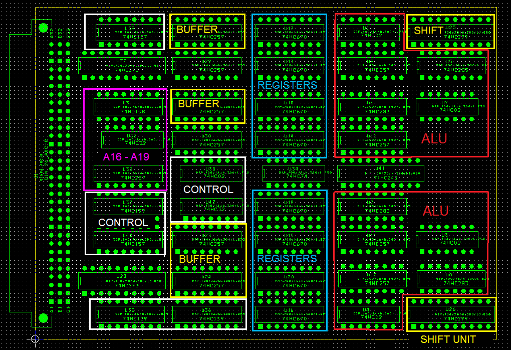
10/02/2019 at 19:31 • 1 commentThis will be a quite long log.... luckily, it will naturally stop when all 42 IC's have been explained...
This will be a detailed description of the schematic. For a good understanding, first read the first log and the logs that follow it.
The schematic was split into nine sections, that will be discussed:
- Instruction register
- ALU
- Data and Address registers
- Shift unit
- Buffer unit
- Page registers
- Control
- Bytewise memory access
- Specials
I want to start with something simple, the ALU, but let's first do the instruction register because allmost every subcircuit is connected to instruction bits.
[edit: this describes an older version of the schematics, it needs an update]
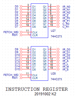
INSTRUCTION REGISTER
![]()
The instructions are 16 bits wide. The register gets written during the FETCH cycle. Its outputs are (from top to bottom):
- N0, N1, N2 hold the slot number of the next instruction
- Z, that is active for ZPAGE (and vector) addressing
- P0, P1 select which of the four registers A0 - A3 puts its contents on the address bus
- R0, R1 select D0-D3 as source register, and D0-D3 or A0-A3 as destination register
- D0-D3 select the displacement (0-15) that is put on A16-A19 of the address bus
- A, L, M, S are the instruction opcodes, mainly connected to:
- A is 0 for an address register destination, 1 for a data register destination. For writing to memory, it selects between writing a word and writing a byte.
- L is 1 for forcing the first ALU input (signals OP0-OP15) to zero (by disabling the data register output and using pulldown resistors). This will change ADD to MOV and NOR to MOVC (MOV-complement)
- M selects (when S=0) between ADD and NOR in the ALU, and (when S=1) between register-to-register operation and a move to memory
- S is 0 for an ALU operation with memory operand, and S is 1 for register-to-register operation or a move to memory.
Note that during reset, the instruction is forced to 0x0000. The function of the instruction bits and their combinations can also be found in the Instruction encoding log.
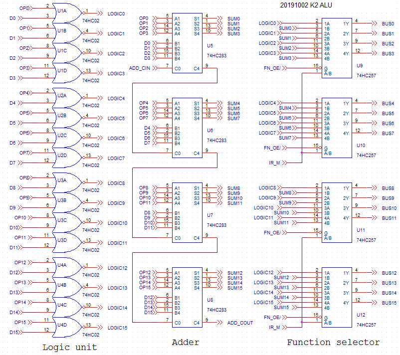
ALU
![]()
The ALU is quite simple. There are two input busses, D0-D15 that normally come from memory, and OP0-OP15 that come from one of the data registers D0-D3. Outputs are BUS0-BUS15.
At the left side, you see 16 gates that perform the NOR function on the two inputs. In the middle, four HC283 adders will add both inputs. At the right side, a bunch of multiplexers will choose either the NOR or the ADD as a result on the result signals, called BUS0-BUS15. The IR_M signal comes from the instruction register, and provides the selection signal for the multiplexers.
Note that the multiplexers that deliver the BUS0-BUS15 signals can be put in high-impedance state with the FN_OE/ signal, and the adder has a carry-in and carry-out, both to be discussed later.
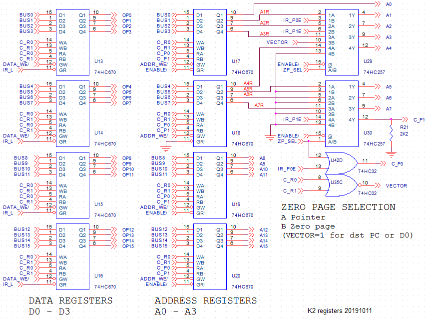
DATA AND ADDRESS REGISTERS
![]()
The data and address registers are built with the 74HC670 (that chip is explained HERE). There are 4 data registers and 4 address registers, these are all 16 bit wide. (These are actually latches instead of registers, to be discussed later).
The input to the registers is shown at their left side. The data bits come from the ALU (they are connected to BUS0-BUS15), and the R0, R1 bits determine which of the four registers in the IC gets written (when DATA_WE/ or ADDR_WE/ is low).
The output of the data registers is connected to the OP0-OP15 bus. One of the four registers is selected with the same R0, R1 signals. Note that the IR_L bit, coming from the instruction register, can disable the register output. The outputs will then be pulled low by pulldown registers (on another part of the schematic). Since the OP0-OP15 bus is one of the inputs to the ALU, this will change an ADD instruction to a MOV and a NOR instruction to MOVC (MOV-complement).
The output of the address registers is selected by P0 and P1 coming from the control section, but when ZPage addressing is selected, this will always be A1 (the workspace pointer WP), so the WP provides the upper address bits for the zero page.
At the right side of the picture you find two multiplexers that connect most of the lower address bits to an alternative source when Zpage addressing is used. Bits A1 and A2 are in that case connected to P0 and P1. Together with the four displacement bits this gives 64 possible "zero page" locations. Address bit A3 will be 1 when the destination is register A0 (PC) or D0, providing another 64 locations as quick jump vectors.
Note that the address outputs can be tri-stated with the ENABLE/ signal. That is connected to the I/O connections of the CPU, and can be activated by another device when it wants to access memory.
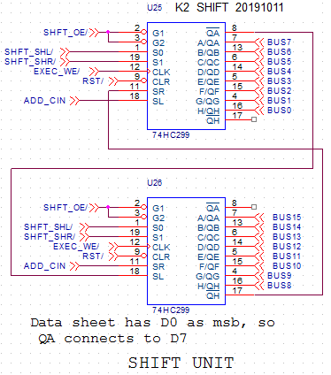
SHIFT UNIT
![]()
The previous mentioned 74HC670 register chips are cute, but have a disadvantage. They are latches, not registers. So if one of the registers is connected to the ALU, and the ALU result is written back to the same register, this new value immediately goes to the output, creating a feedback loop that makes all logic levels in this loop totally unpredictable.
Therefore, during the execute phase the ALU result is stored in the shift unit (with the EXEC_WE/ signal). During the following fetch phase, the data is copied from the shift unit into the destination register. The correct destination register is still selected because the instruction register contents will be stable until the END of the fetch phase.
The shift unit is built with 74HC299 register chips. They have each input at the same pin as an output. so by connecting its 8 pins to the BUS signals, we can load data from the bus and also put data on the bus. And instead of loading from the bus, it can also shift its data (in both directions).
So during exec the BUS is driven by the ALU (FN_OE/ signal connected to the muliplexers of the ALU), and during fetch the BUS is driven by the shift unit (SHFT_OE/ control signal connected to HC299).
Two 74HC574 could have been used here to break the feedback loop, but using the HC299 gives us a shift function for free. It is only a bit awkward to use it, because when activated (with SHFT_SHR/ or SHFT_SHL/ signal) the current ALU output is unused, and the ALU output of the previous instruction will be shifted at the rising clock edge and written to the destination in the fetch phase that follows. Since shift is not frequently used, this seems acceptable. In a shift instruction, another specific bit in the instruction tells if a 1 or 0 will be shifted in (ADD_CIN signal).
Finally, the shifter is connected to the reset (RST/). The reset signal also forces the instruction register to 0x0000 (as mentioned before). This instruction selects the program counter as destination. It does not matter which value the ALU calculates, because the shifter is now zero, and zero will be written to the PC. So after the reset, the CPU will start executing from address zero.
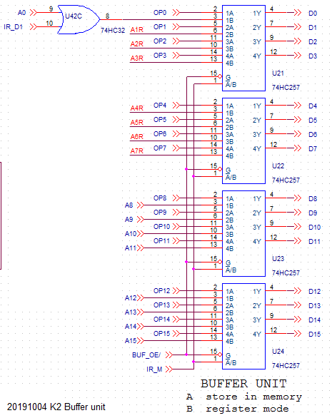
BUFFER UNIT
![]()
The buffer unit has two functions:
- For storing a dataregister in memory, transfer data from the OP0-OP15 dataregister outputs to the datalines D0-D15 (that are connected to memory).
- For instructions that use an address register-operand instead of memory operand, connect the outputs of the address register A0_A15 to the D0-D15 datalines that connect to the ALU.
A set of multiplexers with tri-state output combines both functions. The output-enable (BUF_OE/) is active when instruction bit S is high (in that case, the memory output will be disabled). Instruction bit M is connected to the select input and selects between data register (OP0-OP15) and address register (A0 - A15). Note that for A1-A7 an address is used that is taken before the final Zpage-multiplexers. This is mainly to simplify the pcb routing.
You will also notice a gate in the A0 signal. For incrementing the PC, we can increment it with the ALU but that will only increment by 1 (when the carry-in is set), while the PC is a word address and must be incremented by 2. By forcing the A0 signal to 1 before incrementing, the result is that the PC is incremented by 2 (knowing that it always contains an even address). The same method can of course be used to increment other address registers by 2. The gate is controlled by displacement bit IR_D1, that is not used for the displacement in this instruction where the operand comes from an address register and not from memory.
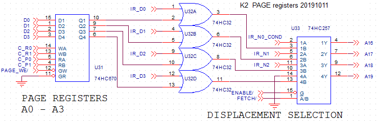
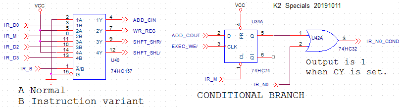
PAGE REGISTERS
![]()
Each address register has an associated page register. It is written directly from the databus when the control unit activates PAGE_WE/. Its output value is or'ed with the 4-bit displacement value that comes from the instruction register (described in accessing memory).
At the right side we see a multiplexer that will:
- During the exec phase, provide the mentioned page-or-displacement value on A16-A19
- During the fetch phase, put the N0, N1, N2 bits on A16-A18 (A19=1), to fetch the next instruction from the specified slot. The N0 signal might have been modified by the branch-condition logic (so it is called IR_N0_COND here).
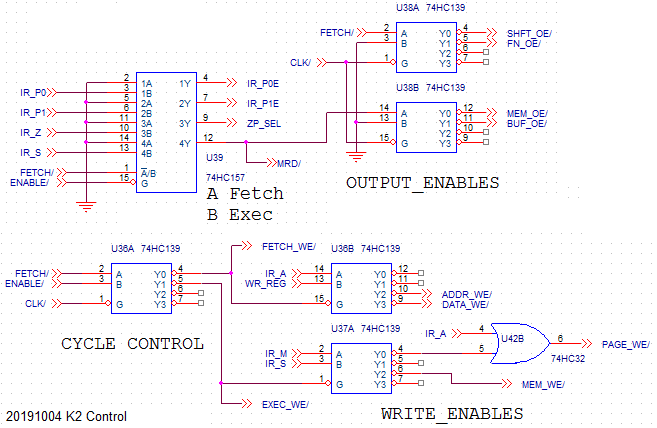
CONTROL
![]()
Here we come to the reason of existence of the Kobold K2. Many TTL CPU designs are microcoded and have several EPROMS with microcode (I've seen up to 7) and a lot of control wiring. Getting rid of the microcode was one of the goals of Kobold 2. You see here that the resulting control system is really simple. It's heart, that is shown here, uses only around 4 TTL chips.
We start with the 'Cycle control' at the left side. It is driven by 3 external signals:
- an active-low clock signal
- a FETCH/ signal that must toggle between 1 and 0 when the clock is inactive
- an ENABLE/ signal that must be active for the CPU to operate. This signal is de-activated by another device when it wants to access memory.
The control system will distribute the clock pulse:
- to FETCH_WE/ for a fetch cycle. Used for a write to the instruction register.
- to ADDR_WE/ when data from shift unit must be written to an address register
- to DATA_WE/ when data from shift unit must be written to a data register
- but a write to data or address register is only done when WR_REG is active (comes from instruction-variant special section)
- to EXEC_WE/ for an execute cycle. Used for a write to the shift unit.
- to MEM_WE/ for S=1 and M=0, for writing to memory
- to PAGE_WE/ for S=0 and M=0 and A=0, to write to a page register
In the upper left part there is a multiplexer that modifies four instruction bits during fetch phase. In the fetch phase, we must be sure that the PC (register A0) is connected to the address bus. This is done by this multiplexer. It forces the address-register select signals P0 and P1 (here called: IR_P0E and IR_P1E) and the Zero-page selection to zero. It also enforces a read from memory (MRD/).
In exec phase, when the S bit is 0 it will enable the memory read (MEM_OE/) and when S is 1 it will enable the buffer ouput (BUF_OE/).
Finally the decoder in the upper right corner generates enable signals to connect either the ALU output (FN_OE/ active) or the shift unit (SHFT_OE/ active) to the BUS0-BUS15 lines.
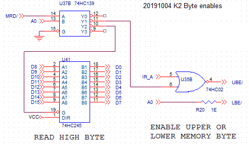
BYTEWISE MEMORY ACCESS
![]()
For reading a word, MRD/ will be low, and address bit A0 will also be low. So the Y0 output of decoder U37B will be active (low) and the other outputs inactive (high). So the "read high byte" buffer is not activated, the NOR gate U35B will output low, so both UBE/ and LBE/ (upper and lower byte enable) will be active (low). Both bytes in the word will be read.
For reading a byte from memory, the A0 address line can be low or high (for reading LSB or MSB). When reading LSB, the instruction acts exactly the same as for reading a word. So a full word will be read. The programmer might, in the destination register, set the upper bits to zero (in a following instruction) if these bits bother him/her. For reading the MSB from memory, the Y2 output of the decoder is activated, so the "read high byte" buffer will put the D8-D15 bits of the databus to the D0-D7 bits. At the same time, since A0 is now high and connected to LBE/, the lower byte of the memory will be disabled, and that is needed because this lower byte now comes from the "read high byte" buffer.
For writing a word to memory, instruction bit IR_A is 1, and MRD/ wil be inactive (high). No decoder outputs will be actve. Both UBE/ and LBE/ (upper and lower byte enable) will be active (low). Both bytes in the word will be written.
For writing a byte to memory, instruction bit IR_A is 0. The programmer should make sure that the byte is in the LSB as well as in the MSB of the word that is written (because he normally will not know if it is written to an even or odd address). Now all there is to do, activate either LBE/ or UBE/ depending on the value of address bit A0. When A0 is low, output Y1 of the decoder is activated (low), and because IR_A is also low, the NOR gate will put high (inactive) on the UBE/ signal. So the upper byte is disabled and only the lower byte gets written. When A0 is high LBE/ is also high, the lower byte of the memory will be disabled and only the upper byte gets written.
The assumption is, that bytewise access will be used a lot less than word access. Therefore it was accepted that the programmer has a bit more work to do here, instead of using more TTL to implement the bytewise access fully.
SPECIALS
![]()
And finally, some odd ends, that nevertheless are needed for operation.
- Instruction variants
As mentioned before, there is a register-to-register instruction group that does not reference memory. The displacement bits in the instruction are not used in that case. The multiplexer is used to provide a function for these bits when there is no memory access. The four bits are used as follows:
- D0, when 1, sets the carry-in of the ALU. Needed for subtract and multi-precision addition.
- D2, when 0, lets the shift unit shift its previous contents to the right, instead of loading it from the ALU.
- D3, when 0, lets the shift unit shift its previous contents to the left, instead of loading it from the ALU.
Displacement bit D1, when 1, sets bit A0 of an address register on its way to the buffer unit. Together with the carry-in, this enables incrementing an address register by 2. This was mentioned in the buffer-unit explanation, but is also mentioned here because it is considered an instruction variant (although this multiplexer is not used for this function).
The multiplexer also generates the WR_REG signal, that is 1 when a register must be written, but 0 when it must not be written because something is stored in memory. The WR_REG signal is used by the control section.
For instructions that read memory, the instruction-variant outputs are set to their default value by the multiplexer for S=0. For the store-to-memory functions, the instruction variant is selected, but that does no harm because the variants only affect ALU output, and the ALU output will not be used in a store-to-memory instruction.
- Conditional branch.
In the execute phase, the 74HC74 flipflop will be set to the state of the carry-out of the adder in the ALU. In the fetch state that follows, bit N0 (the lowest bit of the instruction slot selection) is forced to 1 when the carry was one. The flipflop will be kept in reset when instruction bit M is zero, no branches in that case. And when bit L=1 (data register output is 0) there will also never be a carry because the adder has 0 (from the data registers) on one of its inputs. Isn't it amazing that you can implement conditionals with just a flipflop and a gate ?
It was long... are you still with me ? I don't hear anything. You must be asleep by now...
[ EDIT 2019115 Several changes were made to the CPU. The above description will have to be changed. ]
-
Schematic of the CPU
09/18/2019 at 19:34 • 0 commentsWhat you have all been waiting for....
The first version of the schematic for the CPU was just uploaded to the file section !
A few things were added:
- Provision for reading and writing bytes from/to memory. Address bit A0 will select low or high byte (as with most processors). Writing bytes will need software assistance. Single-cycle reading and writing of 16-bit words is of course still possible.
- The 64-word Zero page has got companion of another 64-word zero page. The second zero page is called the vector page, and is automatically selected whenever zero-page contents is written to the PC or D0 register. This is ment to be used for frequently accessed subroutines. A call can get its address from the zero page, saving space for an immediate value in the program code. The D0 register can also be used to store a value in the vector page.
The connectors of the CPU will probably change.
Explanation of schematic will be done in a next log.
Number of chips grew slightly above 40, it is now 43.
[ edit: schematic updated today, 20191023 ]
Kobold K2 - RISC TTL Computer
A 16 bit RISC computer with video display, from just a few TTL and memory chips. Online C compiler and simulator available.