Close
0%
0%

Super Micro Relay Computer

Going back almost 200 years, to what could have been the very early beginning of electronic computing!

Similar projects worth following
The computers built with relays had an effimerous life, but boldly marked the transition from the Babbage's mechanical world to the modern active electronic era.

This project proposes a *minimal* but powerful design (with two registries, full set of ALU ops, direct and indirect conditional jumps) of what could have been a micro computer built in the middle of the 1800, also affordable and easily buildable today!

There are many reasons for being interested in these type of realizations, as:
- Relays are among the simplest electronic components and this make easier to understand the very basic and very internal computer processing mechanisms
- The design is based on modern patterns (registries, ALU, RAM, control logic with flags and conditional jumps, etc)
- Is possible to hack on them with extremely basic and limited equipment
- They are fun to build and to run, with more poetry in seeing and hearing things moving than in the silence and immobilty of their silicon compeer

Building a relay based computer is surely the ultimate retrocomputing experience, and  my wish is to try to engineer what could have been the very first electronic computer.

With this build I will also try to teach to my daughter some concepts regarding computers that are difficult to see from an high level perspective, and hope also others will find it useful fun and educational!

The goal of this particular implementation is trying to minimize the number of relays removing all possible redundancies still maintaining all the characteristics of a general purpose modern computer. New optimal designs have been already proposed for ALUs (https://hackaday.io/project/167879-optimized-alus-for-relay-based-computers), and here there is a similar continuation for the rest of the computer.

Less relays means a cheaper project, but also easier and faster to build and less space consuming (never too much)!

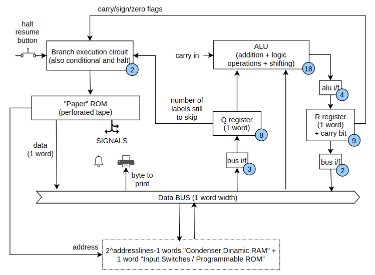
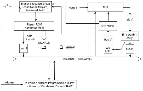
Below the "high level" architecture:

Please note that the 2 registers are called Q and R instead of the usual A and B just to avoid confusion with the ones described in the ALUs that are usually both input ones, while here R is the result register (that contains also the carry flag).

One of the key design differences among many of the current proposals is the utilization of punched tape for the program input. The main reason to opt for this choice is the obvious fitting with the period, but there are many others:

- Possibility to simply easily add more control signals simply adding more "hole columns" if needed
- No need for an external clock, since timing is embedded in the punched signals themselves; and this means less relays
- Easy sub shifting of the individual signal timing, and this means no need of complex clock circuits and more relays
- Possibility to easily regulate overall speed, simply changing the speed of rotation
- Writing directly signals there is no need for decoding logic; this means fewer relays but also faster execution
- Primitive and inexpensive technology available even before the period
- No limit of program length
- No need of PC counter and separate bus (or access logic); this means fewer relays, even though there is the need for circuitry to manage the jump instructions
- Tape program input is faster than manual input (e.g. with switches values stored in RAM) and more elegant and appropriate than EPROM solutions

Surely the fact that there are not already ready modules and a custom build is required is a cons, but the willingness to avoid using more modern technologies is a key factor. Anyway I hope to be able to find an easily buildable solution, and in internet there are already very simple ones to take inspiration from.

For the branch execution management circuit I will fully reuse the ALU (that has an arrangement thought also for this purpose), saving dedicated relays. The control will happen with some parallel dedicated signal support (saving firmware logic and more relays).

Again trying not to use silicon based solutions, regarding RAM I'm working on an original design based on capacitors. The direct memory access (with addresses coming directly from the program) reduce even more the relay count without really affecting programming potential.

Output will be visible on registry relays lamps. Punching cards would be very nice, but this might be a very last addition since the device will not be so simple to be built at home. Instead there will be probably the interface with a parallel printing device. An audible buzzer is completing the capabilities.

On the input side there are a set of switches addressed as the memory and a button to restart execution after halt instruction. More inputs can be read halting the execution between them.

The PC will support an «high level» instructions compiler, but can be also microprogrammed in order to have full control and optimization possibilities.

The supported instructions are by categories:

"data moving"...

Read more »

  • 46 × 4pdt relays for the main unit (not all required to be 4pdt in case)
  • 20 × meters of 0.5mm2 copper wire

  • Memory module

    Stefano12/08/2020 at 21:44 11 comments

    As mentioned the memory is one of the two remaining parts of the computer to be built (the other one being the mostly mechanical punched tape reader).

    For this I've tried to see if a ready design was available, but until now I didn't find anything suitable. Many relays computer implementations I've seen are attached to modern static RAM with some adaptor. The others are using diodes, as the TIM8 one, but I'm trying to avoid them in the construction since they were not available in the middle of 1800.

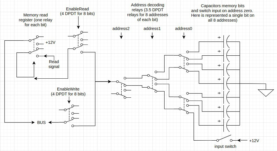
    The solution I'm thinking to implement is using just relays and capacitors. Not sure if it is the simplest as I'm always trying to push for, and I'm posting it here also to see if someone can improve it or suggest a new design.

    To write first erase content with EnableRead without Read signal, then switch off EnableRead and switch on EnableWrite and put on the bus what to write.

    To read switch on the Read signal than EnableRead will load the Memory read register with the value that is being put on the bus. Release the Read signal when the value is not anymore needed on the bus.

    Notes:

    1. The data is stored on capacitors, the relays form just the "memory controller" part

    2. Reading content "refresh" also the capacitors memory

    3. One of the addresses (zero in the example picture) is filled with switches instead of capacitors in order to save one control line and two relays that else should be dedicated to input read

    Relays count for 8 bytes (64 bits) memory:

    + 14 relays for address decoding (2+4+8)
    + 2 for EnableRead
    + 2 for EnableWrite
    + 8 for the Memory read register (can be dpdt)
    = 18 4pdt + 8 dpdt relays (plus 56 capacitors and 8 switches to complete the circuit!)


  • Main unit completed!

    Stefano12/08/2020 at 16:06 6 comments

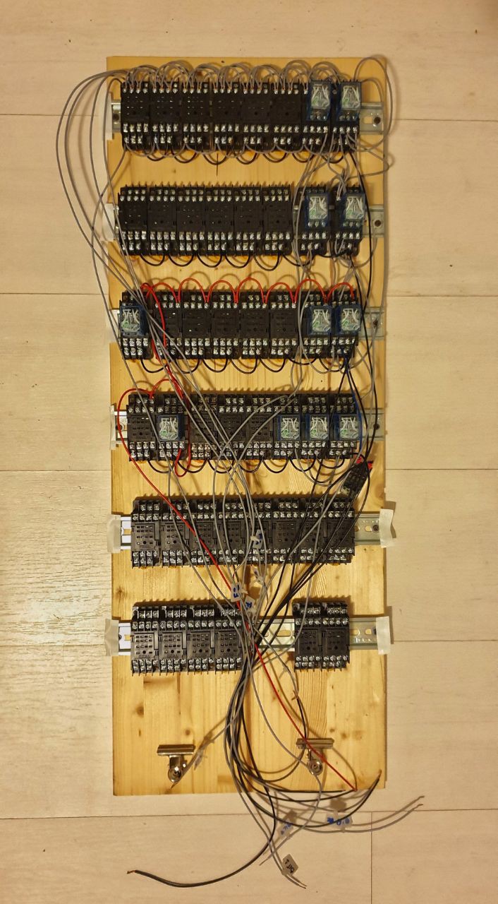
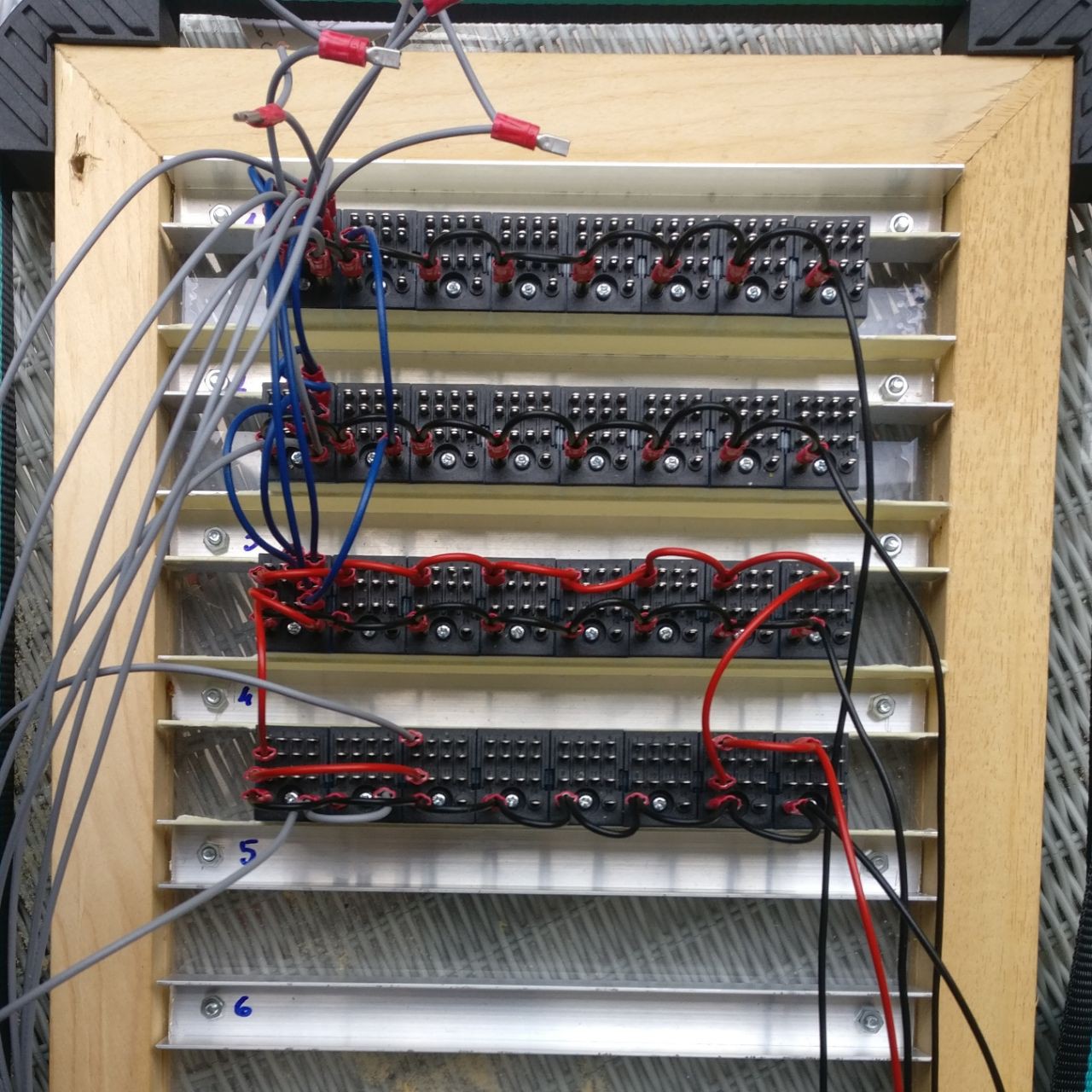
    With the usual slow but steady speed finally the main module wiring has been completed!

    And all functionalities tested worked as expected! There were just a few wiring errors but all of them cought during build time (one wire during the initial two bits test of the ALU, while all the others during immediate recheck of the step work done).

    Below the result:

    This is the main unit, missing "just" the random access memory module and the punched tape reader to be a complete system.

    This unit contains: 2 registries, a complete 8 bits ALU with carry bit in and out (able to perform all 16 logic operations, additions, and shifts in both directions), all the bus access interfaces required and the "halt" and "jump" management circuits to control the code flow.

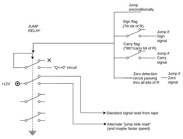
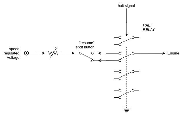
    Below some details regarding the implemented halt and branching management circuits (the one for ALU and Q register were detailed also here https://hackaday.io/project/167879-optimized-alus-for-relay-based-computers/log/186329-super-micro-relay-computer-cabling).

    BRANCH MANAGEMENT CIRCUIT

    The branch execution circuit is activated when one of the signal of jump "go through" the correspondent condition and activates the jump relay.

    Before the jump, Q should be set with the negative value of the numbers of labels to skip, and the circuit stops when Q is zero.

    During the jump execution the current is removed from "normal" tape signals and given to a section of tape dedicated to jump instruction where at each label there is:
    1. load R with Q+1 
    2. load Q from R

    When Q will become 0 the signal will automatically go back to the standard instructions side of the tape and instructions signals might also be written "longer" in order to be able to execute at faster tape rotor speed.

    Notes
    1. jump side signals and standard signals cannot be put on the same "line" since even if not active they might interfere in terms of connections.

    2. since the number of labels to skip is parametric call/return can be easily implemented (one memory location can be used for the return address) and also indirect jumps are supported by design
    3. backward jumps can be transformed into forward jumps if the paper tape is connected in a loop (buth the only forward mechanics should be much easier)
    4. to implement a real backward jump another relay should be required to invert the engine poles and to select a second side track that will do Q-1 instead of Q+1 (and with instructions in reverse order since the tape will move backward); this additional switch can be controlled by the higher bit of Q so effectively allowing a -127 to +127 range (instead of the current 1 to 255 labels)

    HALT CIRCUIT

    The halt circuitry is optional but very useful since apart at the end of the program can be used for example to input multiple values (or parts of a single larger input) with a cycle:
    1. halt (to allow input switches reconfiguration)
    2. move switches value to proper memory location
    3. go to 1 for the number of times required

    The configuration avoids that a single keypress skips more than a single halt since the press will advance tape until the halt signal on the tape will stop and to continue the button have to be released.

  • Slow but steady progresses

    Stefano10/20/2020 at 20:58 0 comments

    Long time has passed since last post, but things were moving, even if slowly.

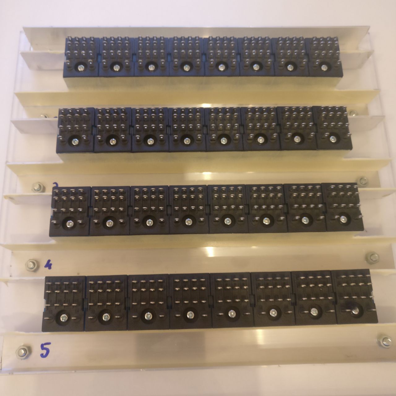
    In the meantime I decided to switch to relay socket bases, since faston connections were really too dense to be managed at the scale required.

    I also simplified even more the schema avoiding backward jumps: anyway I would not mechanically build them now, and I implemented them as forward jumps on a looped punched tape. This change would be noticeable in nested loops for very long programs but for now there are no plans for that (and in any case I can easily implement it later).

    The new schema is as follow (in the azure disks the numbers of relays):

    Totaling for a record 46 relays and nothing else (no resistors, no capacitors, no transistors and no diodes) apart a big mess of wires! :)

    The memory design is still open even if I already bought the required capacitors.

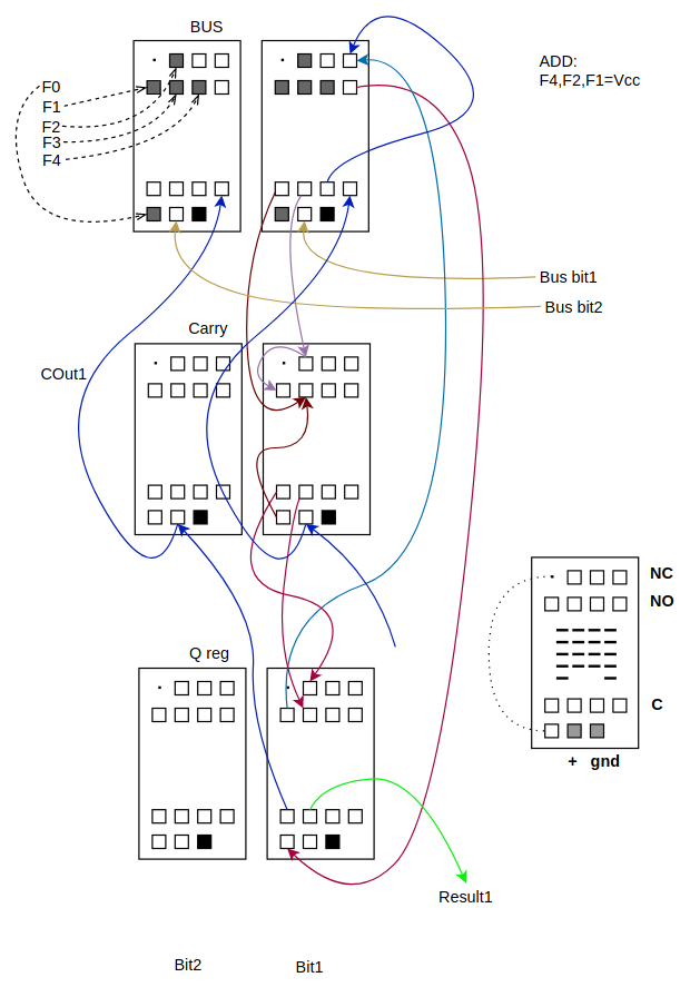
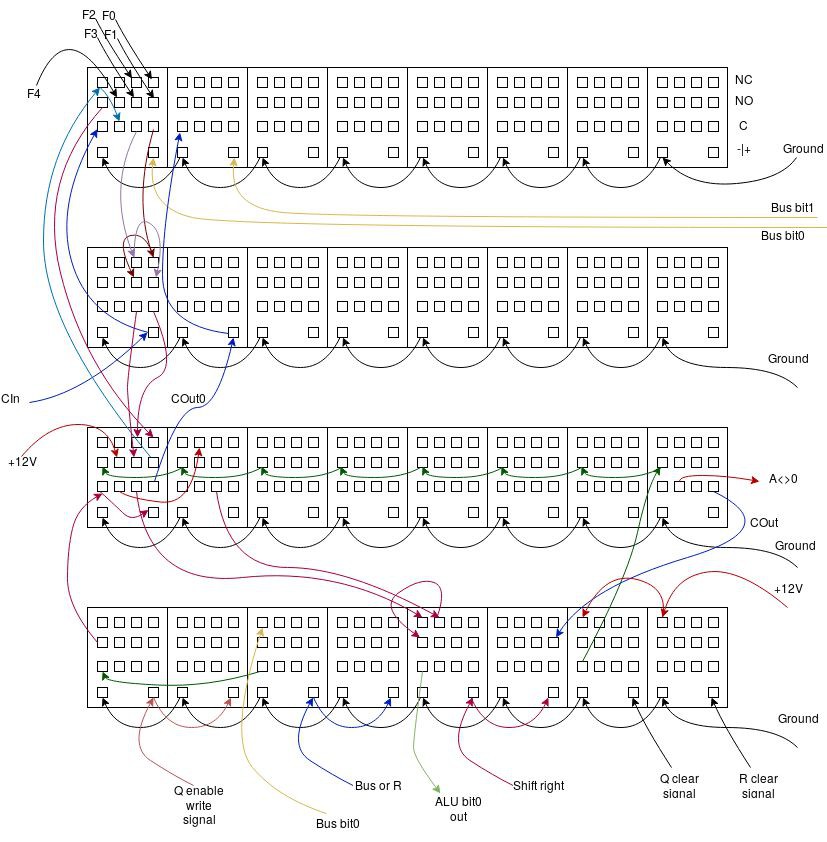
    With the bases the ALU needs a new connection cabling schematic (note that since relais are now seen from the top and not from the bottom as before, the bits endianness is increasing from right to left). Below a single bit slice with carry:

    This is the current work in progress:

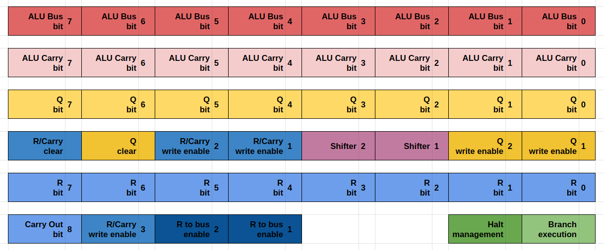
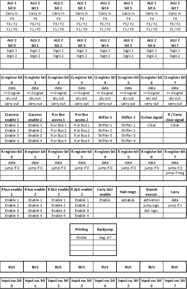
    And the relay placement matrix:

  • Click clack

    Stefano11/07/2019 at 08:42 0 comments

    The good news is: the first bit of the Q register and the ALU have been wired and they're working! Also proving that the more efficient ALU designs are a reality!

    I tested for convenience the full adder and for the logic part the NAND operation, but all other logic ones are straightforward to see operating.


    Below for example 1 of the Q register is added to 1 of the bus and a 1 carry in, resulting in a one on a "flying" bit of the R register and a carry out on second bit (note that relay view is upside down):


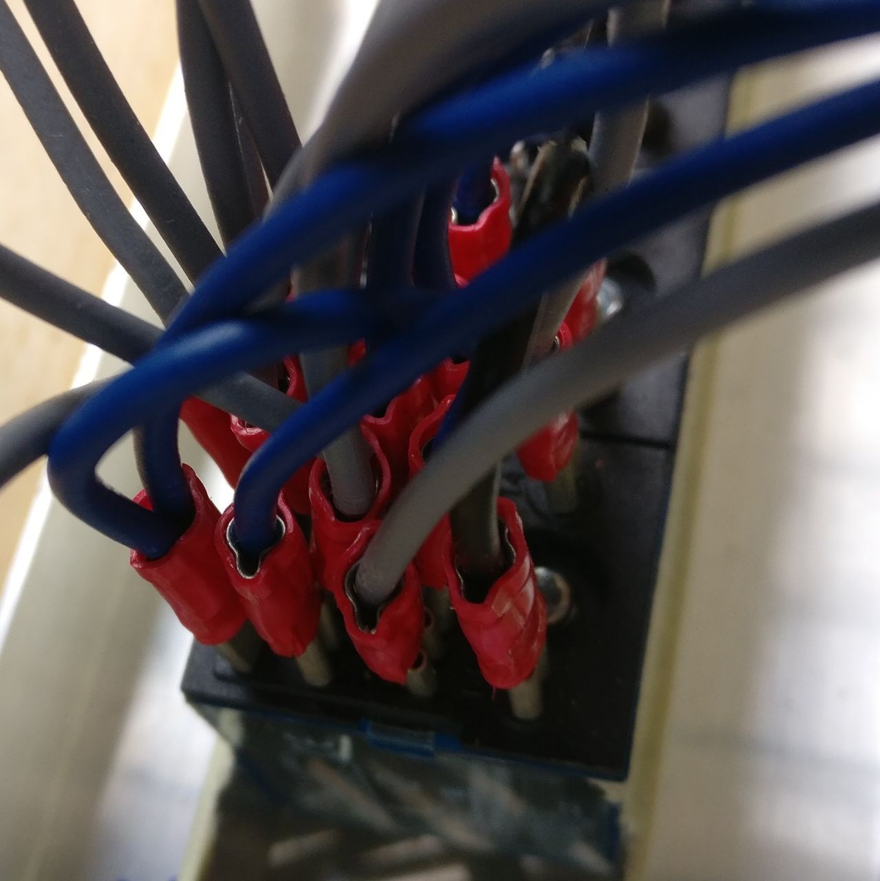
    The bad news is that mounting it with fastons as I did is extremely difficult with "dense" relay utilization...


    Faston are hard to slot in, and there is very little separation between them with even the risk of a short circuit on the bottom if two adjacent ones are slanted towards each other.

    Boefore continuing to mount the rest of the circuit I've to decide how to mount it. Options might be:
    1. Continue in this way, maybe finding a way to at least prevent short circuits (e.g. with a plastic foil between adjacent connected row of fastons)
    2. Solder the wires to the relays instead of using faston
    3. Buy relay bases and "easily" screw the wires (trashing all the effort spent on the frame, adding one month shipping time to the additional money to be spent)

  • Planning the layout

    Stefano10/28/2019 at 20:08 0 comments

    The frame start to get populated:


    50 might be a little number of relays but surely is already providing quite an intricate mess of wires and a lot of headaches if not properly planned (and even if properly planned): at least let's try to manage at best!

    Following a bit more detailed overall schema of the PC (more details of the various circuits will come in later posts):


    And below a tentative to put some order between units in the frame:

    As of last image a drawing guide for the wiring of the first bit of the ALU (the famous "no dollars" one of @roelh):

    (the full layout of the MY4NJ can be found in first project log)

  • Quality check

    Stefano10/28/2019 at 07:05 0 comments

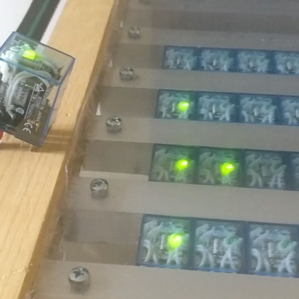
    First things first: let's start to see if the relays are properly working...

    For the purpose I built a little tester rig:
    Result? Bad. Out of the 62 relays I've found that 13 of them work unreliably and 3 not working properly at all. Partly good news is anyway that I've 46 remaining that seems working, let's see.
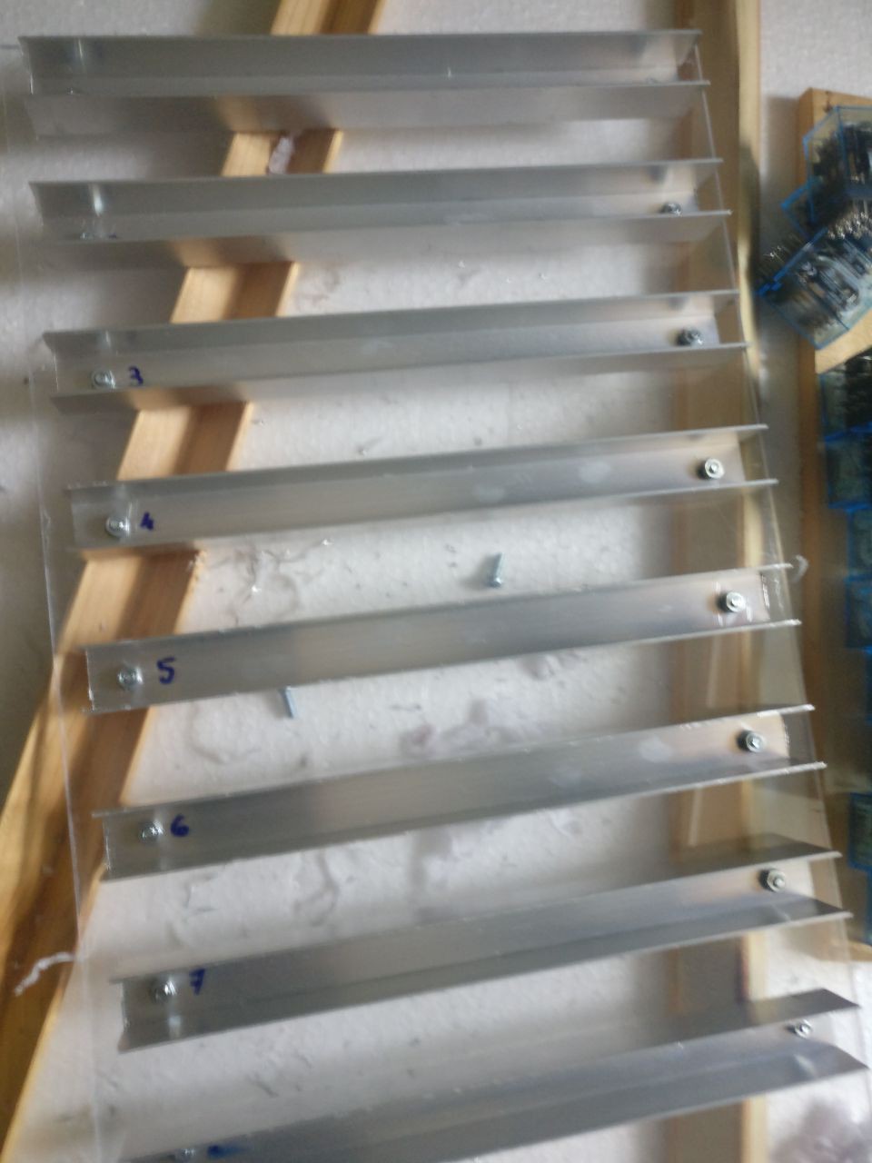
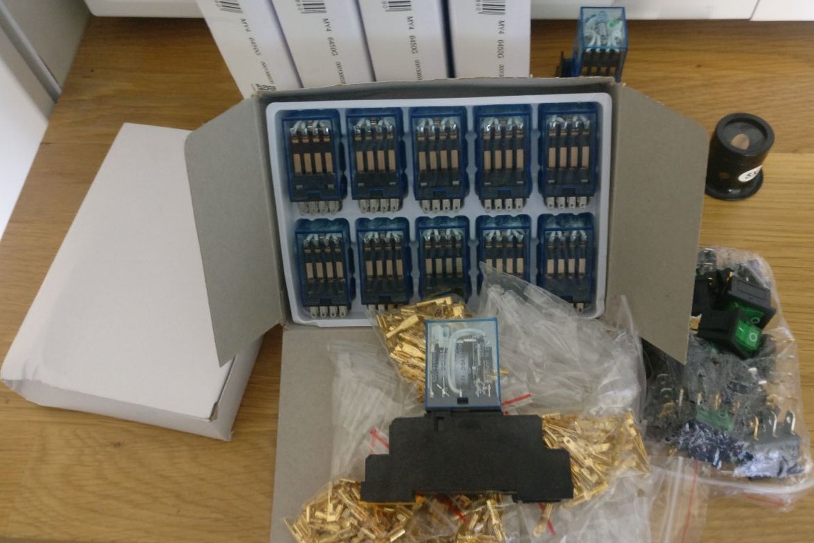
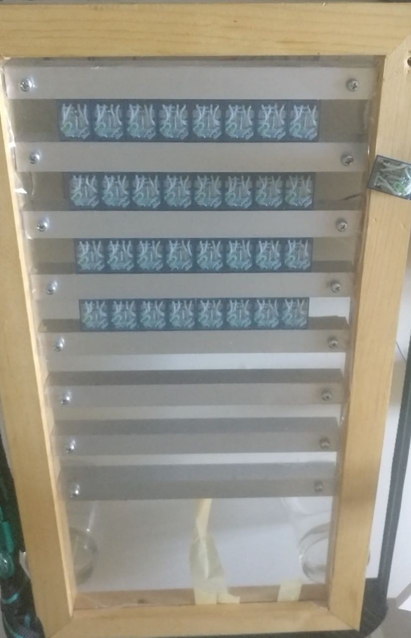
    In the meantime I built also a frame to keep the relays of the mounted computer. Here the last assembly step:


  • Let's start!

    Stefano10/20/2019 at 17:33 0 comments

    Relays finally arrived, and now it's time to start build the computer!


    I was liking transparent relays, where you can see the mechanism moving, and I found them at bargain price online. Buying SPDT, DPDT and 4PDT was practically same amount of money, so I selected all of them 4PDT, that will give also a uniform looking. Moreover 12V DC was the minimum available, and I’ve seen that this is a pretty common choice among other implementations. Looking at them afterwards they seems similar to the Harry Porter’s ones!

    I bought around 60 of them, hoping even to spare few with 8bit implementation... In reality I might spare even more realizing at least the first version with 4bit word lenght: easier to assemble, to debug, and anyway reaching all goals of the project, and "expanding" it later. I will decide building it. Anyway the design allows for the word to be any multiple of 4bit (e.g. 8, 16, 32 and even 64 bits) since there is no delay accumulation increasing the word size.

    The relays number in this moment do not account for the memory. For which I will probaly buy a different type (trough hole) for easyness of assembly with condenser (if the current design will work).


View all 7 project logs

Enjoy this project?

Share

Discussions

zpekic wrote 12/15/2020 at 17:08 point

Thanks for the clarification - you really have very "horizontal" microcode. I can see a problem of a very wide paper tape, I still remember the old printers fed with wide paper with perforation holes on two sides and how often they would tear even at small speeds :-( Two possibilities come to mind:

- reuse immediate data field for other purposes (in my microcode controller schema I use "else" field as immediate, the only caveat is those microinstructions cannot branch)

- group all that is needed for branching together, and all needed for execution together, and the multiplex them - this means each instruction is now two cycles, but that does not mean necessarily 2 as slow as perhaps branch condition propagation can be controlled better. 

I understand that for any of these a "control unit" is needed, which would be relay equivalent of 2n-to-n MUX controlled by the single bit. 

  Are you sure? yes | no

Stefano wrote 12/16/2020 at 00:42 point

Nice suggestions, I should try to think about them when implementing the reader (and one more I've added in the comment below that can very easily save 4 traces for the immediate data bits).

Regarding tearing I really hope not to be at least a big problem since I've seen that there are for example knitting machines even currently used that use a very similar format with 25 holes as here https://www.youtube.com/watch?v=VJUMYwDeZzQ (and exist even a 110 holes extended version https://www.allbrands.com/products/3744-silver-reed-sk-155-punchcard-bulky-yarn-knitting-m). Or musicboxes with 30 as here https://www.youtube.com/watch?v=9m0BSleGjFQ (plus a looped one example https://www.youtube.com/watch?app=desktop&v=7wBOQ7eydRQ).

And infact it would be even nicer to be able to integrate a ready reader instead of building a custom one in case someone will be able to find a usable part, just should not be done with diodes but mechanical (I'm still trying to be 1800 compatible) and should allow electric contact for all the holes lenght.

PS:

- as for historical interest here https://www.youtube.com/watch?v=xs0mP2cOmJs&list=RDTqfnHZNa7B8&index=4 you can see a nice one with hundred holes in parallel, and even the original Jacquard machine (of 1725) https://en.wikipedia.org/wiki/Jacquard_loom
- here a pretty basic but nice one https://www.youtube.com/watch?v=PSQ6AqqhSgo
- here instead a nice way to "punch" the tape! https://www.youtube.com/watch?v=Q_pgZYxH2Ms

  Are you sure? yes | no

zpekic wrote 12/16/2020 at 03:36 point

So cool to see the historic approaches resurrected! I don't know if this would qualify as historic enough but is has the advantage of being contactless. One could imagine fast cylinder with magnetic pegs rotating close but not touching inductive coils maybe even directly powering relays: https://www.aopa.org/news-and-media/all-news/2019/december/flight-training-magazine/how-it-works-magneto

  Are you sure? yes | no

zpekic wrote 12/13/2020 at 04:23 point

Fascinating and ambitious project! I wish you best of luck and perseverance because I am sure you will hit moments when hair turns gray :-) Btw, are you using the paper tape as a way to bootstrap / load program into condenser RAM, or maybe recirculating in a loop it could be the microcode storage mechanism - tape can be made wider so one side is comparing with pattern in the instruction register, and other other side engaging the control circuits. A paper tape in closed loop with 256 rows could then for example define 32 instructions with 8 microoperations each etc. I hope also you will take a look at my microcode compiler, I don't see a reason why it could not be used for relay computers too :-)

  Are you sure? yes | no

Stefano wrote 12/14/2020 at 09:27 point

Thank you for your comment, and infact in the realization of the main unit  there were few difficult moments, more "mechanical" than electrical, and mostly dependent on the cheap quality of the material used.

Regarging program it will be "punched" on the tape (will surely not fit in the initial limited 56 bits memory), directly in microcoded signals in order to also save the decoder relays .

The signals are around 25 for the main side and 5 for the "jump management" side. The high level representation of the instructions can be found in the description. I think I will do a little compiler for them when I'll implement the punch card reader.

For curiosity I've anyway done a test program to calculate the GCD of two 24 bits numbers and is around 100 microcoded rows (of which one forth of them for the input of the two numbers).

  Are you sure? yes | no

zpekic wrote 12/15/2020 at 00:06 point

Oh now I understand it better - so the instruction set is actually right on the level of relay activation, meaning that the step of microcode assembly happens outside. 

So your instruction word with is now 36 bits? I wonder if with simplest means this could be minimized - just support 2 formats (MSB = 0, use the rest as microinstruction; MSB = 1, use the rest as jump target). Some very successful CPUs in the past used similar approach (PDP-8, Nova). Nova was especially clever in this, the assembler instruction with MSB=0 directly represented a microinstruction. DG Nova Instruction Set (rcn.com)

Btw as reference, full BCD calculator capable of FP operations fit into 256 microinstructions 52 bits wide: https://github.com/zpekic/Sys0800/blob/master/TMS0800/microcode.vhd

  Are you sure? yes | no

Stefano wrote 12/15/2020 at 16:09 point

Since now I was not thinking to allocate any resource on the decoder part, and leave signals decoded. The signal count up to now is 30, but if with some simple circuit will be possible to e.g. halve or more this number, it might be a good investment in the punched card reader realization. I will think about it!

PS: current signals are:
- 8 bits for immediate data on the bus (4 might be optional, see comment below)
- 3 bits (extensible increasing capacity) for addressing SPROM/CDRAM
- Read, EnableWrite, EnableRead for SPROM/CDRAM read/write operations
- clear Q
- load Q from BUS
- clear R and Carry bit
- load R and Carry bit with ALU result (BUS OPER Q)
- put R on bus
- ALU operation selection (F0..F4, 5 signals in total) and optionally Carry-in
- 4x jump (unconditionally, if negative, if carry, if zero)
- halt (optional but useful for inputting data)
- bell ring (optional, just for attention gathering)
- printer strobe (optional for printing)

Alternate "branch management" signal traces:
- clear R and Carry bit
- load R and Carry bit with ALU result (Q+1)
- put R on bus
- clear Q
- load Q from BUS

Note that extending the computer to 16 bits (or more as possible in the architecture) additional traces for immediate data are required. But using the shift operation is possible to keep 8 bit and load the various parts as required. And in fact one possible optimization to current allocation could be to put just 4 bits of immediate data on the bus. Another optional signal is "carry in" that is easily replaceable with "add 1" when required.

  Are you sure? yes | no

Similar Projects

Does this project spark your interest?

Become a member to follow this project and never miss any updates