-
Memory module
12/08/2020 at 21:44 • 11 commentsAs mentioned the memory is one of the two remaining parts of the computer to be built (the other one being the mostly mechanical punched tape reader).
For this I've tried to see if a ready design was available, but until now I didn't find anything suitable. Many relays computer implementations I've seen are attached to modern static RAM with some adaptor. The others are using diodes, as the TIM8 one, but I'm trying to avoid them in the construction since they were not available in the middle of 1800.
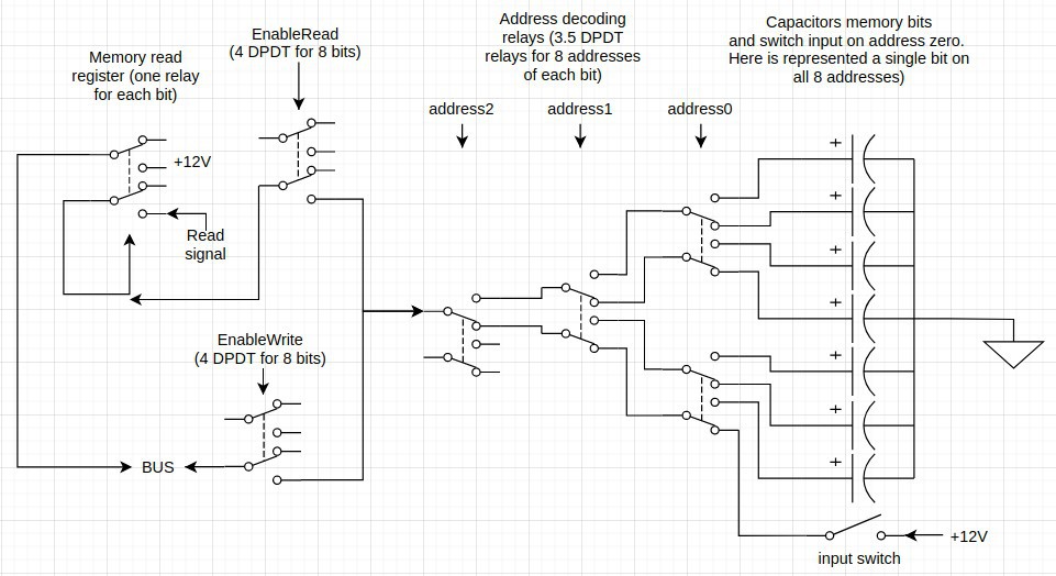
The solution I'm thinking to implement is using just relays and capacitors. Not sure if it is the simplest as I'm always trying to push for, and I'm posting it here also to see if someone can improve it or suggest a new design.
![]()
To write first erase content with EnableRead without Read signal, then switch off EnableRead and switch on EnableWrite and put on the bus what to write.
To read switch on the Read signal than EnableRead will load the Memory read register with the value that is being put on the bus. Release the Read signal when the value is not anymore needed on the bus.
Notes:
1. The data is stored on capacitors, the relays form just the "memory controller" part
2. Reading content "refresh" also the capacitors memory
3. One of the addresses (zero in the example picture) is filled with switches instead of capacitors in order to save one control line and two relays that else should be dedicated to input read
Relays count for 8 bytes (64 bits) memory:
+ 14 relays for address decoding (2+4+8)
+ 2 for EnableRead
+ 2 for EnableWrite
+ 8 for the Memory read register (can be dpdt)
= 18 4pdt + 8 dpdt relays (plus 56 capacitors and 8 switches to complete the circuit!) -
Main unit completed!
12/08/2020 at 16:06 • 6 commentsWith the usual slow but steady speed finally the main module wiring has been completed!
And all functionalities tested worked as expected! There were just a few wiring errors but all of them cought during build time (one wire during the initial two bits test of the ALU, while all the others during immediate recheck of the step work done).
Below the result:
![]()
This is the main unit, missing "just" the random access memory module and the punched tape reader to be a complete system.
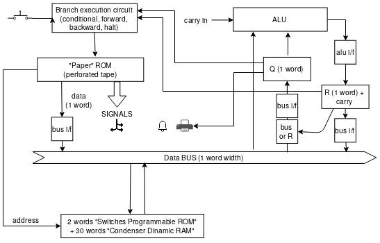
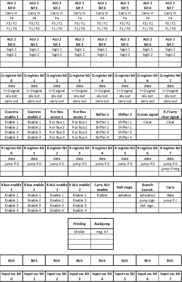
This unit contains: 2 registries, a complete 8 bits ALU with carry bit in and out (able to perform all 16 logic operations, additions, and shifts in both directions), all the bus access interfaces required and the "halt" and "jump" management circuits to control the code flow.
Below some details regarding the implemented halt and branching management circuits (the one for ALU and Q register were detailed also here https://hackaday.io/project/167879-optimized-alus-for-relay-based-computers/log/186329-super-micro-relay-computer-cabling).
BRANCH MANAGEMENT CIRCUIT
![]()
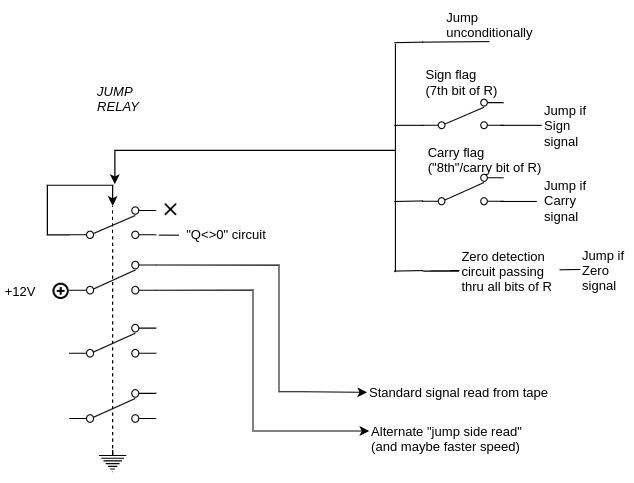
The branch execution circuit is activated when one of the signal of jump "go through" the correspondent condition and activates the jump relay.
Before the jump, Q should be set with the negative value of the numbers of labels to skip, and the circuit stops when Q is zero.
During the jump execution the current is removed from "normal" tape signals and given to a section of tape dedicated to jump instruction where at each label there is:
1. load R with Q+1
2. load Q from RWhen Q will become 0 the signal will automatically go back to the standard instructions side of the tape and instructions signals might also be written "longer" in order to be able to execute at faster tape rotor speed.
Notes
1. jump side signals and standard signals cannot be put on the same "line" since even if not active they might interfere in terms of connections.2. since the number of labels to skip is parametric call/return can be easily implemented (one memory location can be used for the return address) and also indirect jumps are supported by design
3. backward jumps can be transformed into forward jumps if the paper tape is connected in a loop (buth the only forward mechanics should be much easier)
4. to implement a real backward jump another relay should be required to invert the engine poles and to select a second side track that will do Q-1 instead of Q+1 (and with instructions in reverse order since the tape will move backward); this additional switch can be controlled by the higher bit of Q so effectively allowing a -127 to +127 range (instead of the current 1 to 255 labels)HALT CIRCUIT
![]()
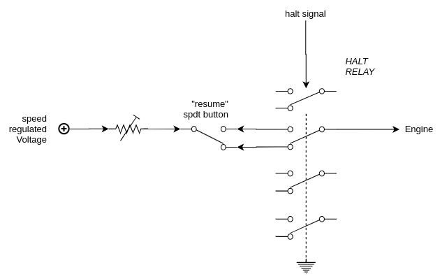
The halt circuitry is optional but very useful since apart at the end of the program can be used for example to input multiple values (or parts of a single larger input) with a cycle:
1. halt (to allow input switches reconfiguration)
2. move switches value to proper memory location
3. go to 1 for the number of times requiredThe configuration avoids that a single keypress skips more than a single halt since the press will advance tape until the halt signal on the tape will stop and to continue the button have to be released.
-
Slow but steady progresses
10/20/2020 at 20:58 • 0 commentsLong time has passed since last post, but things were moving, even if slowly.
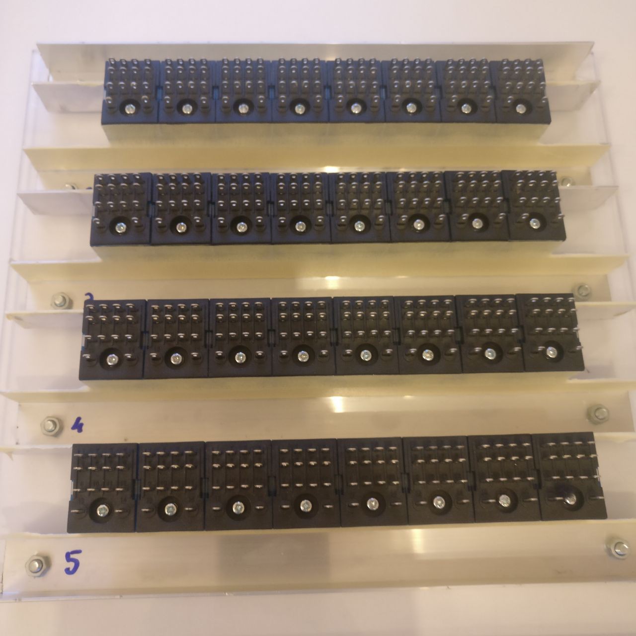
In the meantime I decided to switch to relay socket bases, since faston connections were really too dense to be managed at the scale required.
I also simplified even more the schema avoiding backward jumps: anyway I would not mechanically build them now, and I implemented them as forward jumps on a looped punched tape. This change would be noticeable in nested loops for very long programs but for now there are no plans for that (and in any case I can easily implement it later).
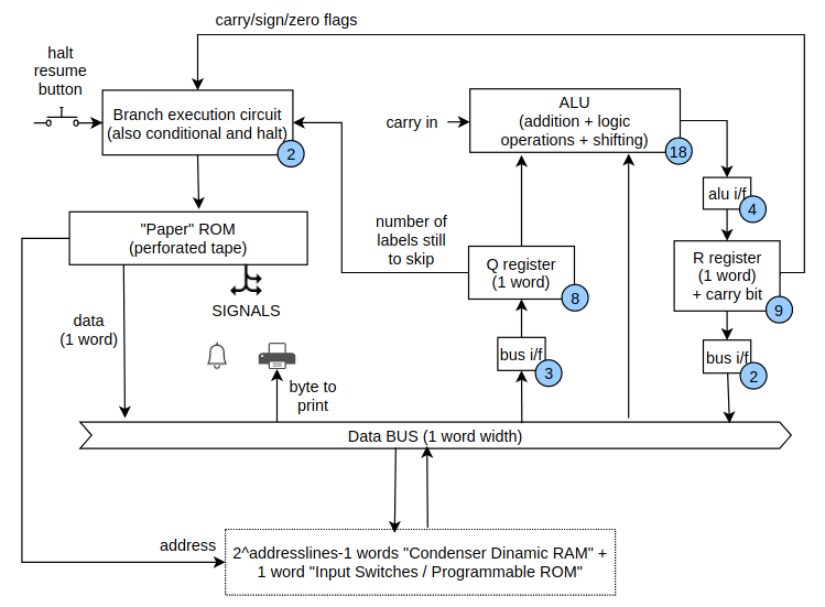
The new schema is as follow (in the azure disks the numbers of relays):
![]()
Totaling for a record 46 relays and nothing else (no resistors, no capacitors, no transistors and no diodes) apart a big mess of wires! :)
The memory design is still open even if I already bought the required capacitors.
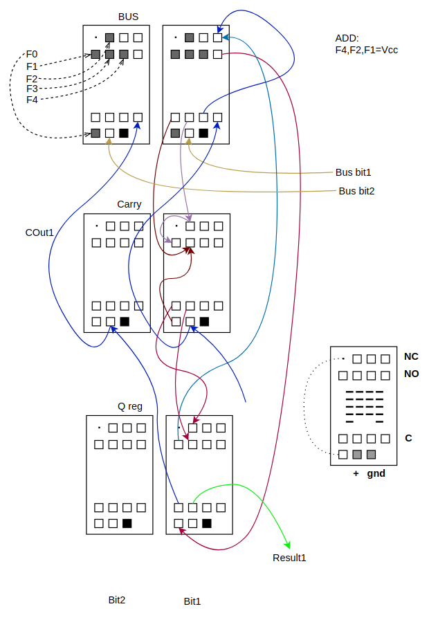
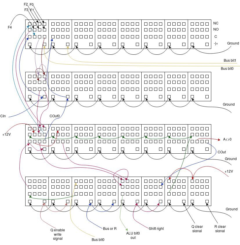
With the bases the ALU needs a new connection cabling schematic (note that since relais are now seen from the top and not from the bottom as before, the bits endianness is increasing from right to left). Below a single bit slice with carry:
![]()
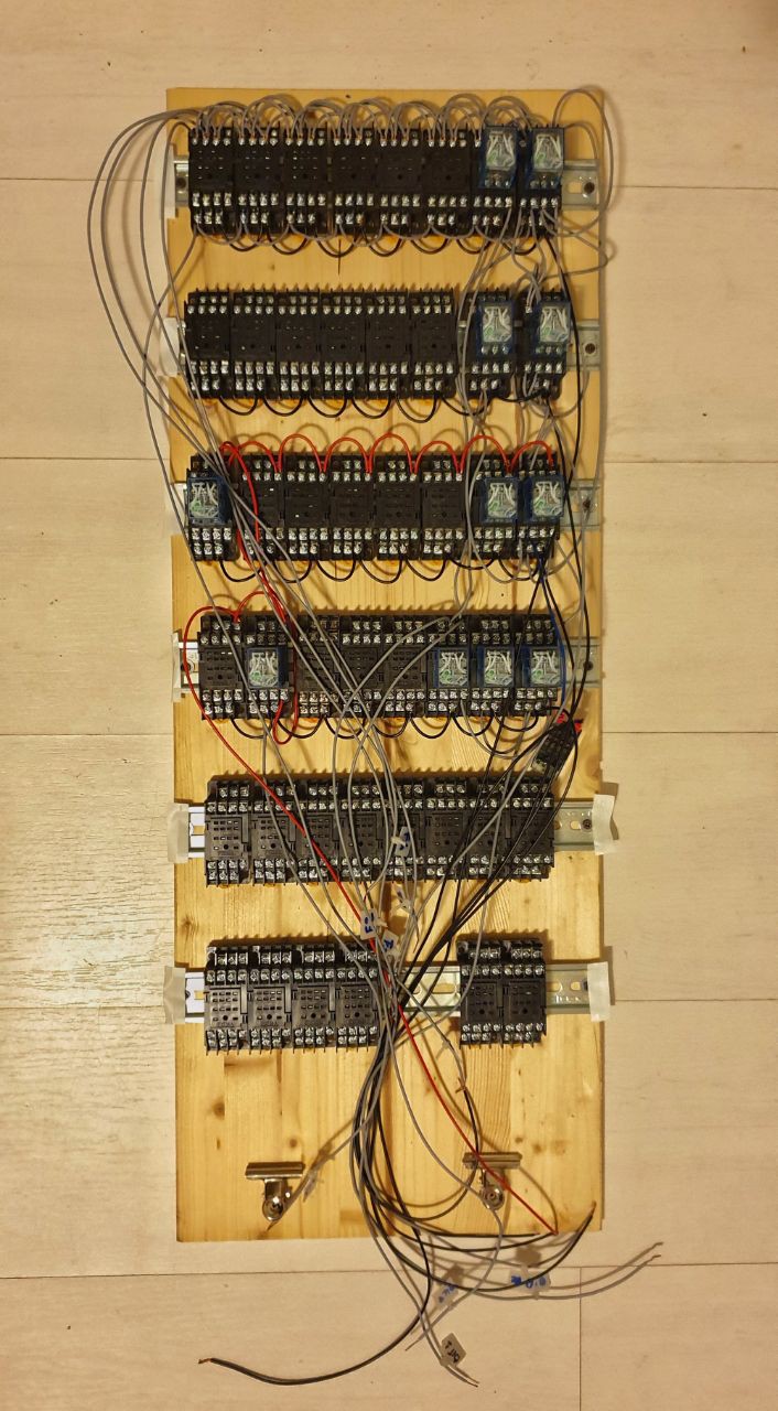
This is the current work in progress:
![]()
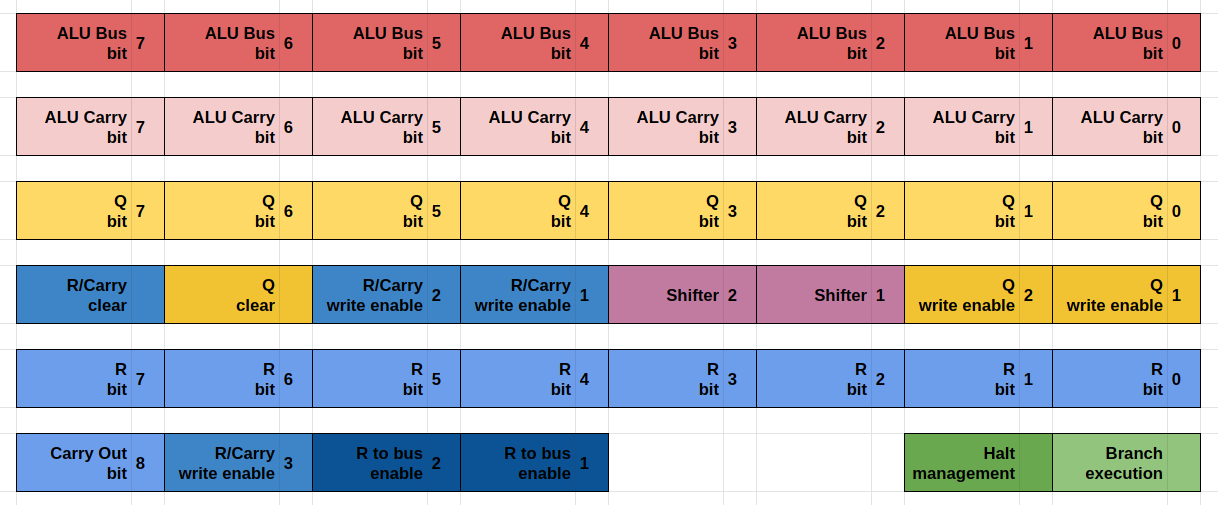
And the relay placement matrix:
![]()
-
Click clack
11/07/2019 at 08:42 • 0 commentsThe good news is: the first bit of the Q register and the ALU have been wired and they're working! Also proving that the more efficient ALU designs are a reality!
I tested for convenience the full adder and for the logic part the NAND operation, but all other logic ones are straightforward to see operating.
![]()
![]()
Below for example 1 of the Q register is added to 1 of the bus and a 1 carry in, resulting in a one on a "flying" bit of the R register and a carry out on second bit (note that relay view is upside down):![]()
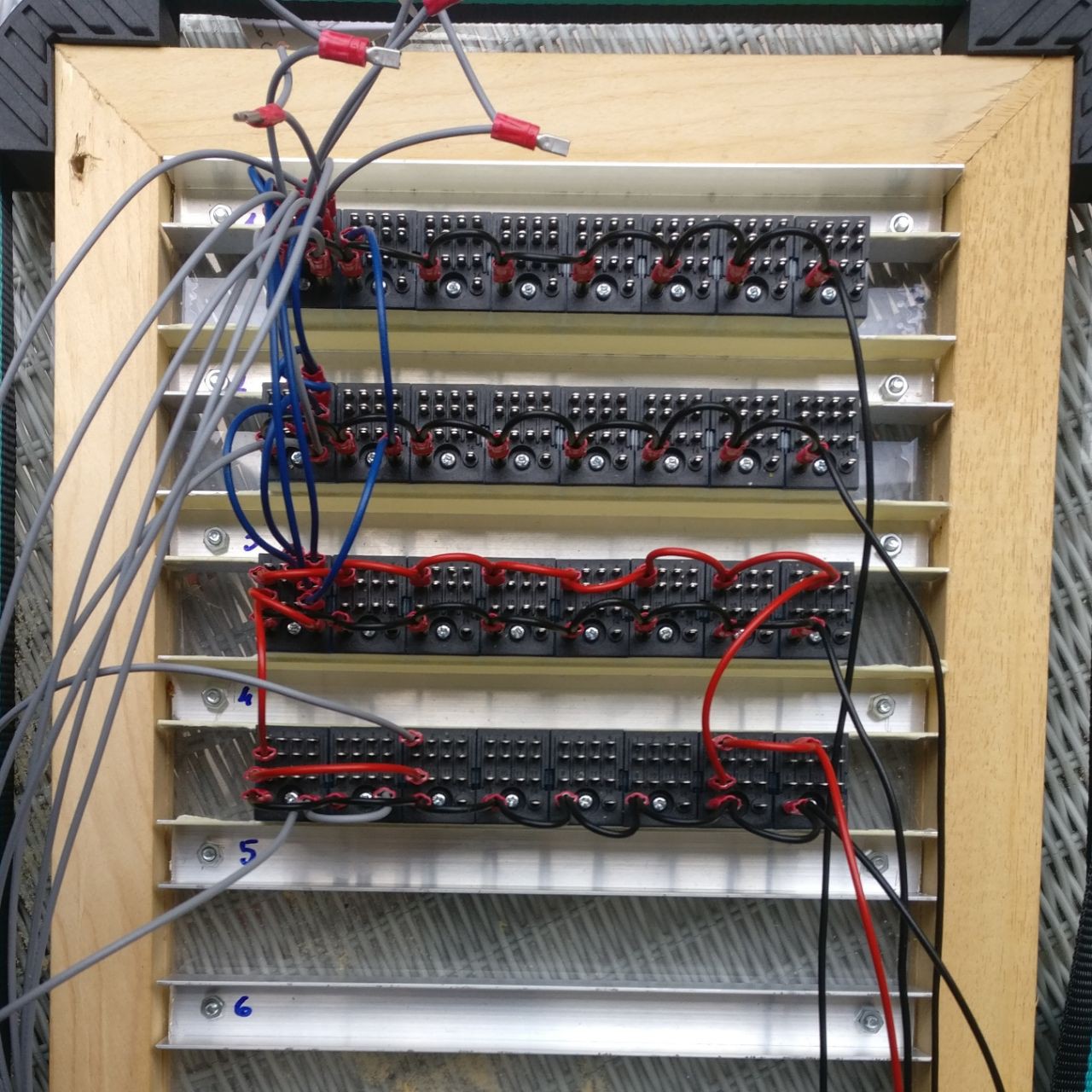
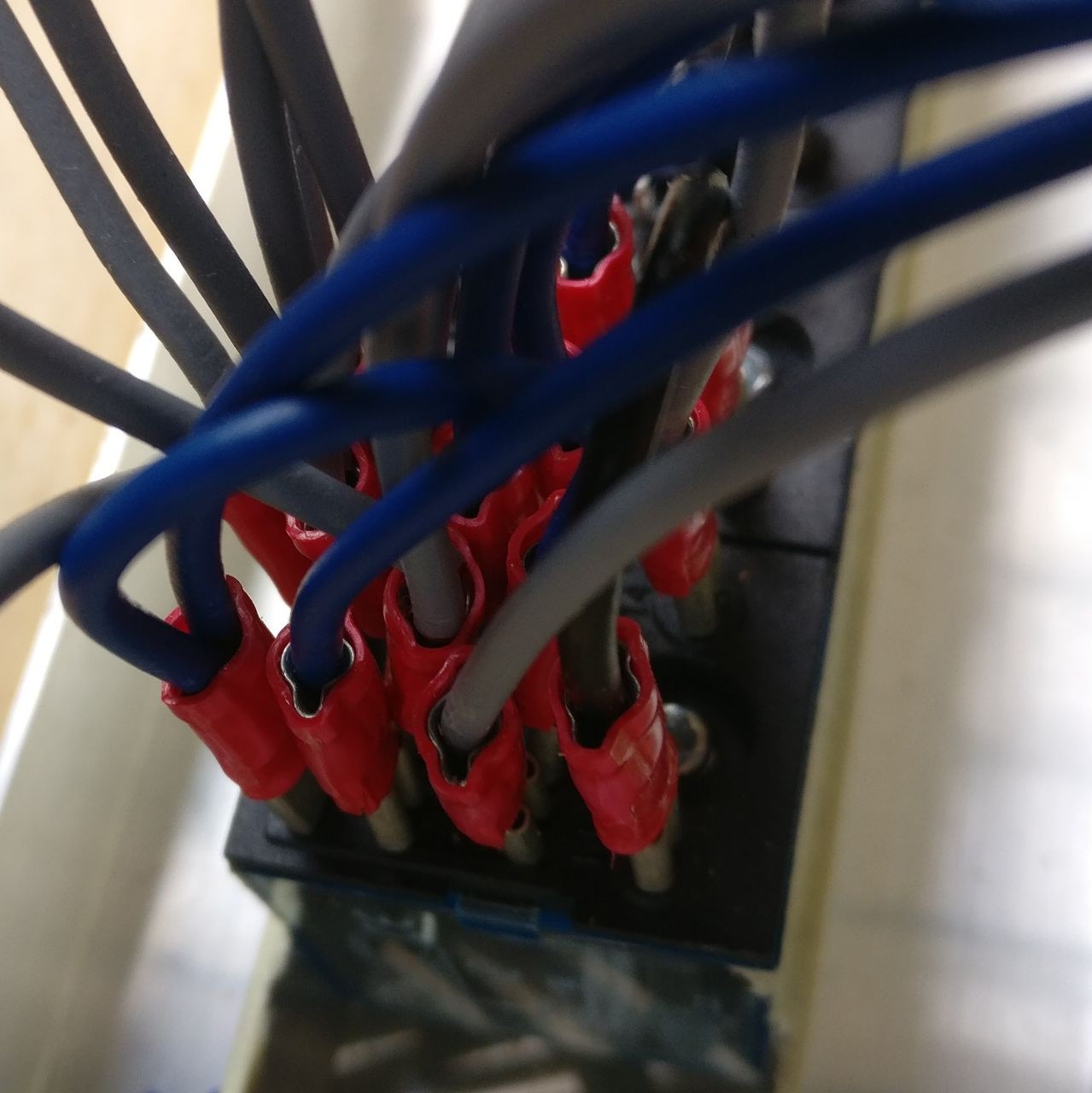
The bad news is that mounting it with fastons as I did is extremely difficult with "dense" relay utilization...![]()
Faston are hard to slot in, and there is very little separation between them with even the risk of a short circuit on the bottom if two adjacent ones are slanted towards each other.
Boefore continuing to mount the rest of the circuit I've to decide how to mount it. Options might be:
1. Continue in this way, maybe finding a way to at least prevent short circuits (e.g. with a plastic foil between adjacent connected row of fastons)
2. Solder the wires to the relays instead of using faston
3. Buy relay bases and "easily" screw the wires (trashing all the effort spent on the frame, adding one month shipping time to the additional money to be spent) -
Planning the layout
10/28/2019 at 20:08 • 0 commentsThe frame start to get populated:
![]()
50 might be a little number of relays but surely is already providing quite an intricate mess of wires and a lot of headaches if not properly planned (and even if properly planned): at least let's try to manage at best!Following a bit more detailed overall schema of the PC (more details of the various circuits will come in later posts):
![]()
And below a tentative to put some order between units in the frame:![]()
As of last image a drawing guide for the wiring of the first bit of the ALU (the famous "no dollars" one of @roelh):
![]()
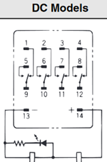
(the full layout of the MY4NJ can be found in first project log)
-
Quality check
10/28/2019 at 07:05 • 0 commentsFirst things first: let's start to see if the relays are properly working...
For the purpose I built a little tester rig:
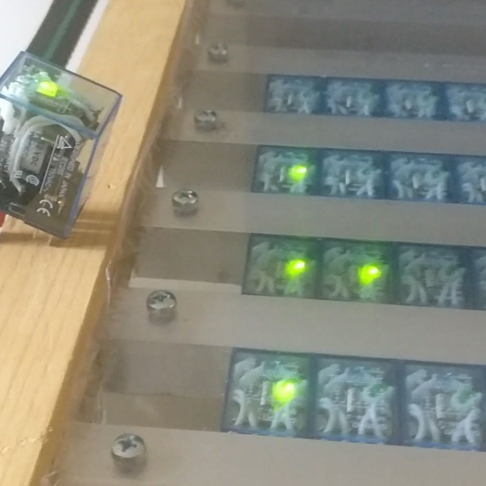
![]() Result? Bad. Out of the 62 relays I've found that 13 of them work unreliably and 3 not working properly at all. Partly good news is anyway that I've 46 remaining that seems working, let's see.
Result? Bad. Out of the 62 relays I've found that 13 of them work unreliably and 3 not working properly at all. Partly good news is anyway that I've 46 remaining that seems working, let's see.
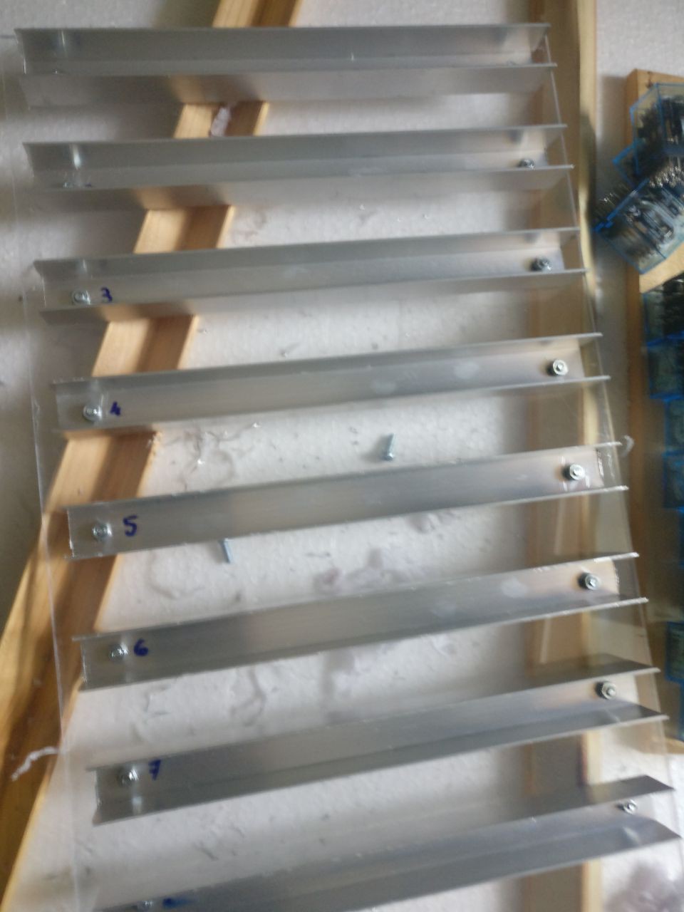
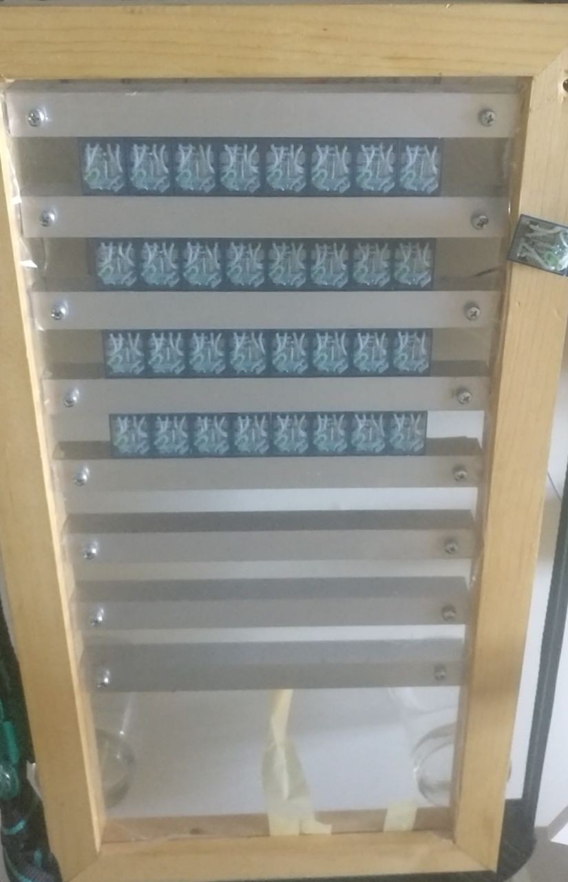
In the meantime I built also a frame to keep the relays of the mounted computer. Here the last assembly step:![]()
-
Let's start!
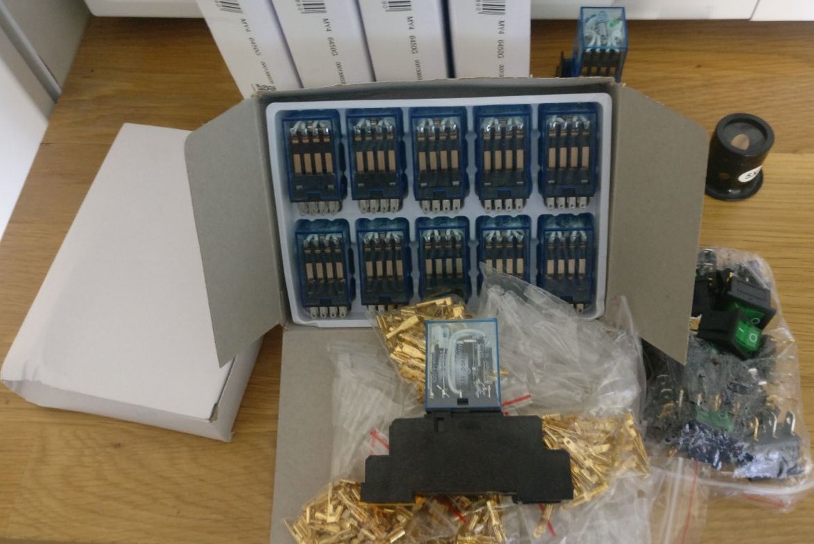
10/20/2019 at 17:33 • 0 commentsRelays finally arrived, and now it's time to start build the computer!
![]()
I was liking transparent relays, where you can see the mechanism moving, and I found them at bargain price online. Buying SPDT, DPDT and 4PDT was practically same amount of money, so I selected all of them 4PDT, that will give also a uniform looking. Moreover 12V DC was the minimum available, and I’ve seen that this is a pretty common choice among other implementations. Looking at them afterwards they seems similar to the Harry Porter’s ones!I bought around 60 of them, hoping even to spare few with 8bit implementation... In reality I might spare even more realizing at least the first version with 4bit word lenght: easier to assemble, to debug, and anyway reaching all goals of the project, and "expanding" it later. I will decide building it. Anyway the design allows for the word to be any multiple of 4bit (e.g. 8, 16, 32 and even 64 bits) since there is no delay accumulation increasing the word size.
The relays number in this moment do not account for the memory. For which I will probaly buy a different type (trough hole) for easyness of assembly with condenser (if the current design will work).
Super Micro Relay Computer
Going back almost 200 years, to what could have been the very early beginning of electronic computing!
 Stefano

 Result? Bad. Out of the 62 relays I've found that 13 of them work unreliably and 3 not working properly at all. Partly good news is anyway that I've 46 remaining that seems working, let's see.