-
TTL radio button for the clock
10/31/2021 at 13:17 • 2 commentsThis new version of the CPU required a new approach for the clock. This is why I thought it would be much easier to use pushbuttons instead of slide switches. That is where the idea of a 4 radio-button style clock selector came from.
There are 4 clock signals to select from:
- Manual
- Variable
- 1Mhz
- 4Mhz
We needed the following features:
- 4 inputs (pushbutton) to select the clock
- 1 reset signal to reset to manual (at startup but also on HALT and BREAK signals)
- 4 LEDS to display the selected clock
- A signal selector to select and output the proper clock signal
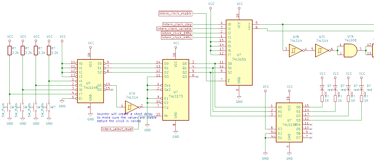
We have selected a combination of 4 elements to perform this task:
- A 74LS148 (8 way priority encoder) that will output 3 bits depending on which pushbutton is pushed and a active-low signal when a pushbutton is pressed. Only the first 4 inputs are used, therefore only 2 bits are required but we still keep 3.
- A 74LS173 (4 bit register) to store which button was selected (3 bits are enough, the 4th one is kept high).
- A 74LS138 (8 bit decoder) used to activate a LED corresponding to the stored entry, again, only 4 outputs are used
- A 74LS151 (8 way multiplexer) to output the selected clock
![]()
So how does it work?
- When pressing a select button on the left, the 3-bit output of the 74LS148 is set to the binary value corresponding the pressed button (0b000 for input 7 to 0b011 for input 4, inputs 3 to 0 are not used). At the same time, the GS signal (active low) is set indicating that a button is being pressed. This signal will be used as a clock for the next step to indicate to store the value of the 3 bits
- The 74LS73 is a 4 bit register, it will store the binary value coming from the 74LS148 presented on its inputs when the clock pulse input is rising (3 bits + 1 value kept low). As the GS signal is active low, we first need to inverse it to get a rising edge instead of a falling edge. This will also create a small delay making sure that the levels of the 3 bits are set before triggering the register. Finally, the master reset input will be used to reset the value to 0b0000 corresponding to the pushbutton 7.
At this step we have a valid binary value stored in the register to represents the current selected channel. We then need to perform 2 tasks:
- Display in a human readable manner the selected channel instead of binary, basically either a Hex display or simply 4 leds, on per input
- Select the clock signal to output
To display the selected channel, we will simply use a 74LS138 (8 output decoder). It will light the proper LED according to the stored value in the register. Note that the outputs of the 74LS138 are active low.
To select the clock, we will use an 8-channel multiplexer (74LS151): based on the binary value inputted on its 3-bit input, it will select and output the right clock channel. Note that there is a side benefit as this chip also provides the inverted signal.
-
New PCBs for the Address Register
11/30/2020 at 18:40 • 0 commentsI finally received, checked, solder and tested the new PCBs for the Address Register.
I built of such registers, one will be the Program Counter and one will be the Stack Pointer and plugged them to the backplane.
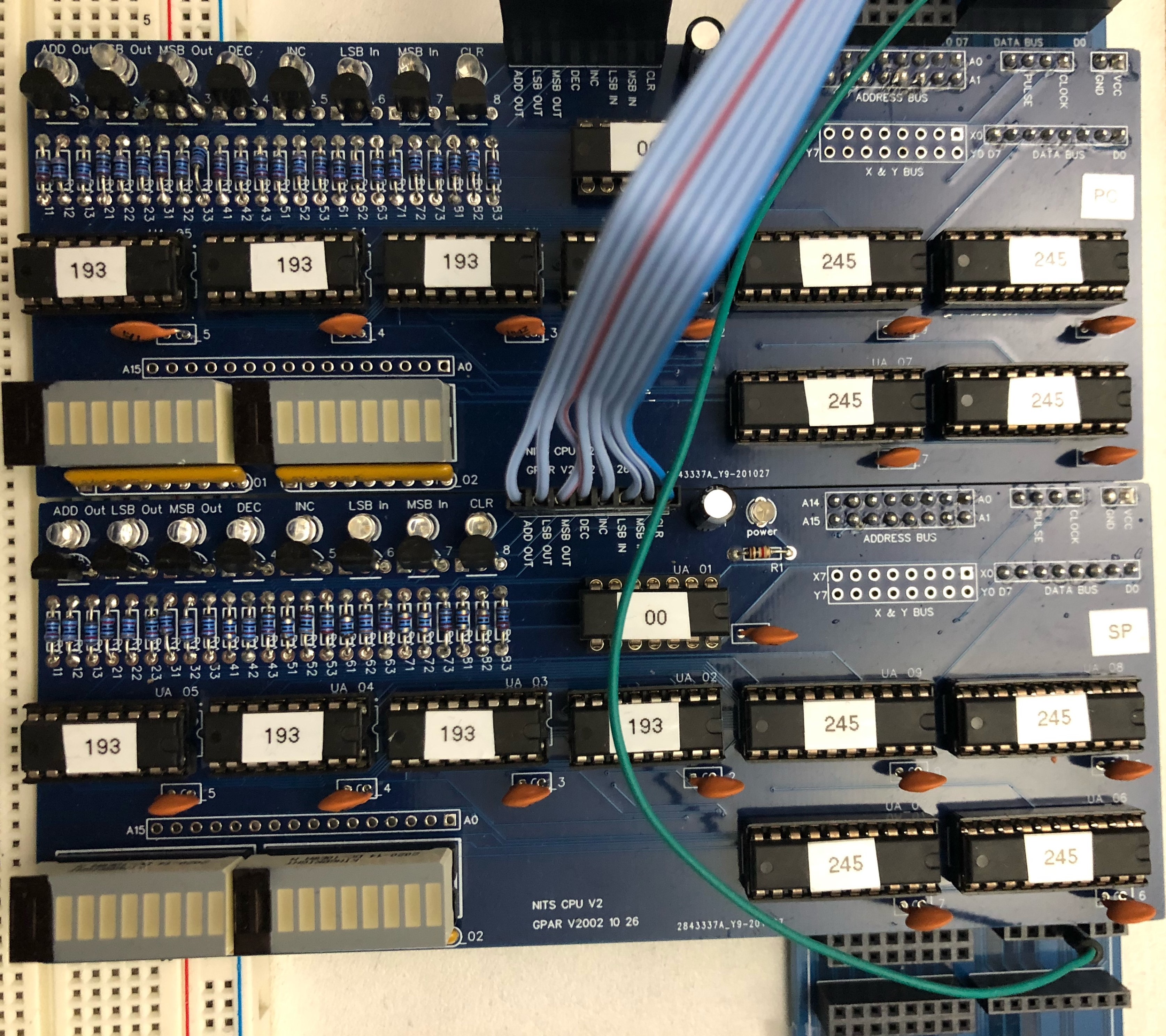
Here is a picture of the two PCB plugged into the backplane with the control lines connected to the arduino (blue cables) for testing purposes. The final Bits CPU V2 will have 2 more such modules for index address registers.
![]()
For more information on the design of the address register, see Testing the Address Register using Arduino.
The next PCBs are already ordered for the Data registers...
-
Measuring propagation delay and look-ahead signal
10/24/2020 at 17:34 • 0 commentsStill working with the GPAR, the General Purpose Address Register. This design includes 4 chained 74HCT193 up/down counters. Each one handles 4 bits and the Adress Register can handle 16-bits in total.
For some operations, the four 193 will work in parrallel, such as the RESET function, or the parrallel load.
But, when using the INCrement or DECrement function, each one has to wait until the previous one is done computing to see if it needs, in turn, to increment or decrement. There is therefore an extended propagation delay for these functions.
Using a 100Mhz digital Logic Analyzer, we are going to measure the delay when using the increment or decrement function. Note that this logic analyser can only sample the signal at 100Mhz, therefore the maximum speed is one sample per 10ns. So the results are not very precise but it can illustrate what is going on.
For this, we plugged the GPAR to a 4Mhz clock, set the DEC function to permanent activation, therefore, the GPAR is decrementing at the speed of the clock, 4 million times per second.
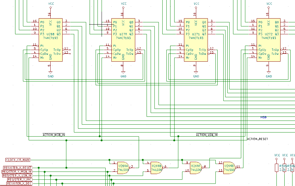
Schematic of the GPAR
The DEC function goes first through a NAND (74HCT00) gate to synchronize with the clock then to the CpDw pin of the first 74HCT193, then each 193 is chained using the special purpose output TcUp and TcDw.
Step 1 - Delay at the NAND gate
Lets look first at the propagation delay of the 74HCT00: the spec sheet says typical t=10ns, max t=25ns.
So lets measure the timing diffence between the clock and the output of the NAND gate. First line is the clock, second line is the NAND out signal.
Here the measure is 10ns (one sample of my analyzer). It's in line with the specs.
Step 2 - Delay to decrement the first 193
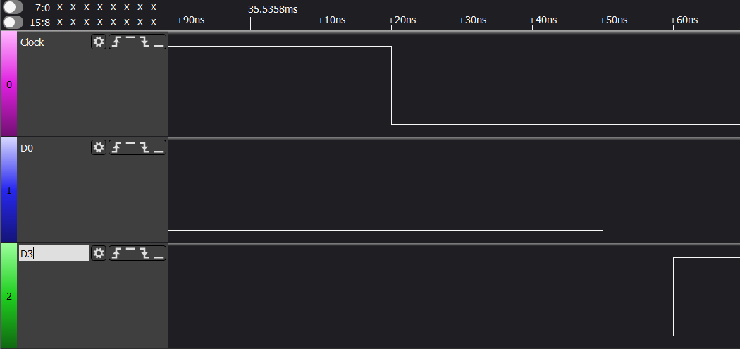
So now we measure the time it takes to decrement the value of the first counter. We select a specific moment, when both the first bit (D0) and the last bit (D3) of the counter switch (the counter decrements from 0b0000 to 0b1111)
The propagation delay is measured at 30ns from the clock signal, so lets say 20ns from the NAND out signal for the first bit and 40ns for the last one, this is consistent with the specifications of the 74HCT193:
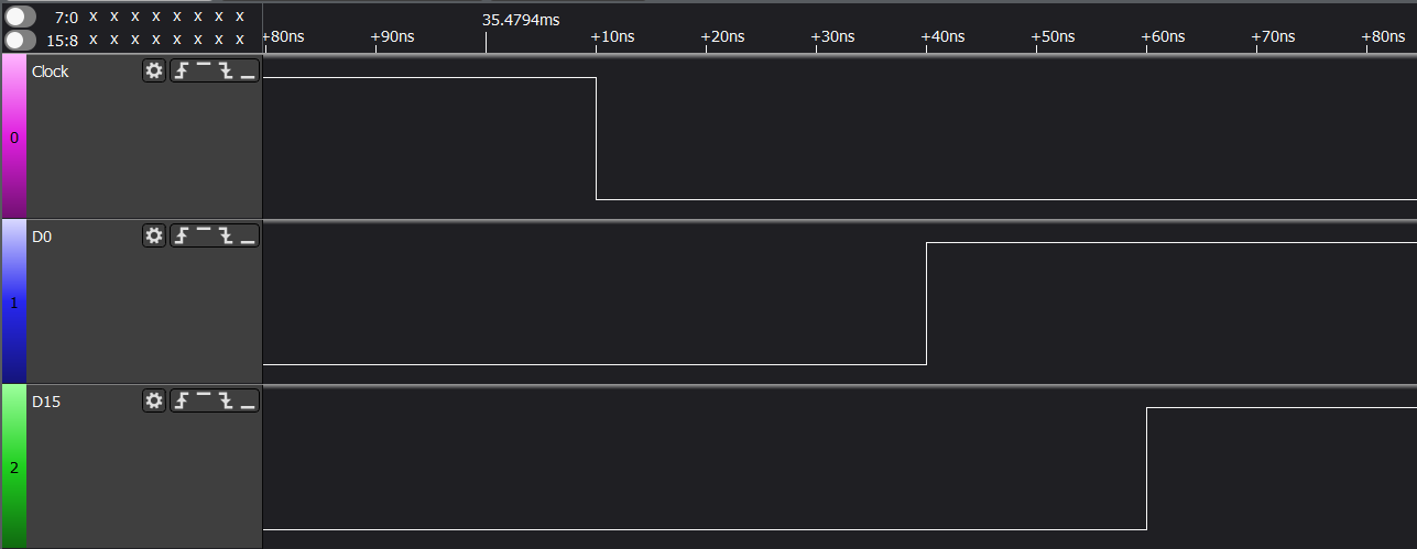
Step 3 - Delay to decrement all counters
For this final measure, we consider the worst case scenario where all counters need to decrement. We measure the difference between the clock, the first bit of the first counter (D0) and the last bit of the last counter (D15):
We can see the same propagation delay for the first bit D0, but considerably more for the last bit D15:
- Delay for the first bit: 30ns minus the NAND 10ns = 20ns
- Delay for the last bit : 60ns minus the NAND 10ns = 60ns
However, this is strange because how could decrement over 4 chained counters take only 40ns (60ns delay for the last D15 minus 20ns delay for the first D0) when one counter by itself takes 20ns?
The great trick of the 74HCT193
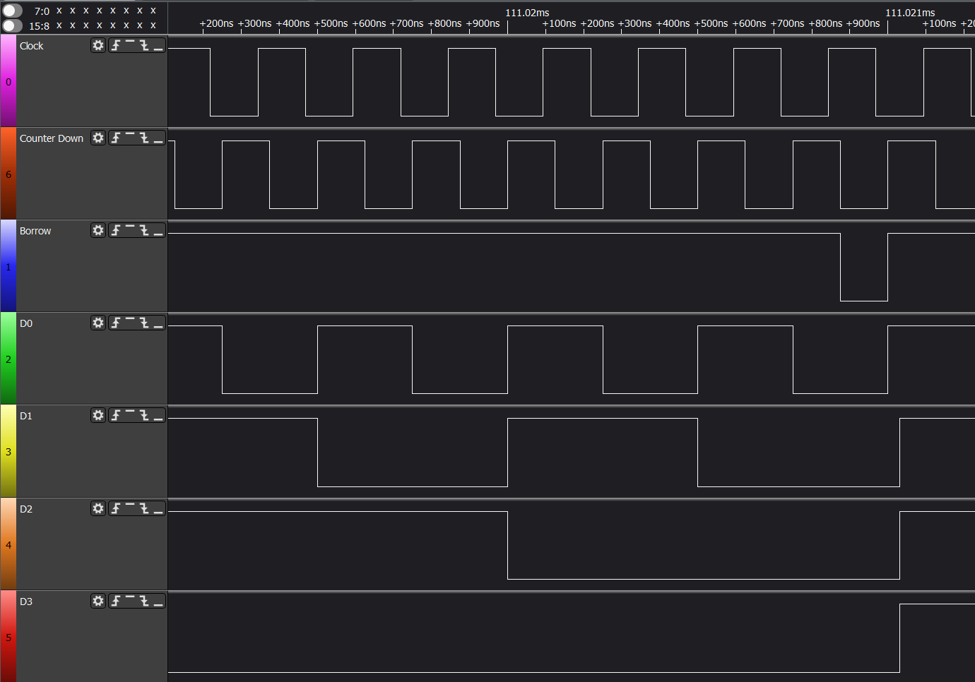
Well this great IC has a trick, it doesn't compute the result of the counting to consider sending a carry signal or a borrow signal to its neighbour. It already know before the computation that it will not be able to perform the compute by itself and sends the signal immediatly. This is called the look-ahead carry or borrow. Basically:
- If the chip value is 0b0000 and we want to decrement, it can send the borrow signal immediately
- If the chip value is 0b1111 and we want to increment, it can send the carry signal immediately
Here is a clear measurement of this features (remember we are decrementing so it is a borrow signal). Look at the area where all the values D0 to D3 are at 0, we can see that the borrow signal mimics the decrement signal. For all the other values of D0-D3, the borrow signal stays high.
-
Testing the Address Register using Arduino
10/11/2020 at 18:10 • 0 commentsWhile still working on updating the PCBs and fixing some bugs for the build, I started wondering how to massively test the modules (breadboard or pcb) and of course the Arduino came handy.
The General Purpose Address Register (GPAR) is described in this blog post. It provides a 16-bit wide address register, reset, increment and decrement functions and can publish its values to both the Adress Bus and the Data Bus.
To test the features we will need to check each functions:
- Capability to move a 16 bit value to the register using the Data Bus (The Data Bus is only 8-bit wide, therefore we need two steps, moving the MSB-Most Significant Byte and then the LSB-Less Significant Byte)
- Capability to retrieve a 16 bit value from the register using the Data Bus (same)
- Capability to increment the value stored in the register
- Capability to decrement the value stored in the register
- Reset
The program must also make sur that the cabling is ok (either within the prototype or between the arduino and the prototype). For this we will light up all the LEDs slowly one by one in a specific order for a visual check.
The program does the following:
- Check each action signal by lighting the appropriate LED, this will enable checking the wiring between the arduino and the prototype and the LED capability (8 signals total)
- Check each register bit by uploading the appropriate value (0, 1, 2, 4, 8, etc) to the register. Each time, the given led should light up. This will again ensure the cabling between the arduino and the prototype is correct and that the inner workings of the register are ok
- Generate random number between 0 and 65535 and perform the following (many times)
- Move the value to the register (2 steps)
- Retrieve the value from the register and compare it (2 steps, retrieved value should be identical)
- perform an increment (1 step)
- Retrieve the value from the register and compare it with the locally incremented value(2 steps, retrieved value should be identical)
- Perform a decrement (1 step)
- Retrieve the value from the register and compare it (2 steps, retrieved value should be identical to original value)
- Perform a Reset (1 step)
- Retrieve the value from the register and compare it to 0 (2 steps)
The artduino will stop if an inconsistency between what is retrieved and what is expected is found.
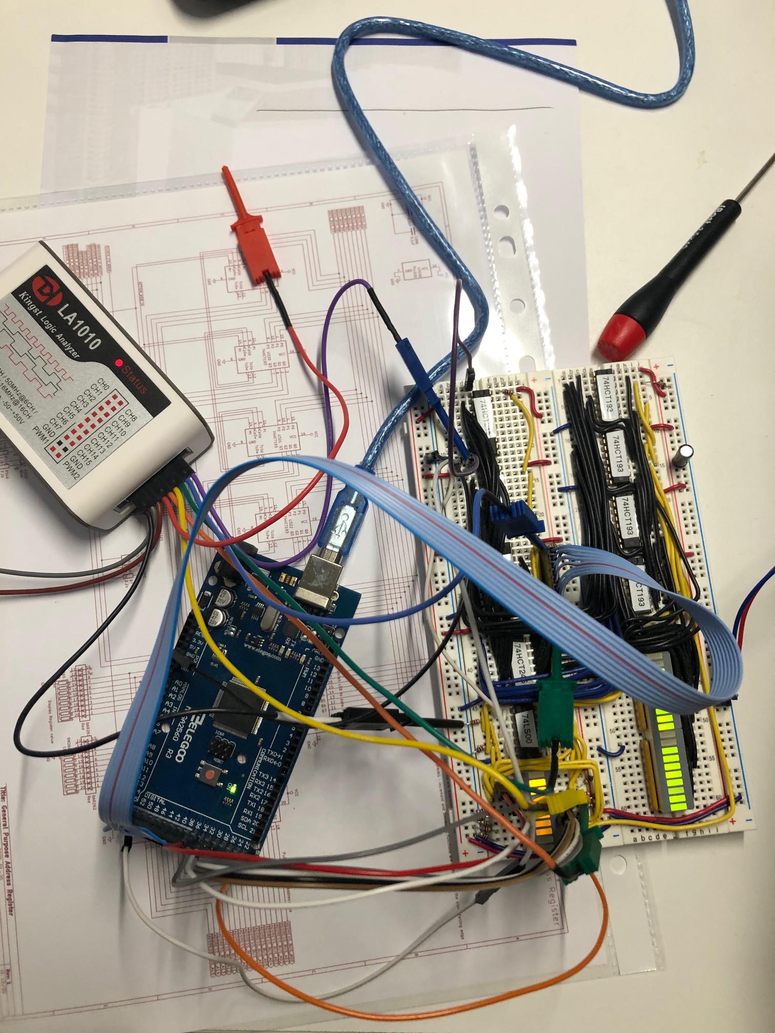
![GPAR being tested by the Arduino and measured GPAR being tested by the Arduino and measured]()
This photo shows:
- The GPAR prototype on two breadboards using mainly 74xx193 and 74xx245
- the arduino mega used to perform the tests
- A logic analyser to measure the frequencies
The outcome is very positive from the features perspective : everything performs as expected.
However, it must be said that the arduino is quite slow and that the maximum test frequency is 9Khz, very far from the target in the Mhz area.
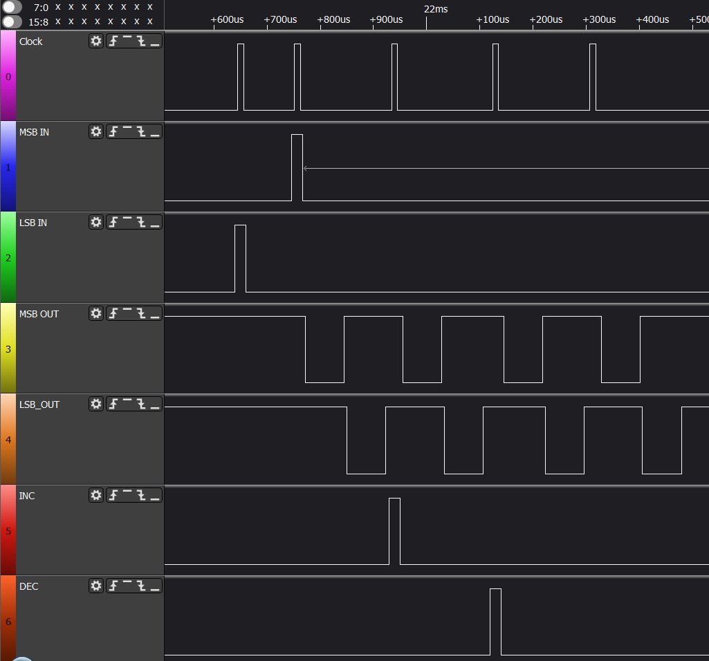
Here is a full cycle of tests:
- Line 1 is the clock
- Line 2 and 3 are the MSB_IN and LSB_IN signals enabling the move of 2 bytes as 1 16-bit value into the register
- Line 3 and 4 are MSB_OUT and LSB_OUT (active low) enabling the retrieval of the 16-bit value stored in the register as 2 bytes
- Line 5 is the increment signal
- Line 6 is the decrement signal
- The reset signal is not displayed
Unexpected issue
The address register is supposed to strictly work between the address x0000 and xFFFF, therefore the is no overflow detection. Therefore when the arduino program generated a value such as xFFFF, it was then incremented to become x0000 (no overflow), and then decremented and it stayed at x0000. Of course, the arduino flagged this as an error. The program was fixed to ignore this issue and consider the value ok.
-
First PCBs
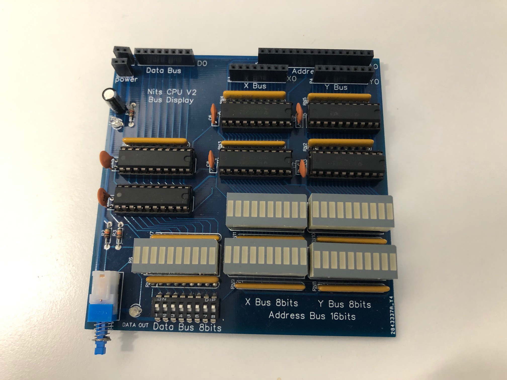
06/07/2020 at 11:46 • 3 commentsThe first PCB I wanted to create was dedicated to displaying all the Buses and provide the capability to publish a value to the Data Bus. A helpfull debugging tool.
This module provides the following:
- Display the 8-bit X Bus
- Display the 8-bit Y Bus
- Display the 16-bit Address Bus
- Display the 8-bit Data bus
- Publish a manual value, set using dip switches to the 8-bit Data bus
In order to minimize impact on the buses when plugging the module all the LEDs are driven by a 74LS245 bus driver.
![]()
The PCB is dual sided, ordered from a well known provider.
The switch enables the publishing of the Data bus value. No switch debouncing is needed on this test board. It works perfectly.
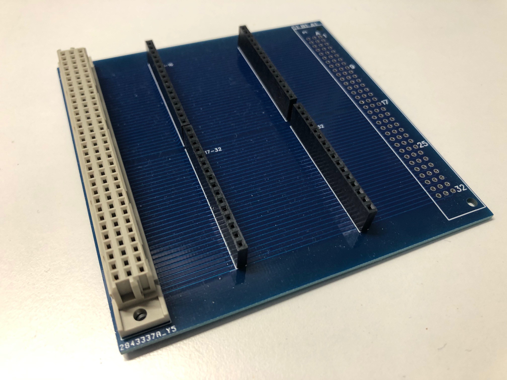
The second PCB, also for test purposes is a simple 41612 64 pin connector facilitator. It enables easy access to any pin of the connector to use a dupont-cable.
![]()
I built 2 of thoses, on for the female 41612 connector (seen here), one for the male version (just solder a male connector on the right side of the PCB instead) in order to also test the backplane.
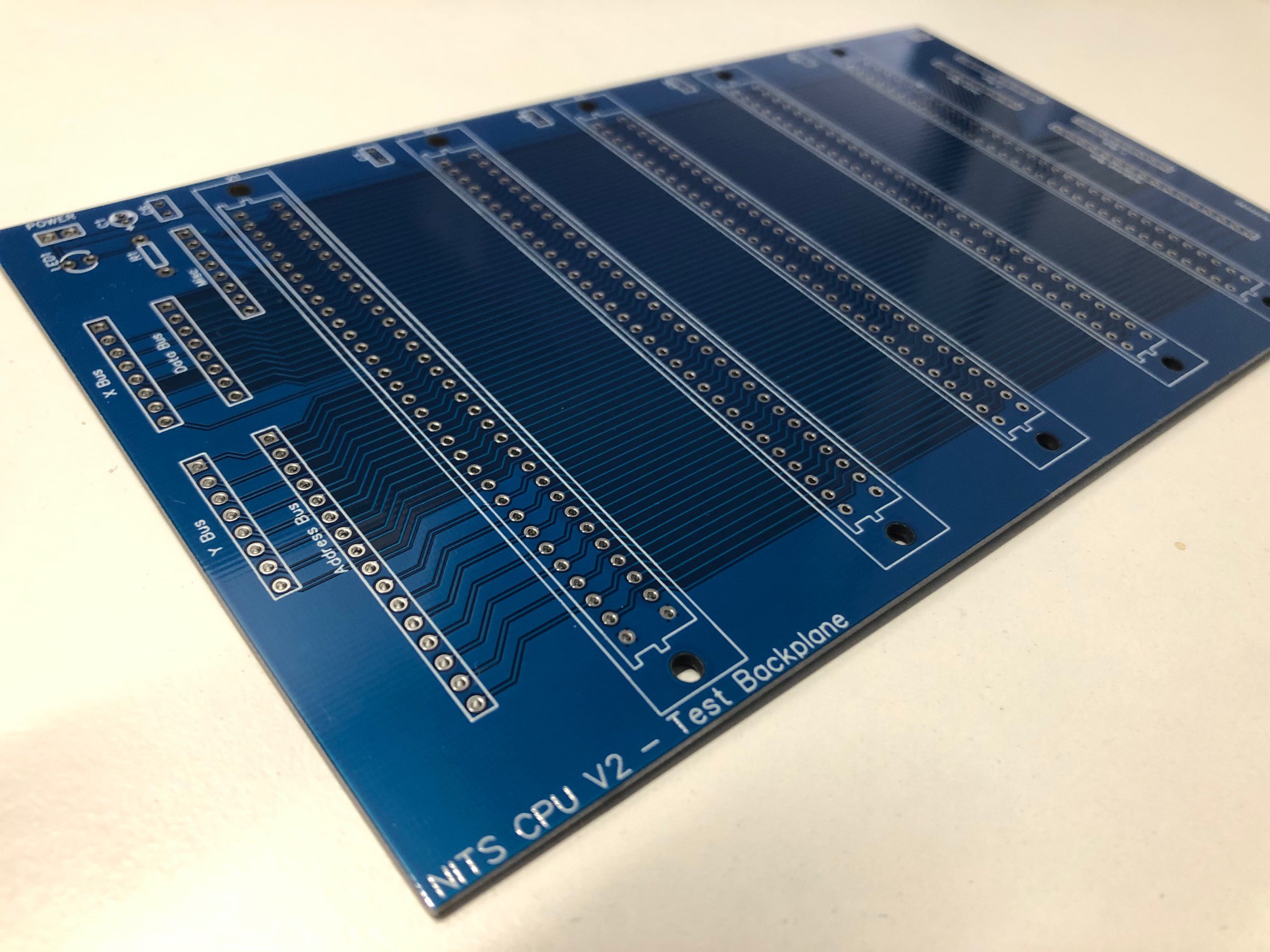
Here is a preview of the test backplane (connectors not installed). It provide 5 41612 connectors, power supply, decoupling caps, and direct access to some buses (to be used by the bus display above).
![]()
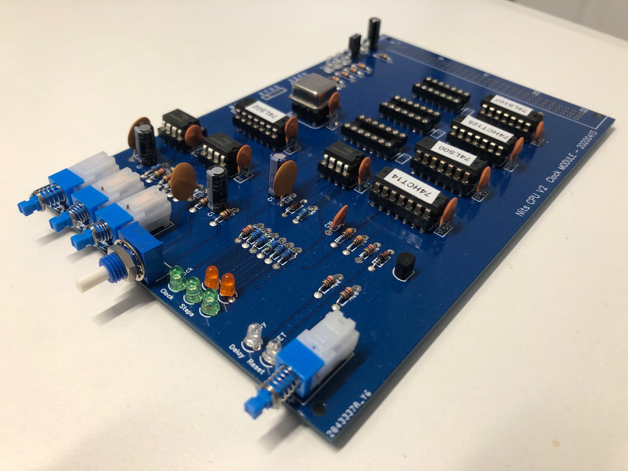
Finally, my big error in design, I built a PCB for the final version of the clock module, quite a complex PCB for my level of expertise and I messed up one chip (used a NOR instead of an OR gate and the pinouts are not compatible). So this is the partially built version. I stopped when I found the error.
![]()
It was supposed to have an 41612 connector, get power from the baclplane and provide reset and clock to the backplane. I will therefore need to design a second version.
Until the redesign, I will hack this one to make sur the updated design fixes the errors.
-
Prototype of the new Address Register
04/15/2020 at 08:47 • 0 commentsThis post is a followup of the Improved Address Register post.
We have identified 4 asynchronous actions:
- Publish MSB to data bus: -msb-out, asynchrounous
- Publish LSB to data bus : -lsb-out, asynchrounous
- Publish value to Adress bus : -add-out, asynchrounous
- Clear value (reset) : -clear, asynchrounous
and 4 synchronous actions:
- load MSB from data bus : -msb-in, on clock rising edge
- load LSB from data bus : -lsb-in, on clock rising edge
- Increment value : -inc, on clock falling edge (see note)
- decrement value : -dec, on clock falling edge (see note)
However, the 74HCT193 does not provide a clock entry, therefore it has to be built with an NAND gate to synchronise the action signal and the clock. So when activating the INC action, NANDed with the clock, will provide a HIGH-LOW-HIGH transition synchronous with the clock.
NOTE : the 74HCT193 has a strange behaviour in a way : it needs the clock inputs to be HIGH to count, but it counts on the rising edge. So, in order for intance to have a count UP you will need :
- CPDw to be HIGH
- CPUp which was HIGH to first go LOW and then go HIGH.
This means that the couting will not take place on the clock rising edge but on the clock falling edge after the NAND gate.
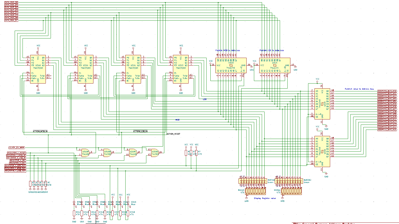
The 4 NAND gates provides 4 clock-synchronous action signals to control the 74HCT193. We need 4 of these to provide 16 bits. The increment and decrement counters are daisy chained to provide the counting capability :
The reset pin (Mr in the diagram) is just the same signal for all four chips.
The Pl (parallel load) signal is however distinct because we need to be able to load either the lower 8 bits (LSB) or upper 8 bits (MSB).
Therefore the output of the NAND gate for the signal REGISTER_X_MSB_IN is routed to the Pl pin of the two left chips and the output of the NAND gate for the signal REGISTER_X_LSB_IN is routed to the Pl pin of the two right chips.
Finally, for the output, we need to :
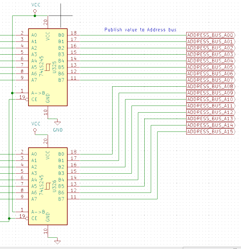
- publish the full address (16 bits) to the address bus. This is done using two 74HCT245 bus drivers with only one publish signal connected to both REGISTER_X_ADD_OUT (active low):
- publish the upper 8 bits to the data bus. This is done using one 74HCT245 bus driver driven by the REGISTER_X_MSB_OUT (active low) signal
- publish the lower 8 bits to the data bus. This is done using one 74HCT245 bus driver driven by the REGISTER_X_LSB_OUT (active low) signal
Overall, there are 9 chips to perform all these features:In this diagram we added:
- 2 LED bargraphs to display the current value of the register
- 8 pullup/pulldown resistors to ensure that even if not connected the actions signals do not perform any action
- 8 signal LEDs to display the action sigals
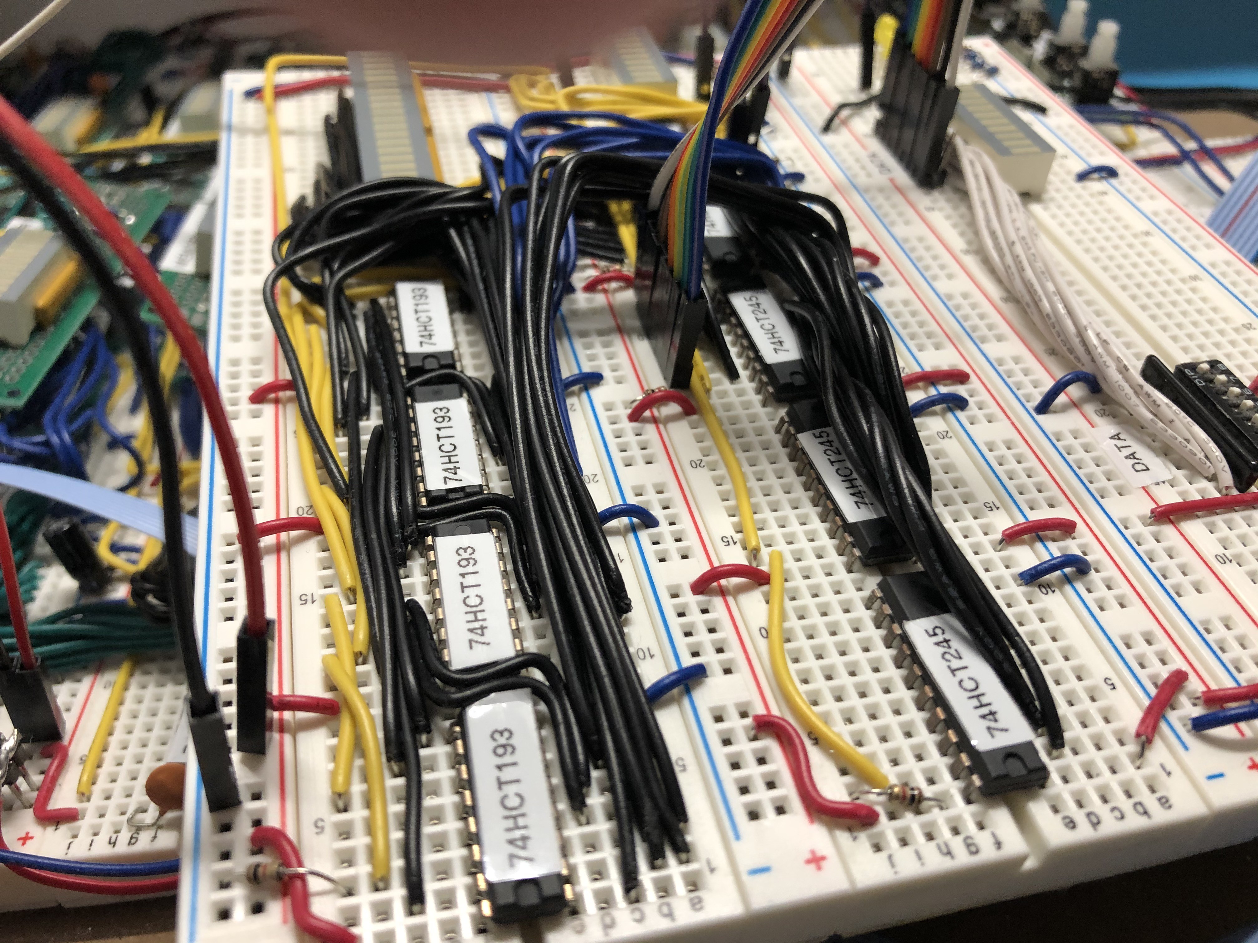
Here is the prototype using breadboards. It's a bit messy because the 74HCT193 have a very weird pinout.
![]()
The prototype has been tested and is working perfectly. Max tested frequency is 4 Mhz.
The next step is to build a PCB for this Register and connect it to a bus backplane. We will need 4 of these.
-
Improved Address Registers
01/20/2020 at 15:28 • 0 commentsOur current CPU has many limitations, including on the register level. This post will look at how to improve the registers that handle memory or output addresses.
First, let's look at the current register capabilities:
- there are basically only two memory address registers : the Program Counter (PC) and the Memory Address Register MAR)
- these registers are 8-bit registers, therefore they can only address 256 bytes of memory or IO
- Only one provides the increment capability (the Program Counter) however it cannot directly address the memory and has to go through the MAR (memory address register)
- None can decrement
- There is no stack pointer
- There is no index register
So lets try to design a single General Purpose Address Register (GPAR) that would provide:
- 16 bits in order to address 64k words of memory space
- increment and decrement capability in order to serve also as PC (Program Counter) and SP (Stack Pointer) without the need of the ALU
- Read and Write capability from the databus which is only 8-bit, in order to access both MSB (Most Significant Byte, the byte of higher value of the 16-bits) and LSB (Least Significant Byte, the byte of lower value of the 16-bit)
- Write capability to the 16-bit address bus
Now what type of instruction these registers should be able to handle :
- LD PC-MSB, D2 : meanind load the MSB of the PC address register with the content of register D2
- LD D2, IX-LSB : meaning load D2 with the content of the LSB of the index pointer IX
- LD IX-LSB, IY-MSB : meaning load the LSB part of ix with the content of the MCB part of IY
- INC IX
This shows that at any given time, it must be possible to output any of the content of any part of the register ***AND*** input any other part of any other register.
Possibly even within the same register:
- LD IX-MSB, IX-LSB: meaning loar the the MSB part of IX with the LSB value of IX
We therefore need to separate the output action functions from the input action functions.
For output and reset:
- Publish MSB to data bus: -msb-out, asynchrounous
- Publish LSB to data bus : -lsb-out, asynchrounous
- Publish value to Adress bus : -add-out, asynchrounous
- Clear value : -clear, asynchrounous
For input and other:
- load MSB from data bus : -msb-in, on clock rising edge
- load LSB from data bus : -lsb-in, on clock rising edge
- Increment value : -inc, on clock rising edge
- decrement value : -dec, on clock rising edge
In the end we need:
- 3 bits to select the output register (value 0b000 serves as not selected)
- 2 bits to select the output/reset function (MSB, LSB, address bus or reset)
- 3 bits to select the input register (value 0b000 servers as not selected)
- 2 bits to select the input/other function (input MSB, input LSB, inc, dec)
With a total of 10 bits, we can perform any type of function on the General Purpose Address Registers.
Here is the naming convention for the register select bits:
- None: code 0b000
- Program Counter : PC, code 0b001
- Stack Pointer : SP, code 0b010
- Index Pointer 1 : IX, code 0b011
- Index Pointer 2 : IY, code 0b100
Here is the convention for the output action (all are asynchronous):
- Publish MSB to data bus: -msb-out, code 0b00
- Publish LSB to data bus: -lsb-out, code 0b01
- Publish value to Adress bus : -add-out, code 0b10
- Clear value : -clear, code 0b11
Here is the convention for the input/other functions (all are on the clock rising edge):
- load MSB from data bus: -msb-in, code 0b00
- load LSB from data bus: -lsb-in, code 0b01
- Increment value : -inc, code 0b10
- decrement value : -dec, code 0b11
Lets now review what the 10 bits would be for the instructions listed above:
- LD PC-MSB, D2
- select output register NONE: 0b000 (D2 is not consider as we are focusing on the GPAR only)
- select output function X : 0b0
- select input register PC : 0b001
- select input function -msb-in: 0b00
- Result is : 0b000000100
- LD D2, IX-LSB
- select output register IX: 0b011
- select output function -lsb-out: 0b0
- select input register NONE : 0b000
- select input function X: 0b00
- Result is : 0b011000000
- LD IX-LSB, IY-MSB
- select output register IY: 0b100
- select output function -msb-out: 0b1
- select input register IX : 0b011
- select input function -lsb-in: 0b01
- Result is : 0b100101101
- INC IX
- select output register NONE: 0b000
- select output function X: 0b0
- select input register IX : 0b011
- select input function -inc: 0b10
- Result is : 0b000001110
- LD IX-MSB, IX-LSB
- select output register IX: 0b011
- select output function -lsb-out: 0b0
- select input register IX : 0b011
- select input function -msb-in: 0b00
- Result is : 0b011001100
So what do we need to build such a register ?
- capability to store value
- capability to reset value
- capability to increment value
- capability to decrement value
- capability to scale up to 16 bits (including on the increment and decrement value)
- capability to select where to publish all (such as the full address) or part (such as the MSB) to a bus, with 3-state outputs
This can be built using 2 types of ICs:
- the 74HCT193 which is a binary 4-bit up/down cascadable counter, prestable, with reset. We will need 4 to store the 16 bit address
- the 74HCT245 wich is an octal, 3-state transceiver. We will need 4:
- 2 to publish the 16 bits to the address bus
- 1 to publish the MSB to the data bus
- 1 to publish the LSB to the data bus
As usual, LED bargraph will be used to display the current value of the counter. We will be be using 470ohm current limiting resistors to reduce the power consumption if the register.
Finaly, there is a need for decoding the actions signals:
- Two 74HCT138 will decode the register select value. Output Y0 is used to perform nothing, Y1 to Y4 to select which register, and it can be expanded to 3 more
- A bunch og logic gates to build the proper signal
Note that 4 actions need to be synchronized with the clock.
More to come soon on this topic.
-
What next?
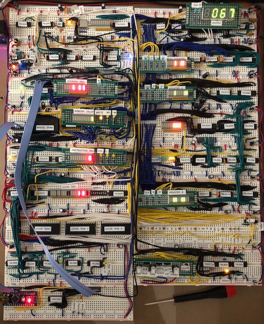
01/14/2020 at 10:23 • 0 commentsThe first version of the Nits Processor is now finished. It is turing complete with a very basic set of instructions, it is possible to upload a program and run it, it can display a result on the 7-segment display.
Here are a few photos.
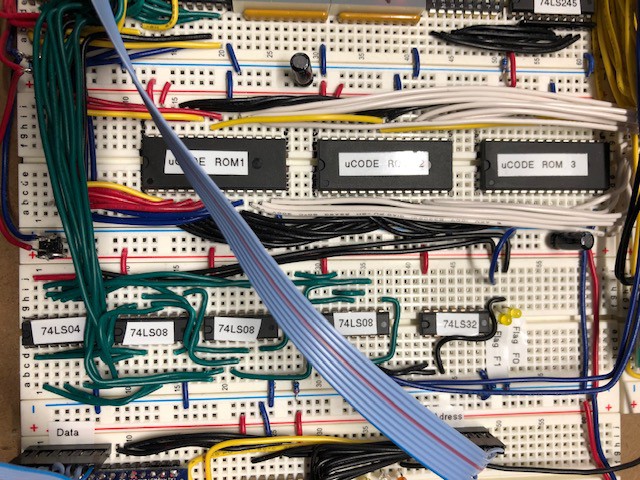
The instruction decoder (3 EEPROMS for 17 signals and a set of gates to decode the flags):
![]()
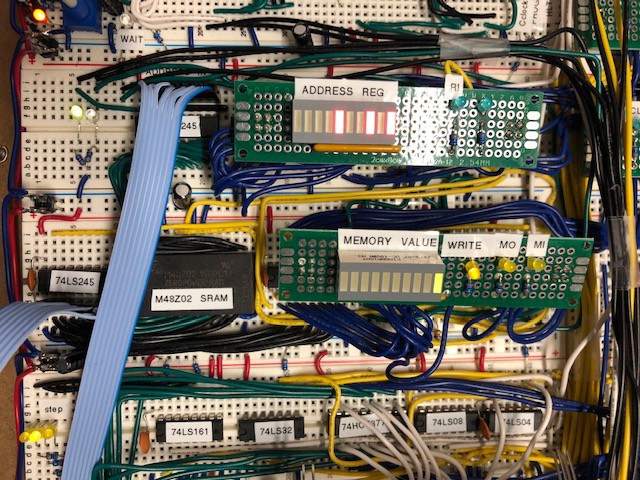
The memory (256 bytes stored in Non Volatile Static RAM, with the Address Register, the memory value display).
![]()
The two flat cables come from the memory loader module (Arduino based). One is the Address bus and one is the data bus. They are used in PROG mode to upload the program to the memory.
It is now time to think about the next steps. What are the current limitations and how can it be improved.Improvements can be of 3 sorts:
- Improve the instrution set
- Improve the architecture
- Improve the build
Improve the instruction set
The instruction set is very limited and really needs to be expanded to provide usable capabilities. For instance:
- Add basic logic functions (And, Or, Not, Exclusive or)
- Add shift functions (Shift, Shift Circular, Shift with carry)
- Add compare functions (zero, equal, greater than)
- Add Push and Pop capability (requires a dedicated stack pointer register)
- Add Call and Return
- Add bit management (test flags, store flags, bit operations)
Improve the architecture
With only 2 registers, the lack of stack pointer and only 256 bytes of memory for both data and program, the current archietcture can really be improved:
- Expand address bus to 16 bit (hence 64 Kbytes of memory). However this requires many changes because now the address bus can be double the size of the databus and ALU creating a challenge when computing addresses
- Expand the number of registers, at least to 4 General Purpuse Registers
- Separate memory from Input-Output. This will provide double the addressing capability
- Add a way to interact with the system, for instance with a proper serial interface
- add a ROM with basic functions including initial setup and serial management
- add a stack pointer and index registers for points in memory
- add interupt management (is required for serial interface)
- expand the ALU capabilities
Improve the buid
In its current form (build on breadboards), the CPU works well at 1 Mhz, however, when putting a 4 Mhz oscilator, it breaks. And this is normal considering the capacitance of the breadboard and how the cables are set up.
It would therefore be interresting to improve on the design with:
- a PCB backplane to handle all the busses and the clocks with proper connectors (I'm investigating the 96pint DIN41612 connector)
- PCB modules for very stable elements such as registers, clock
- Keep the breadboards for test modules and modules that keep beeing improved (ALU, IO)
- improve on test modules
-
Assembly compiler and memory loader
12/30/2019 at 18:12 • 0 commentsTwo new pieces were added to the system :
- A simple software to compile the assembly code into binary
- An arduino based RAM loader
Indeed since the beginning of the project I had to manually write the binary code and upload it using dip switches and this is very error prone and it takes forever.
My assembly compiler is very basic, written in PHP (just because it's the langage I'm more comfortable with). The input is an assembly file such as (custom format):
;
; Brute force find three consecutive integers whose sum is equal to 204

var x1
var x2
var x3
var result
const expected 204

init
	LD A, 0
	LD [x1], A

compute_x
	; compute the 3 values and total
	LD A, [x1]
	LD B, 1
	ADD A
	OUT A
	LD [x1], A
...
It handles:
- comments (anything that follows the semicolon)
- var definitions (only unsigned bytes)
- constant definition
- labels
And it produces a binary file and a human readable processed file very useful to debug both the software and the hardware:
VAR x1 at address 11111111
VAR x2 at address 11111110
VAR x3 at address 11111101
VAR result at address 11111100
CONST expected = 11001100
Label init
  00000000  LD A, 0x0                       00100110 00000000
  00000010  LD [x1], A                      01001000 11111111
Label compute_x
  00000100  LD A, [x1]                      00100101 11111111
  00000110  OUT A                           00011000
  00000111  LD B, 0x1                       00101110 00000001
Each line of compiled code contains
- the start address of the code
- the assembly code
- the binary code once compiled (one or two bytes depending on the operand)
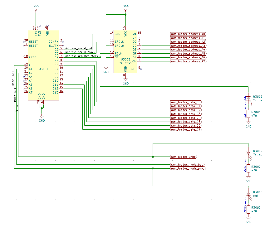
Once the binary file is obtained, it was required to load the code into the memory. For this I used an Arduino nano connected to a 74HC595 in a way very close to Ben Eater's EEPROM programmer.
The Arduino will take over the Address and Data bus of the memory by activating the PROG mode, this basically disconects the memory from the Bus through 75HCT245 chips. Once the memory is isolated, the arduino will go through all the needed address using the 75HC595 (a shift register) and upload the data.
Note :
- a dedicated signal is used to write the value on the bus to memory
- Lines A0 to A2 of the arduino are set to digital
- Yes it would be possible to connect directly all 8 lines of Data and 8 lines of Address to the arduino but I wanted to try out the shift register for the time I will have more lines.
Overall everything works and it a good way to finish 2019. I hope 2020 will bring new features such as:
- PCB backplane with a 5A power supply
- Stack Pointer register with associated Push and Pop
- new ALU with compare, logic operations, etc
![]()
-
It's alive
12/17/2019 at 11:06 • 0 commentsHappy to say that the Nits CPU is now alive and Turing complete. The instruction set is quite small but it runs at both slow (300 Hz) and fast (1 Mhz) speed.
The instruction set includes:- NOP : do nothing
- HALT : halt the computer, at this stage, only a manual reset can restart it
- ADD : add content of register A and register B and store the result in register A
- SUB : substract the value stored in register B from the value stored in register A and store the result in register A
- OUT A : output the content of register A as a decimal unsigned value on the display
- OUT B : output the content of register B as a decimal unsigned value on the display
- LD A, B : copy the content of register B in register A
- LD A, x : copy the content of the memory at address x in register A
- LD A, i: copy the value i in register A
- LD B, A : copy the content of register A in register B
- LD B, x : copy the content of the memory at address x in register B
- LD B, i: copy the value i in register B
- LD x, A : copy the content of register A at memory address x
- LD x, B : copy the content of register B at memory address x
- JMP x : unconditionnal jump at address x
- JMPC x : jump at address x if carry flag is set
- JMPZ x : jump at address x if zero flag is set
It is now time to improve on it.
 Ced
Ced