* * HARDWARE OVERVIEW * *
The CH552 is a little MCU with a 8051 core and a USB interface, and is damn cheap.
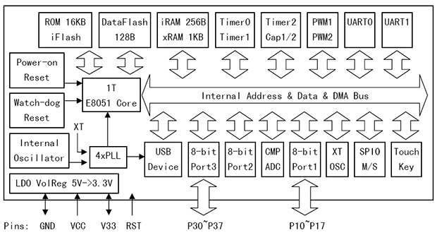
Here are some key data (for more info see this English-ish datasheet):
- 8051 core with most standard registers, commands etc. (8x-15x faster than the original core);
- Integrated oscillator;
- USB 2.0 Full Speed;
- USB-C support;
- 2x UART
- 3x timer;
- 2x 8bit PWM;
- 1x SPI master / slave;
- 4x ADC 8bit input;
- 6x touch input;
- 16KB Flash;
- 1KB xRAM;
- 256B iRAM;
Remember that the 16KB Flash is shared with the bootloader, so the space for the "application code" is a little less (14KB):

So far I have never used an 8051 core, so this seemed like a good opportunity to try it out.
So I bought a small lot of the SO-16 version (CH552G) and made a little board to play with it, the CH552 Dragon... :-)
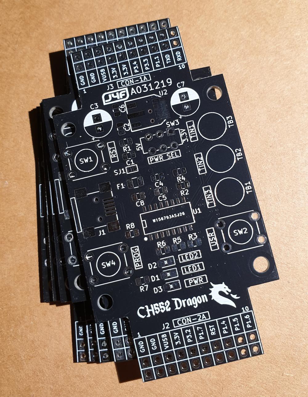
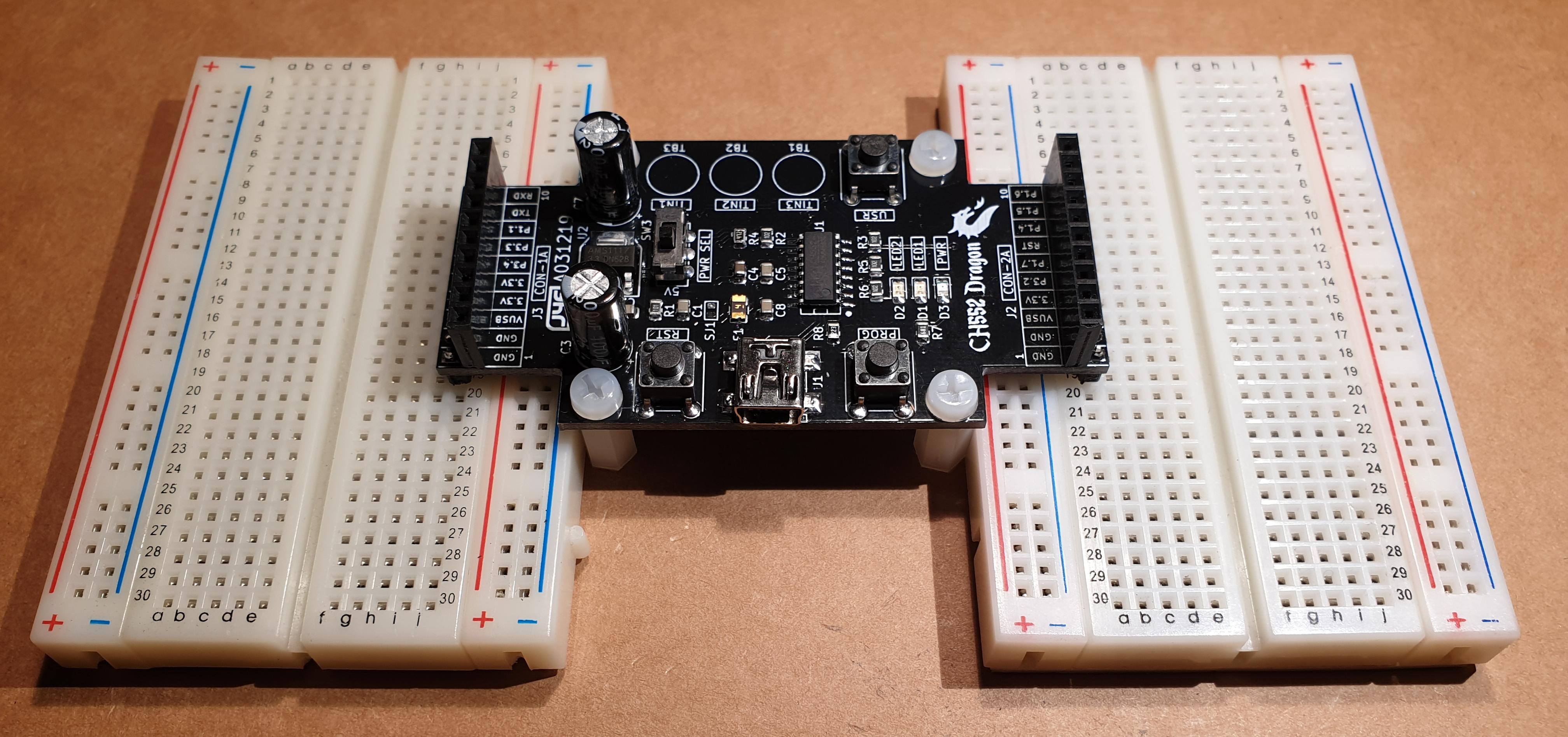
The board follows the same "layout concept" of the previous ARMando, so can be directly inserted in one or two breadboards:

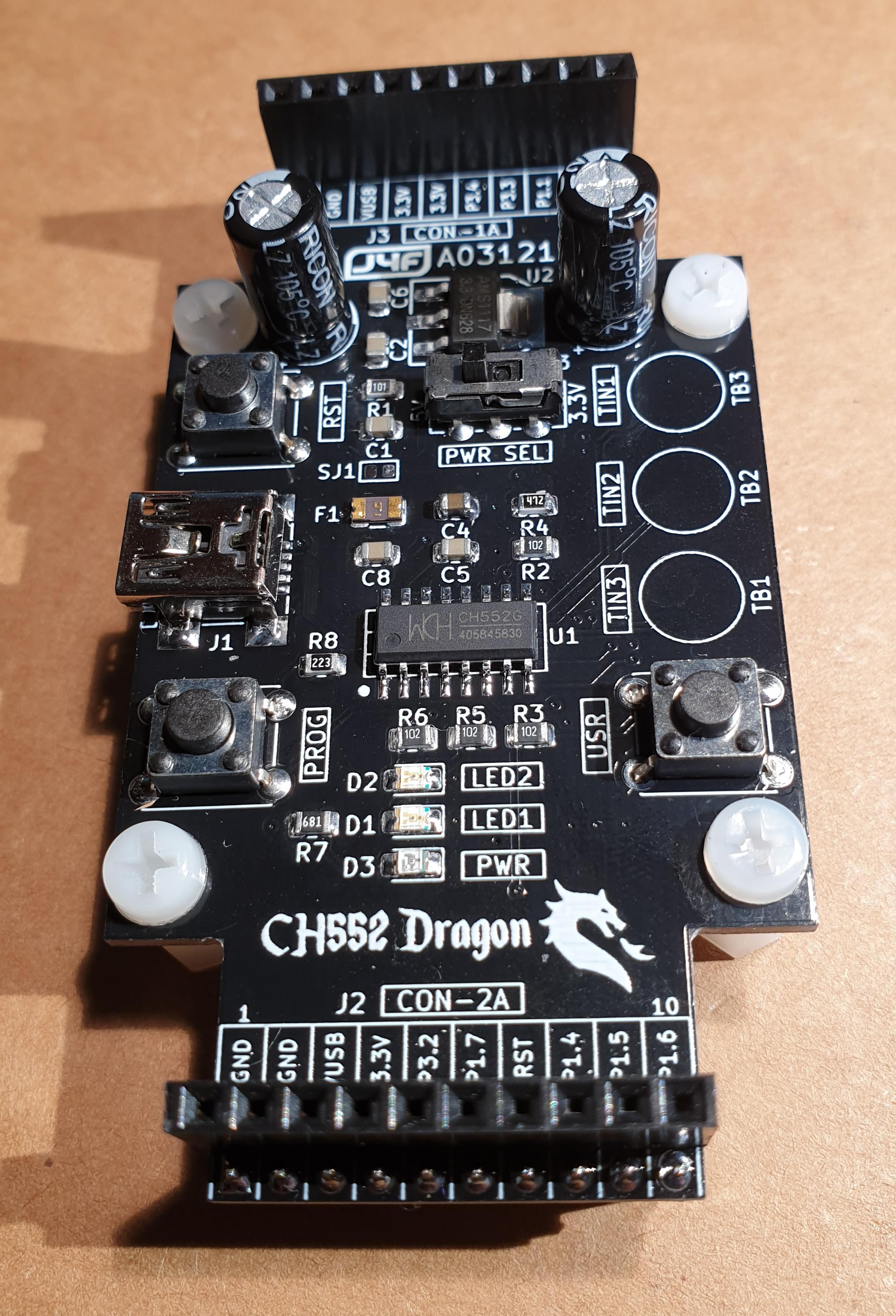
On the CH552 Dragon I've added a physical "user" key (USR) and three touch buttons (TIN1, TIN2 and TIN3) because the CH552 has the hardware to use them.
There is also an optional 3.3V power supply (you can choose not to populate it if not interested, see in the schematic the PWR3 option) to choose the GPIO supply between 5V or 3.3V (i.e. if you want connect it to 3.3V stuff) using the PWR SEL switch.
All the official documentation of the manufacturer (WCH) is written only in Chinese, but using Google Translator can be more readable for sure. Here a link to the CH552 product page with automatic English translation.
* SJ1 AND THE PWR3 OPTION *
The CH552 can work at 3.3V, so I added an optional 3.3V regulator (see at the schematic the PWR3 option). The selection between 5V and 3.3V is made with the PWR SEL switch. Make the selection when the board is not powered.
When the 3.3V is selected, all the GPIO pins work at 3.3V logic levels.
Remember that the CH552 ca be programmed only if powered at 5V, so the PWR SEL switch must be at 5V to enable flash writing.
If you are not interested to the 3.3V power source, the PWR3 option can be left unpopulated on the PCB. In this case leave SW3, C6, C7, R4, U2 unpopulated and close the SJ1 jumper as in the following image:

WARNING: close the SJ1 jumper * only * if the PWR3 option is not populated!
* SJ2 AND SJ3 JUMPERS *
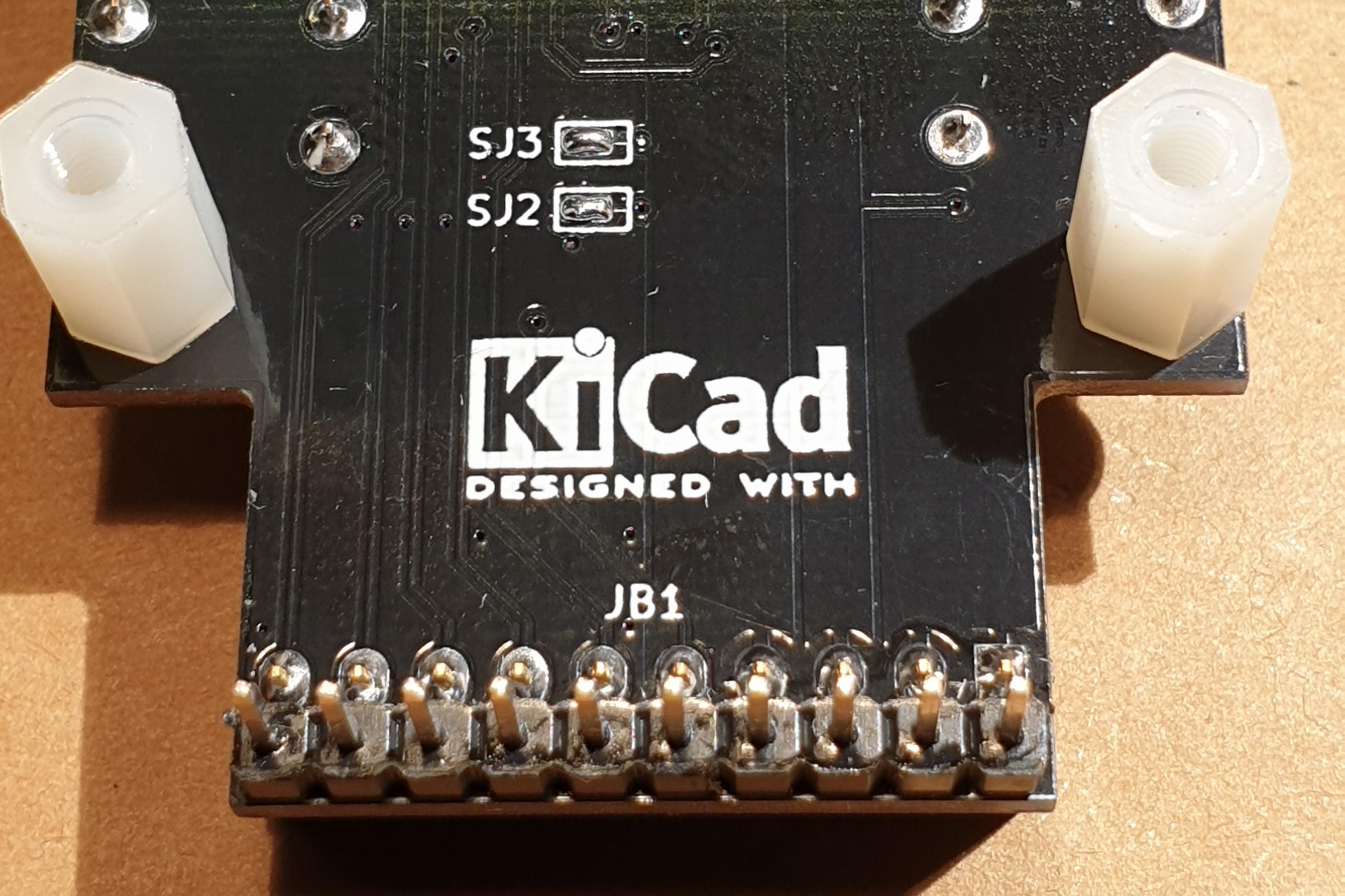
Please note that both the LED1 and LED2 led have a dedicated solder jumper in the bottom side of the PCB. If you want enable them you have to close both the SJ2 and SJ3 jumpers:
* * SOFTWARE OVERVIEW * *
To program the CH55X MCU family it is available an open source C toolchain based on the SDCC compiler and can be found on Github (there are also some examples, but not all of them seem to work).
In the same repository there is an english translation on the CH554 manual (the MCU version that adds the USB Host capability) and can be used for the CH552 too.
In the following video there is the usual blink test example:
To flash the executable .HEX file I've used here (on Windows 10) the original tool made by WCH (WCHISPTOOL) that can be found here.
The CH55X MCU comes with a bootloader that allows to use both the USB (used in the previous video) or the serial interface (the bootloader "eats" 2KB of the flash space, and cannot be overwritten using the USB or serial interface).
To program the CH552 you need a 5V supply (the CH552 can work at 3.3V too but you can't program it): press the PROG button and then power it (i.e. attaching to an USB port).
The PWR SEL switch, if populated, must be in the 5V position to allow the MCU programming.
It is not possible to activate the bootloader pressing the RST and the PROG key, but a power-on is needed (with the PROG key pressed). You can avoid this annoying detail if you add in your source code the option to jump to the bootloader (i.e. pressing a key).
Remember also that accordingly with the datasheet the program flash has a "guaranteed" number of 200 write cycles.
 Just4Fun


 greg
greg
 Ken Yap
IIRC, the CH552 does not need to be powered at 5V to do flash programming. What is needed is that the 5V pin is powered. Long story short: see schematic. Running at 16MHz, GPIO's at 3.3V. https://oshwlab.com/koendv/si5351-clock