-
Another strange idea after a long break...
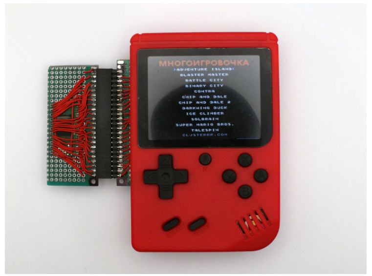
03/23/2024 at 15:16 • 0 commentsOn and off, I had been experimenting on this but with very little success.
There are too many unknowns and trying to guess how it works by modifying the code and reprogramming the flash could be too time consuming.
Later, I came up with the strange idea of connecting the vacant flash pins on the board to another microcontroller and have this microcontroller pretend it is some form of flash.
How I did that:
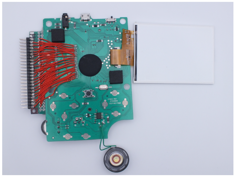
- Soldered the vacant flash pins with 1.27mm pitch ribbon cables (22 pins each),
- Taped the soldered wires with the Kapton. The lines on the PCB are very, very flimsy and could not tolerate a lot of movement at the solder points!
- and connect two female IDC sockets (more than 22-pins) on the other end of the wire (not shown here):
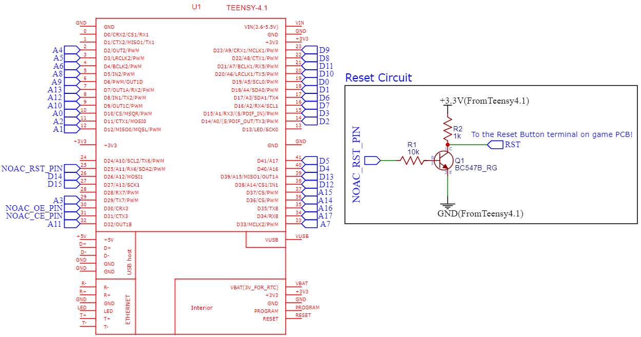
Oh, and a lot of jumper wires to connect this back to the Teensy 4.1 from the end of the female IDC connector . Here is the rough schematic (also note the white cable connected on the Reset Pin which is the "RST"):
It should be something like this in the end (pardon the mess! I will draw another cleaner diagram for this one!):
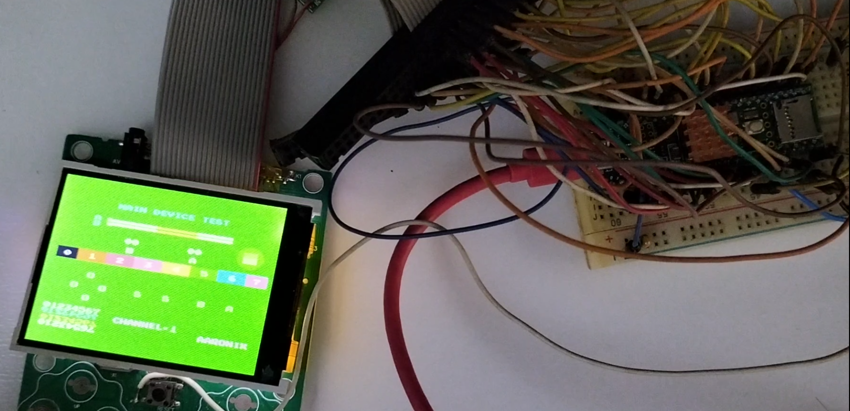
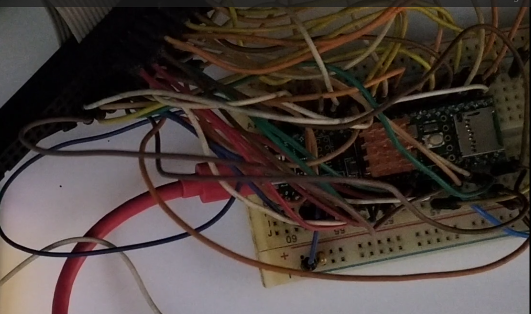
Well, all the pins are connected. Looks frustrating, and I got it done after a few weekends on this!
What would ever happen if I program the Teensy to manually feed the whole game board some instructions?
-
New Git found: "SUP Console Programmator"
02/23/2023 at 15:37 • 0 commentsWhen trying to find ways and means to put our custom compilation inside the flash, I bumped into this very recent article (it is in Russian - you need a Google Translate) explaining about the dumping and the flashing process of the chip inside.
Also, the author documented the rest of the process in the Github (it is in Russian too - Google Translate works on it) - it is an extremely good read.
The method would help me to dump and flash the ROM faster, and also to help me understand that program inside better.
From the article, the pictures are the attempts to build a makeshift "cartridge" that holds that flash board and the "slot" connected to the SUP console:
(Source: Thanks to Aleksandr Serdyukov - https://habr.com/ru/post/718366/)
On that, I will try to build this too and experiment it! :)
-
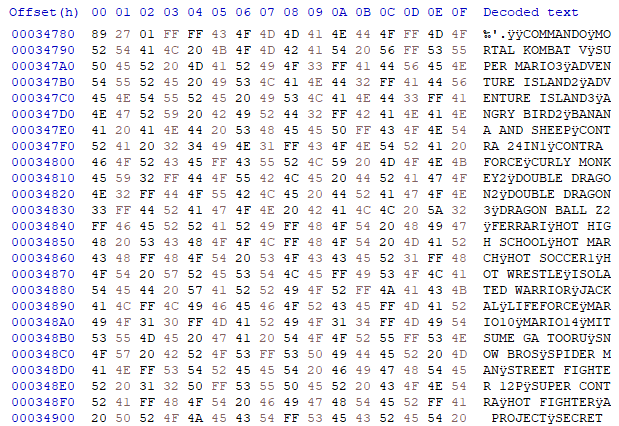
Dump complete! Disassembling the Menu in progress...
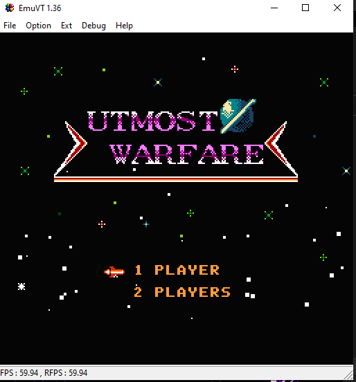
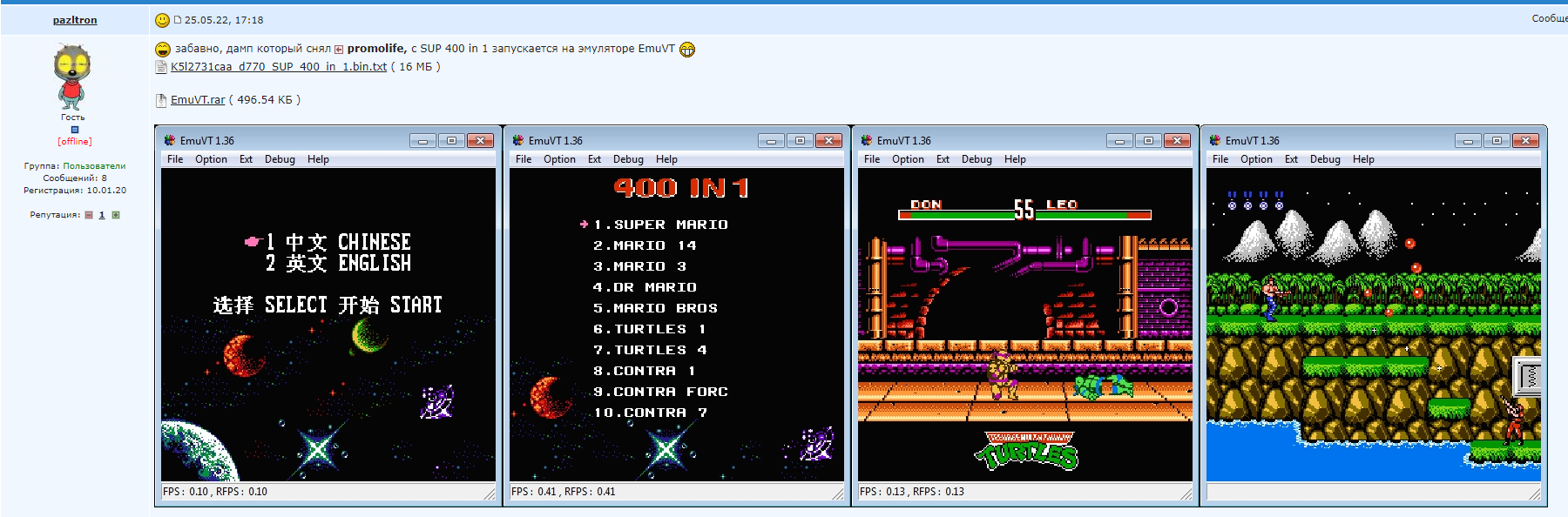
02/23/2023 at 15:25 • 0 commentsFinally, after the one whole day it dumped the contents, I immediately used the BIN file to test it in the EmuVT 1.36. (The latest version doesn't work properly, the screen blacked out when scrolling the menu)
It just worked! Some of the games doesn't work - it could be the dumping issue, or the emulator issue. However, most of the game worked flawlessly:
(What is Utmost Warfare??? And that music... Urgh!)
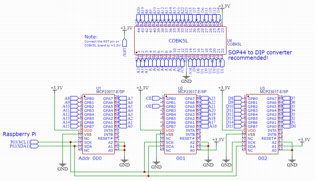
Due to many, many reasons, I felt uncomfortable putting this ROM image here - since the method of dumping is possibly correct, you can replicate this process using the Raspberry Pi, a bunch of wires, and 3 MCP23017s. Here's a rough schematic:
Here is the Python code - I accidentally did a dump from 0x800000 to 0xFFFFFF, but the contents are mirrored from 0x000000 to 0x7FFFFF so the dump still worked as usual! Use a Raspberry Pi according to the schematic too.
Caution: The Python code is quite messy - it has not been finalized. This dumping process takes almost a whole day!
import time
from datetime import datetime

import board
import busio
import digitalio

from adafruit_mcp230xx.mcp23017 import MCP23017

# ROM dump utility
print("ROM dump utility")

# Initialize the I2C bus:
i2c = busio.I2C(board.SCL, board.SDA)

mcp00 = MCP23017(i2c, address=0x20)
mcp01 = MCP23017(i2c, address=0x21)
mcp02 = MCP23017(i2c, address=0x22)
# mcp00 = addr (A0-A15) [A+B]
# mcp01 = addr (A16-A23) [A]; /CE, /WE, /OE [B]
# mcp02 = data (D0-D15) [A+B]

# setting data pins:
mcp02.iodira = 0xff
mcp02.iodirb = 0xff
mcp02.gppua = 0x00
mcp02.gppub = 0x00

# setting address pins (A0-A15):
mcp00.iodira = 0x00
mcp00.iodirb = 0x00
mcp00.gpioa = 0x00
mcp00.gpiob = 0x00
mcp00.gppua = 0x00
mcp00.gppub = 0x00

# setting address pins (A16-A23):
mcp01.iodira = 0x00
mcp01.gpioa = 0x00
mcp01.gppua = 0x00

# setting control pins (/CE, /WE, /OE):
# bit 0 = /CE
# bit 1 = /WE
# bit 2 = /OE
mcp01.iodirb = 0x00
mcp01.gpiob = 0x07
pinCE = mcp01.get_pin(8)
pinWE = mcp01.get_pin(9)
pinOE = mcp01.get_pin(10)

pinCE.switch_to_output(value=True)
pinWE.switch_to_output(value=True)
pinOE.switch_to_output(value=True)

pinCE.pull = digitalio.Pull.UP
pinWE.pull = digitalio.Pull.UP
pinOE.pull = digitalio.Pull.UP

pinCE.value = True
pinWE.value = True
pinOE.value = True

def _CE(en):
    if (en == True):
        pinCE.value = False
    elif (en == False):
        pinCE.value = True
    else:
        raise Exception("True or False only!")

def _OE(en):
    if (en == True):
        pinOE.value = False
    elif (en == False):
        pinOE.value = True
    else:
        raise Exception("True or False only!")

def putAddr(addr):
    mcp00.gpioa = (addr & 0x000000ff)
    mcp00.gpiob = (addr & 0x0000ff00) >> 8
    mcp01.gpioa = (addr & 0x00ff0000) >> 16
    #print("mcp00 gpioa = " + hex(mcp00.gpioa))
    #print("mcp00 gpiob = " + hex(mcp00.gpiob))
    #print("mcp01 gpioa = " + hex(mcp01.gpioa))

def getData():
    dataL = mcp02.gpioa
    dataH = mcp02.gpiob
    return (dataH << 8) | dataL

def readAddr(addr):
    value = None
    putAddr(addr)
    _CE(True)
    #time.sleep(0.01)
    _OE(True)
    #time.sleep(0.01)
    value = getData()
    _CE(False)
    _OE(False)
    return value

def dumpROM():
    for addr in range(0x800000, 0xffffff,1):
        print("Reading block: ", hex(addr))
        f.write(readAddr(addr).to_bytes(2, byteorder="little"))

f = open("romdump.hex","wb")
f.seek(0)

# possibly read only 8 megabits!
#f.write(readAddr(0).to_bytes(2, byteorder="big"))

startTime = datetime.now()
addr = 0
#524288
#f.write(readAddr(addr).to_bytes(2, byteorder="big"))
# let's read each 2048 blocks first!
dumpROM()
stopTime = datetime.now()

print("time taken: ", stopTime-startTime)
f.close()
What's next? I'm trying to understand how the menu and the Aaronix Test screen works. I suspect this had to do a initial startup on the LCD and possibly some other peripherals.
-
Attempt no.2 : New information!
01/25/2023 at 12:52 • 0 commentsYes, it has been a very long time since I updated here due to the lack of information on these little things.
Previously, I have only managed to get a partial dump of the ROM - possibly only the first 8 megabytes.
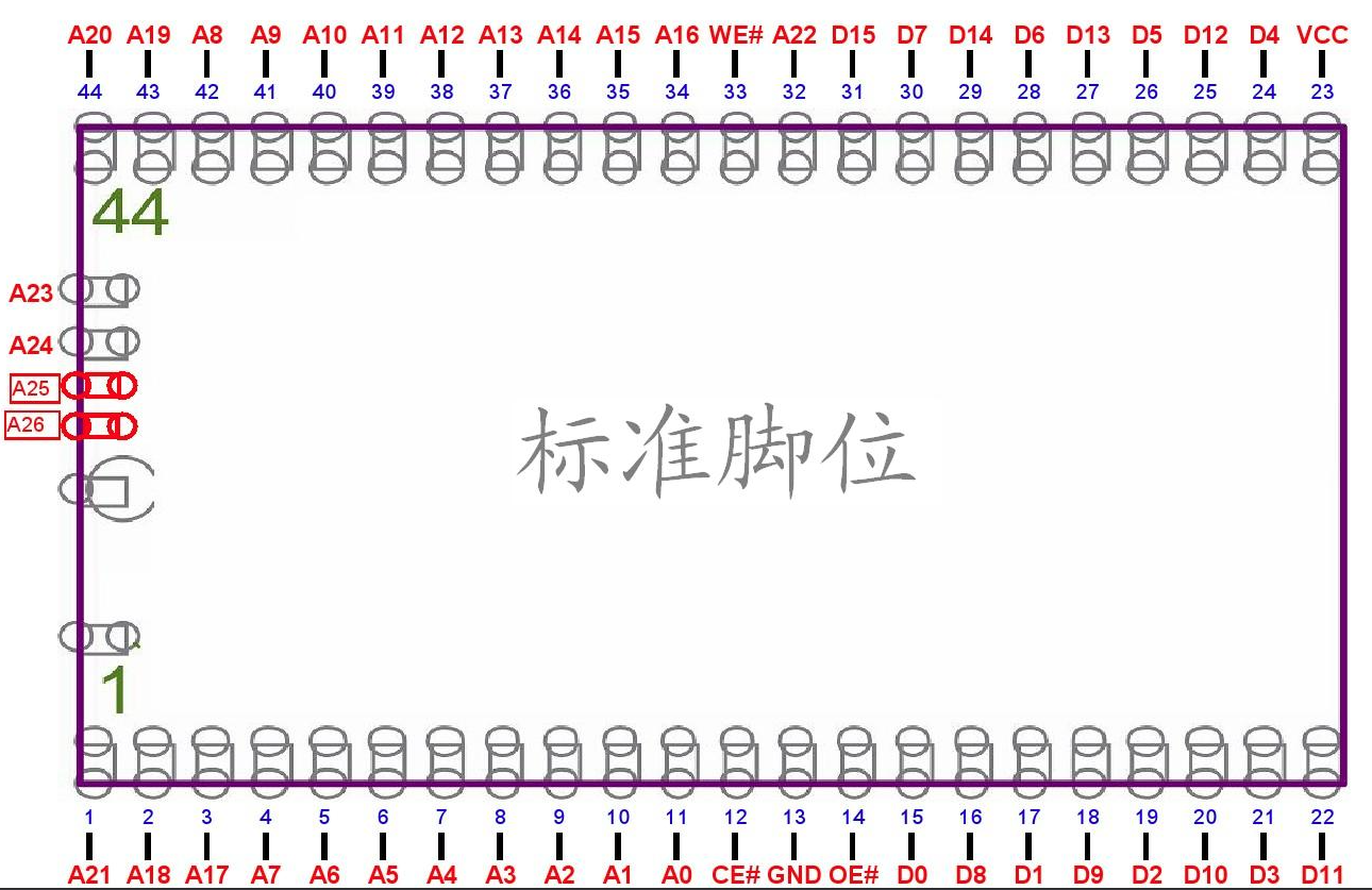
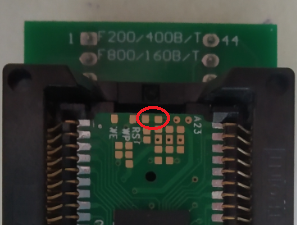
However, someone on the 'net has managed to upload another schematic of the ROM carrier board - this time there's a slight variation on the A22 and A23 pin which I couldn't locate earlier:
![]()
(Thanks to the person who uploaded this - I couldn't find this link anymore!)
I took out that dumper board which I made it using the Raspberry Pi and some MCP23017s since 2020 and tried to reconnect the A22 and A23. However, the dumping is pretty slow and could take a day or so, and as a little preview I managed to see some menu cut-outs and game titles inside (I dumped from 0x80000 onwards). I believe that it has a menu in Mandarin too:
And I found a list of game using the HxD too:
Earlier in 2022, someone examined the ROM dump and uploaded it into a forum, however these dumps couldn't be downloaded, it's a broken link instead: https://4pda.to/forum/index.php?showtopic=979648&st=480:
Not only the person had dumped it but he/she had possibly get it to work using the EmuVT emulator:
Also, there are a number of videos that is showing the unit being modified to play other compilation of games:
There are no schematics provided or instructions posted in these videos, so if there are any new information on these, you can put in the comments below! :D
-
What a big dump! Analysis no. 1!
11/29/2020 at 06:14 • 0 commentsPardon me for that title. The dump means I dumped that 8 Megabytes worth of contents from that ROM I described earlier.
After a few more hours of dumping through Raspberry Pi and extracted its BIN file, I noticed that:- Suspected inconsistent addressing beyond 64KB
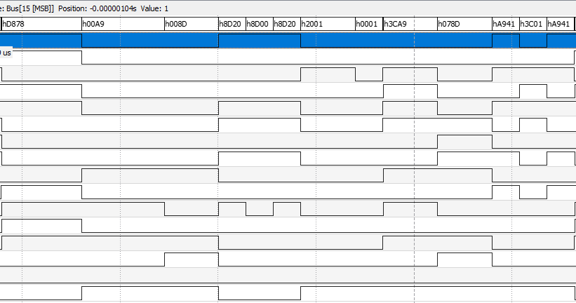
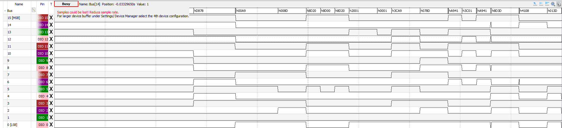
- I peeked into the original snapshot of the bootup from the bus analyzer from Analog Discovery 2:
Then, in the same fashion, I sniffed out the last 8-bit of the address from the bus analyzer:
The top 8-bit address during the bootup shows a 0x02 and 0x03 - but I couldn't find that exact bootup code from above with that higher address in the BIN file. That leads to...
- I peeked into the original snapshot of the bootup from the bus analyzer from Analog Discovery 2:
- Incomplete memory dump
- This BIN sample has been analyzed by an experienced member in BGC forum: http://bootleg.games/BGC_Forum/index.php?topic=2884.0
- It is incomplete - I looked high and low for the menu cut-outs and hints of it but couldn't see them.
- Highly suspected that the last address A24 isn't accessible - it ends up mirroring whatever contents from the first 8MB.
I have another sample of this and planning to extract and see if these are the same thing or not.
- Suspected inconsistent addressing beyond 64KB
-
Dumping - first try!
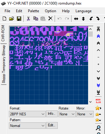
11/14/2020 at 15:16 • 0 commentsAfter messing with the Python script, I started to dump the whole thing. As a first try, I did dump a few kilobytes of data. Using that YY-CHR app (https://w.atwiki.jp/yychr/), I'm seeing something - there are sprites, cut-outs and whatever that looks very familiar. However, they look pretty distorted and this one looks like letters and numbers in 8x8 fonts but they look mashed up pretty badly:
After changing how it dumps the code (the endian-ness) I can see something more clear here now:
As this code is not really polished and experimental, I'll be putting up the code and schematics on Github once I get the proper full dump. Next thing is, try to dump the entire thing and possibly run it with the modified Nintendulator which works on the VT-03 ones.
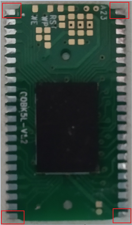
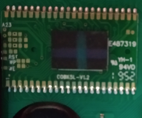
Good thing is at least the ROM carrier board is based on the one that is shown earlier (link: https://www.eevblog.com/forum/beginners/fun-project-hack-cheap-handheld-console-help-with-bga-nand-flash-chip-needed/):
-
Extracting the ROM board and attempt dump!
11/14/2020 at 15:03 • 0 commentsAfter getting the ChipQuik and try to manually remove the thing without overheating it (I hope so), I got the thing out finally!
And with that SO-44 to DIP adapter I have, this will be handy in dumping the ROM without resoldering the wires to the ROM board again.
However, I have to file off the edges a bit just for the board to fit into the adapter:
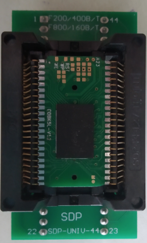
This is how it looks like after it is fitted into the adapter:
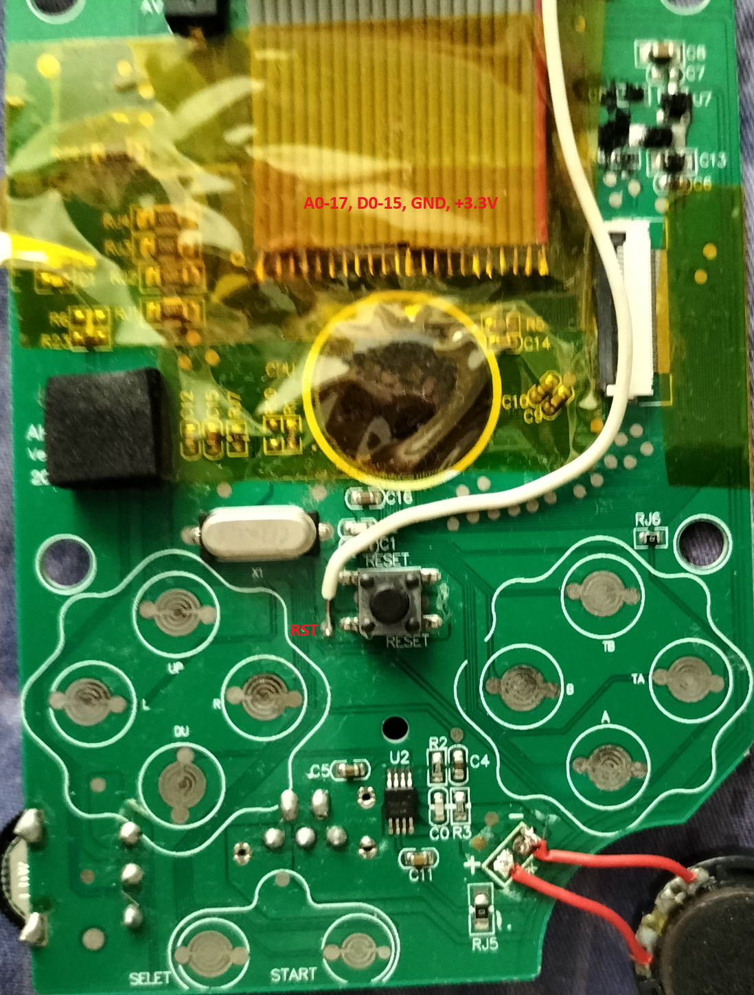
And after connecting it again to the board with MCP23017 and a Raspberry Pi I tried reading the first few bytes just to see a 0xFFFF or 0xFF00 as the data output. It can't be even right and these values are not even consistent! So after a few hours of research and digging, I'm suspecting that there's an RST pin which I missed out:
There it is. After soldering it to +3.3V and reattempted the read, it finally give a meaningful output (or at least it doesn't jump around or keep showing 0xFFFF for multiple reads on the same address).
Next is how am I gonna dump the rest of the whole thing? This is the question and I'm writing up a Python script inside now.
-
On site dump - no dice!
11/01/2020 at 03:06 • 0 commentsI tried soldering the onboard ROM with wires, and extend them to a board with MCP23017s. From that, these are connected to Raspberry Pi and does the job of getting the stuff out while the reset button is hold.
Unfortunately it doesn't work that way. I kept getting random values! The system possibly doesn't hold the address and data high-z during reset.
I have to remove the carrier board out. I would do a hot air, but I'm very unsure if high temperature could kill the contents inside, or it could kill the neighboring NOAC too. May have to resort to another stunt - low melt solder...
Suggestions are welcome here if anyone knows how to remove such a thing (check earlier logs on that carrier board).
-
Is it a boot code? A guess here.
10/25/2020 at 13:03 • 0 commentsFrom the last week's check on the data bus, it looks like there's some resemblance to whatever other dump that comes from this website:
https://forums.bannister.org/ubbthreads.php?ubb=printthread&Board=1&main=7205&type=thread
One of the posts mentioned about a dump from another cheap NOAC console:
E000   D8         CLD
E001   78         SEI
E002   A2 FF      LDX #$FF
E004   9A         TXS
E005   A9 00      LDA #$00
E007   8D 00 20   STA $2000
E00A   8D 01 20   STA $2001
E00D   A2 02      LDX #$02
E00F   AD 02 20   LDA $2002
And here, from the recording of the data bus earlier:
78
D8
A9 00
8D 00 20
8D 01 20
...
It could be a startup code, and this varies on ROM to another ROM. I'm not familiar with 6502's assembler - I might need to try to have the cheat sheet (6502 instruction set list) ready on my side and read it.
I'm now trying to dump the entire ROM and try to dissect it further. It is not gonna be easy, I admit!
-
Reading the data bus - Attempt
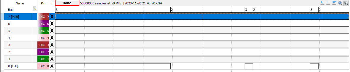
10/17/2020 at 11:59 • 0 commentsI'll start with the data bus since it's 16-bit wide and this is the maximum number of lines that the Analog Discover 2 can handle.
As usual, here's what it is shown during the bootup:
There are a few issues there:
- Not sure whether the ROM pinout is the one that is shown in the earlier log. There are risks of reading the wrong bit or reading the wrong address lines. However, from that website http://www.retrobits.es/2015/08/28/dduc-tuneando-la-mierdaconsola-8bit-que-regalo-abc/, it seems that this ROM pinout is actually compatible to the ST's M59PW1282.
- No CLK line that can be extended for my use on this one. Sadly, the only CLK line is on the 21.47MHz crystal on that board. It can get difficult to see which instruction is actually executed.
- Measuring between the values shown on the bus provided gives timings that are multiples of 1.79MHz CLK periods (approx 558.66nS). Highly suspecting that the CPU is really running on 1.79MHz.
- On a check of a basic 6502 system - the data bus is 8-bit. It is not known how this particular 6502 (or derivative??) can have a 16-bit bus. These clones of NES are very well known to have retrofitted 6502s with extra peripherals. Here, the difficulties of understanding the system increases because it is not understood how it fetches the instructions. Is it most significant byte first? Or the least?
In the meantime I'm going to look into these instructions that are sniffed out and see if they actually make sense or not.
Dissecting a hand-held NOAC console (Sup 400-in-1)
This is an attempt to understand how these little things work, and what we can do on it.
 (Source: Thanks to Aleksandr Serdyukov -