Close
0%
0%

Applix 1616 Documentation

OCRd and typeset as html where possible. A work in progress.

Similar projects worth following
An interesting 68000 machine, using just TTL and two PAL16R8 chips to produce 2-bit and 4-bit colour video. I collected all the scanned articles I could find, and OCR'd as much as I could to get them into a more readable form.

I'm aware of many issues with my collection. I've been informed that not every is attributable to ETI, for example the Forth manual was written by Eric Lindsay directly for Applix. I should probably file the lot under the com/Applix directory, and say which ones were published in ETI.

Note that I am not here to pass off other people's work as my own, but merely to OCR and re-typeset material in html format, freeing them from obsolete Desktop Publishing software. 

I only made a start on the Forth manual, because it is not a very popular language and does not merit spending much time on it. It is not top-priority hobby work because 1616 enthusiasts are a minority.

I can't actually host the html on hackaday so I'm more than happy for the copyright owners to do so.

I was buried in paid work until recently, but am happy to comply with copyright holders' wishes.

Recreating the PAL devices is my main concern, as they are the only obstacle to recreating the 1616 completely. I have the timing diagrams of an Atari machine, which is a good starting point. Without any information or access to the 1616 chips or waveforms, it is impractical to try cloning them. However, I thought it might be possible to make a primitive 1616 circuit that is just a 68000 (or 68008) chip that runs a loop generating video access DRAM cycles. I have some spare CPUs in my collection. Alternatively I could try creating a model in FPGA.

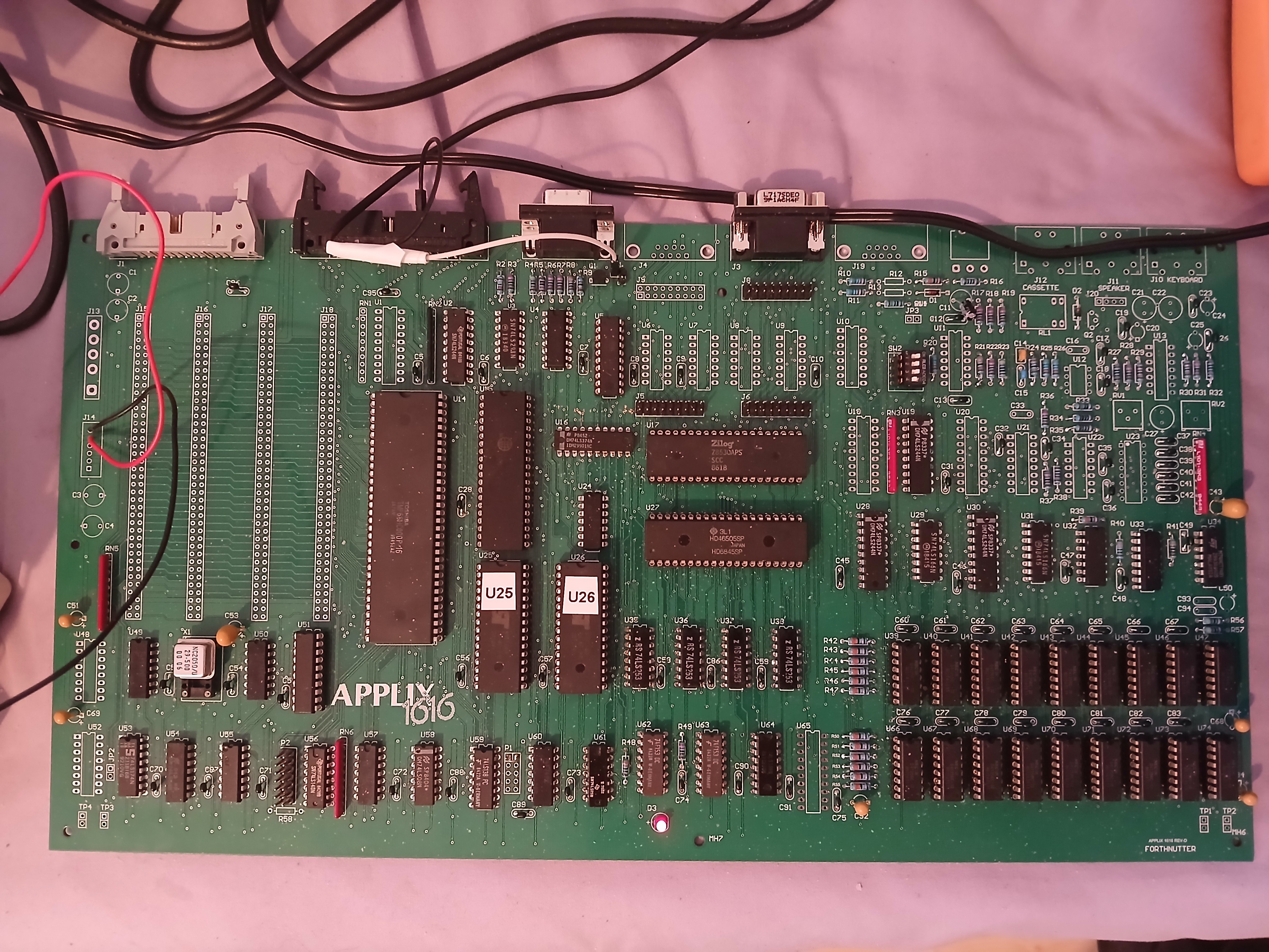
Recently I was kindly sent a 1616 PCB remake designed by Forthnutter. So I bought the bits to make it up as the ultimate testbed - the real thing.

Most recently I was sent a pair of original PAL chips, and found the security bits had not been blown so they were readable! That avoided a lot of hard work guessing the fusemaps from the behaviour.

There are now three 1616 boards under construction.
1616test.s.txt

Rough test code patch for ROM. A work in progress. Uses no RAM.

plain - 6.66 kB - 08/10/2026 at 19:56

Download

Bellcore MGR Window Manager.html.zip

The pdf file converted into an html file.

Zip Archive - 59.22 kB - 06/19/2026 at 19:24

Download

Applix-1616-Bellcore-Windows-Manager.pdf

Bellcore MGR Window Manager software provides an API to manage windows on a high resolution screen. This requires hardware mods for a 30 MHz pixel clock, and replacing U3 (a 74LS298) with a PAL16L8. And of course a suitable monitor.

Adobe Portable Document Format - 202.41 kB - 06/19/2026 at 14:06

Preview

Applix 1616 programmable logic files.zip

1616U5.JED, 1616U51.JED PAL16R8 chip fusemaps, read by Dataman-48 1616U5.EQN, 1616U51.EQN The JED files above, disassembled 1616U5P.JED 1616U51P.JED Compiled for PAL16R8 1616U5E.EQN, 1616U51E.EQN The disassembled, edited to make human readable. 1616U5E.JED, 1616U51E.JED The above, compiled for PAL16R4 1616U5G.JED, 1616U51G.JED and for GAL16V8 analyse.bat DOS file to generate files check.sh BASH file to compare the PAL16R8 fuse maps are the same (apart from pin names) after my edits.

Zip Archive - 12.38 kB - 06/13/2026 at 17:53

Download

1616_U51.EQN.txt

First compilation after looking at original PAL behaviour. Compiles but not tested yet.

plain - 3.92 kB - 06/10/2026 at 00:58

Download

View all 20 files

  • 1 × 68000 CPU, DIP64, 10MHz or better.
  • 16 × 41256-15 256 x 1-bit DRAM, 150ns
  • 2 × PAL16R8 or GAL16V8B NOT 16V8CQ or 16V8ZP !
  • 1 × 85C30 SCC Serial Communications Controller
  • 1 × 6845 CRT controller

View all 8 components

  • Disabling the bus error timeout

    Keith08/07/2026 at 18:02 0 comments

    I wondered if the bus error circuit was generating spurious errors.

    I guessed that bug-free running software would never access an invalid address, so it ought to be alright to disable bus error detection. So I did.

    I cut the track between U33B pin 5 and U24C pin 10, near to U33B, then tied the track to VCC.

    Power on and ... nothing. Not even CRTC initialisation and screen start up. 

    It looks like the bus error handling is essential to sweep the CPU into executing some valid code.

    But really, I would expect the code to present a sign-on screen before trying to access some expansion boards that may be present or not, and not have exception screens overwrite each other before locking up completely. It doesn't seem to be handling itself gracefully.

    Jo is having more success than me, with a couple of known board errors and fixes. So I think any faults are likely to be component or assembly faults. This will take an unknown amount of time.

  • Electrical review

    Keith08/05/2026 at 00:40 0 comments

    Many people learn electronics as a join-the-dots exercise in textbooks written by academics who teach but seldom make practical products. Power lines are drawn with the same pencil-thin lines as signals, connections have zero resistance, inductance or capacitance, and so on.

    Your CAD system will check you have made all the right connections, but it won't tell you if your thin copper track is going to melt as soon as a power transistor gets switched on. Well, as of 2026, but one day AI will be able to do this.

    I have seen professional products designed by people with no appreciation of real-world current flow. Like the battery charger my employers once paid a lot of cash to a subcontractor to design. Heavy currents, thin wires... it did not blow up but it got hopelessly confused trying to measure currents. But that's another story,

    Back to the board we are looking at...

    Power rails

    The power enters on the left, next to the expansion slots. This makes sense because the expansion board could take a lot of current, but I have none so is is not an issue. Or cause of problems that the board is having.

    A good way of telling which chips are using the most current is to feel which are warm or hot. 

    My NMOS CPU was rated at 8 MHz, and the board timings demanded at 10 MHz (or faster) part. I fitted a 16 MHz CMOS CPU, and that runs stone cold.

    The NMOS SCC ran warm even when idle, so I bought and fitted a CMOS version. 

    The 6845 CRTC is also running warm, but that seems to be running without errors so it doesn't seem to be starved of power.

    DRAM is notorious for needing power, and huge gulps of it every time a row address strobe refreshes the charge on a row of capacitors. They are tiny, but there are many on a row and they need topping up in a fraction of a microsecond. Hence the huge current pulse, and the need for a decoupling capacitor for every DRAM chip.

    Some people say that you really need power and ground planes for serious RAM designs, but these extra layers push up the board price. So board designers have to take more care for two-layer boards. 

    The Applix 1616 has the DRAM chips on the opposite side of the power inlet. So all those row-charging current gulps have to travel through the copper tracks across the board, dipping the rails of everything else on the board. 

    The BBC micro got round this by having power input connections specifically for the DRAM chips. This might be something worth adding to the Applix board.

    Let's take a look at the voltage drops. 

    First I set my PSU to deliver 5.2 volts on the power input of the board, then measure the voltage across the power pins of various chips.

    5.008  Input measured at J13.

    4.812 at CPU, ROM chips (3.76% low.

    4.816 at CRTC

    4.817 at SCC

    4.847 at furthest DRAM chip (the worst case) is 3% drop, which is acceptable.

    4.982 at U49

    4.986 at U5 and U51, the PAL chips

    4.990 at U2, , the IC nearest J13.

    With 5.2 volts at J12, furthest DRAM is 5.035 volts.

    So it looks like the 5V power is okay across the board.

    Termination

    I went to a lecture about the BBC micro, and the speaker said that the BBC failed to run reliably until someone held their fingers on the board tracks. They didn't know why, but they added some resistors to the data bus to simulate the resistance of fingers, and the BBC worked.

    Well I could have told them straight away why it didn't work. When you have wires over a board the size of a BBC micro, they stop being a join-the-dots textbook wire and start behaving like a transmission line with inductance, capacitance and reflection. Fingers or resistors act as terminating loads, absorbing energy that would otherwise be reflected to cause overshoots and undershoots.

    The Applix is about the same area as a BBC micro. But it does not have any bus termination at all!

    Right, that needs sorting out!

    Fortunately I have a known-good termination circuit from the STEbus. I'll start by tying...

    Read more »

  • Fixing the reversed characters

    Keith08/02/2026 at 19:55 0 comments

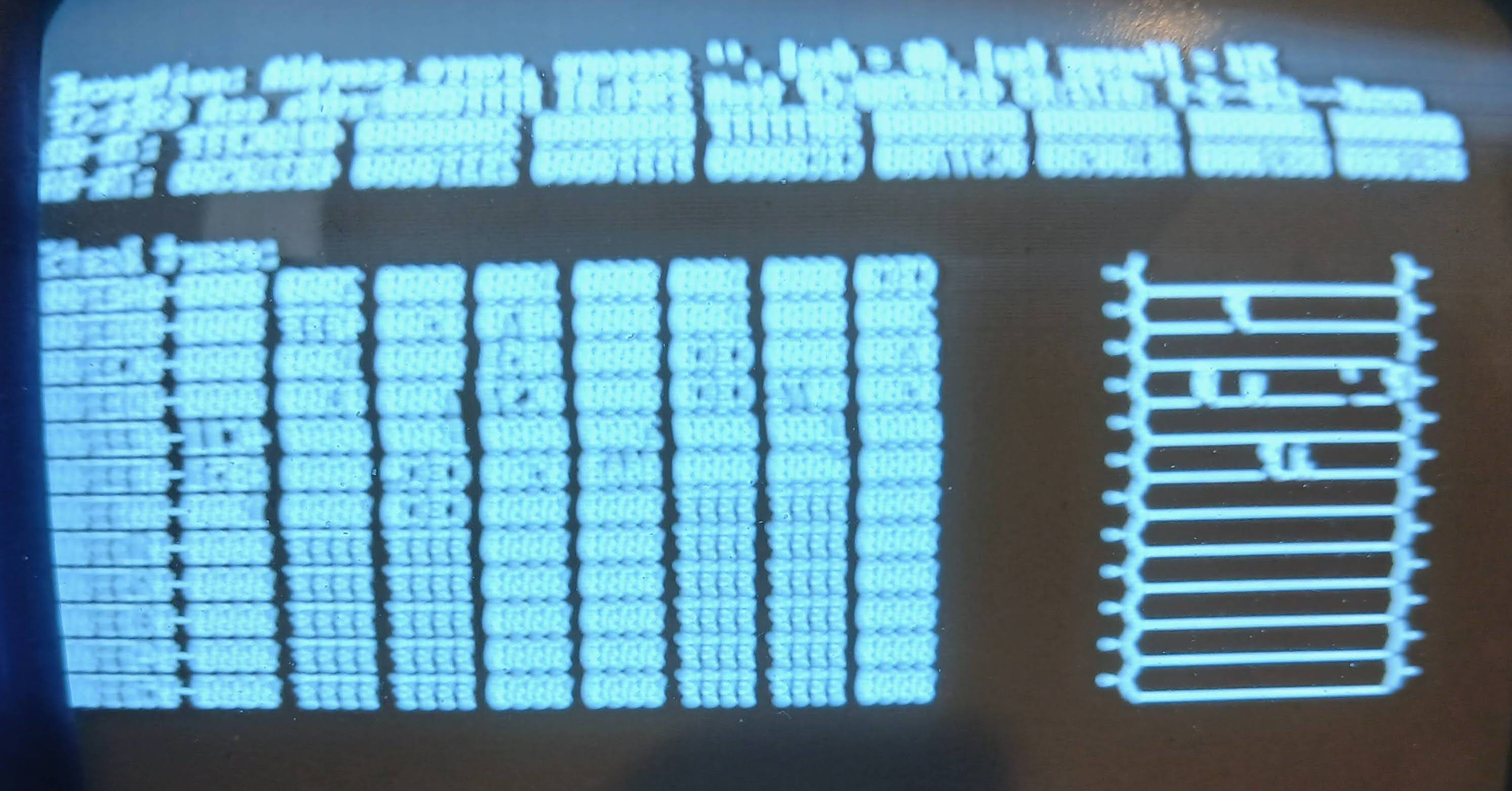
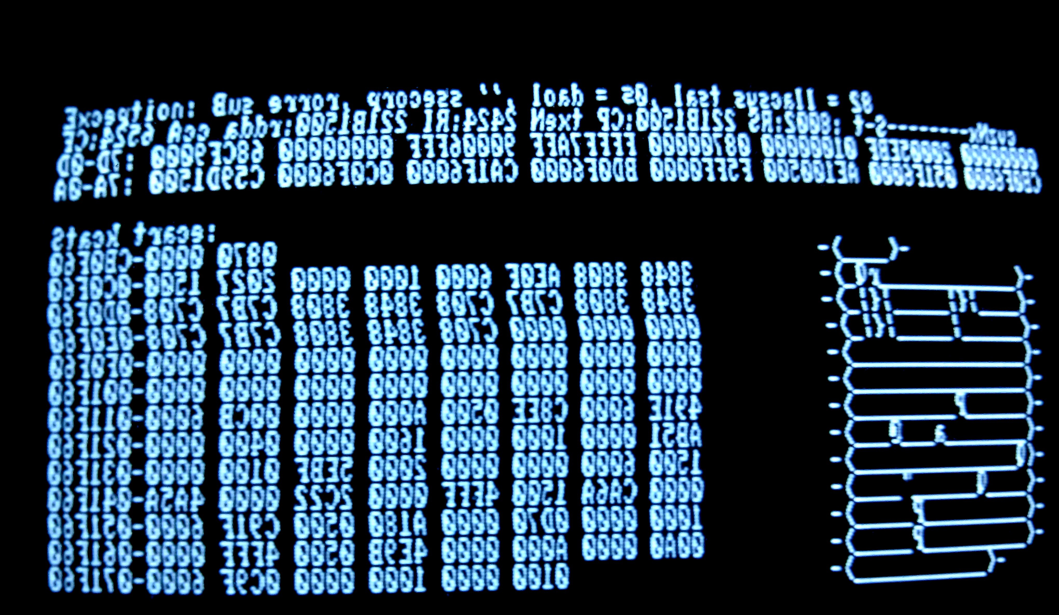
    I managed to reduce the blurring by simply turning the TV brightness down. The text became much more readable. 

    The text translates roughly into this:

    Exception: Bus error, process '', load = $0, last syscall = 28
    FC:4256 Acc addr:0051B122 IR:4242 Next PC:0051B122 SR:2008: t-S--------xNzvc
    D0-D3: 0006FC86 00000000 FFF60009 FFA7FFFF 00000780 00000010 FBE50002 0????????
    A0-A7: 0051D95C 0006F0C0 0006F1AC 0006FODB 0000FF2F 005001EA 0006F150 0006?????
    
    Stack Frame:
    06F0BC-0000 0780
    06F0C0-0051 7202 0000 0001 0006 F0EA 8083 8483
    

    With a stable screen, it looks worthwhile correcting the video shift-register error. 

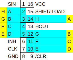
    The shift register sockets look like this:

    Blue are the correct connections on the chip pins, yellow are the wrong positions on the socket holes.

    Therefore, for each LS166 chip:

    • Isolate the blue pins by bending them out of the socket,
      or if they are soldered in then cut the legs off the board but leave pin stumps,
      and remove the pin material from the holes.

    Connect:

    • Hole 2 to pin 14
    • Hole 3 to pin 12
    • Hole 4 to pin 11
    • Hole 5 to pin 10
    • Hole 14 to pin 2
    • Hole 12 to pin 3
    • Hole 11 to pin 4
    • Hole 10 to pin 5

    I didn't manage to isolate the pins neatly, so I removed them, cleaned the holes  and did this.

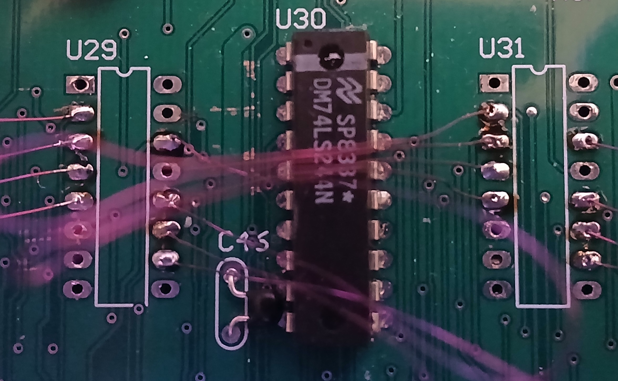
    First add wires to the wrongly positioned signals:

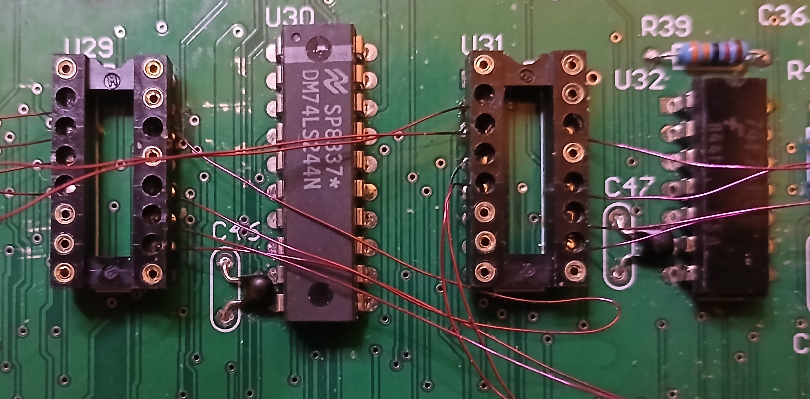
    Then deplete the erroneous pins from some turned-pin sockets, then fit them:

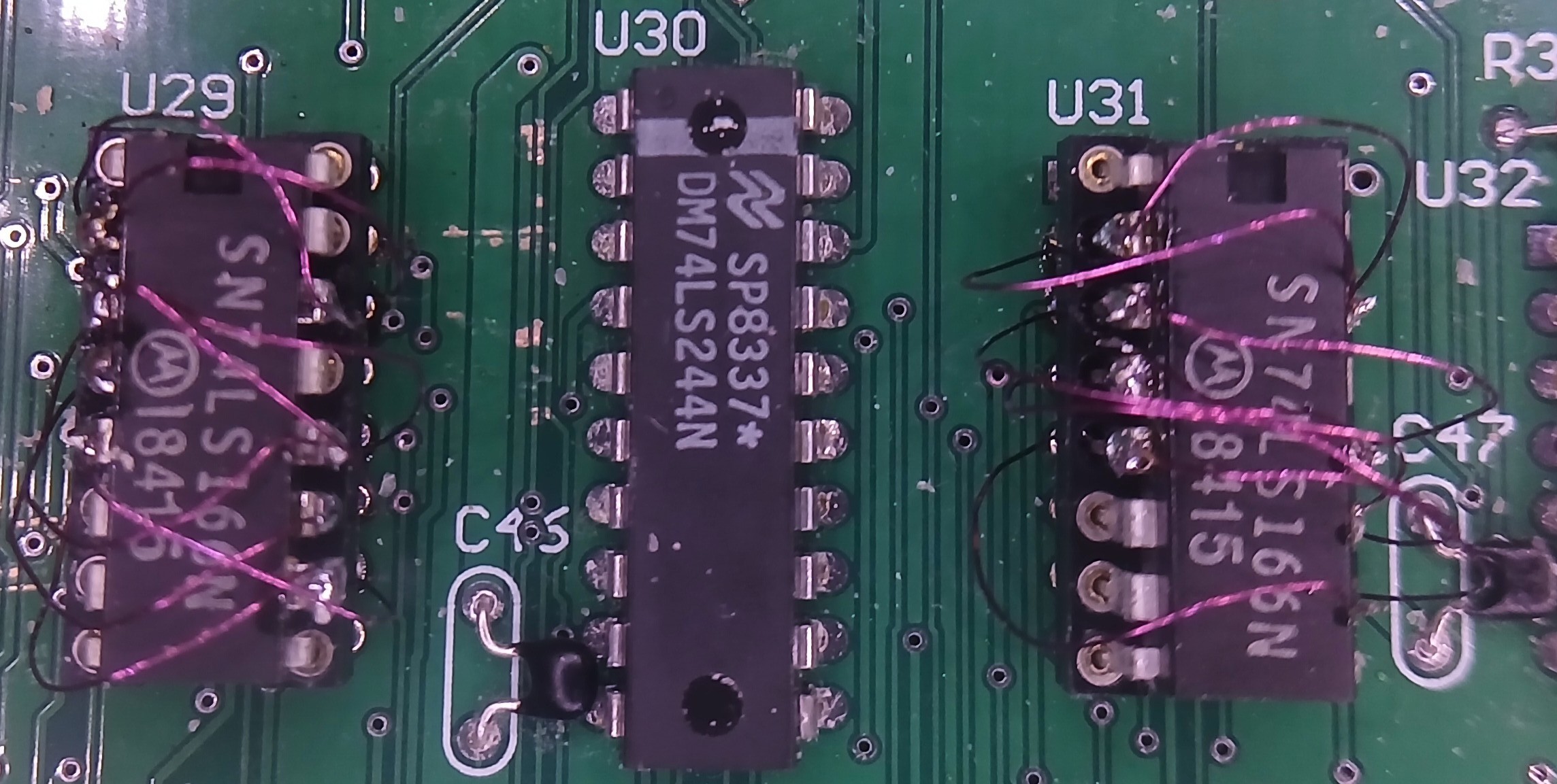
    Then connect the wires to the right pins:

    Yes, it looks messy but it takes less space than forthnutter's correction board.

    With hindsight, it would have been easier to solder wires to the chips first, the poke them through the socket and PCB holes.

    I must have got all the wires right, because I get a sign-on screen with the letters the right way round:

    which immediately does at least two Exception screens before settling. This is a second:

    I get the impression the system is less stable than before, when it would usually just throw one exception.

  • Programmable logic chip investigation

    Keith08/02/2026 at 17:51 0 comments

    I asked forthnutter to send the JEDEC fuse map he compiled with WinCUPL, to compare it with the one I compiled with eqn2jed.

    There was one error in the fuse map defining the green pin behaviour, but not enough to cause the complete lack of pixels on all but the right-hand column of characters.

    There were major differences in the configuration bits. WinCUPL had specified signature bits, while jed2eqn had not specified any. Also, jed2eqn had cleared fuses to ignore unused rows, which saves power. WinCUPL had left them set.

    So apart from current consumption and the minor bit error, forthnutter's GAL should have worked exactly as mine did. 

    Forthnutter is using his original PAL chips and his display is working. I had tried them, without success, but that was before I swapped /CE and /OE drive signals on the Flash ROM chips. So I tried them again.

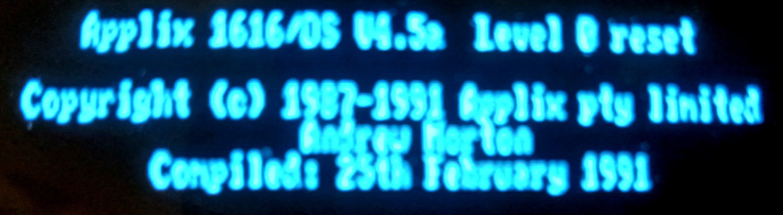
    The behaviour is not stable, but significantly better. It usually briefly displays the sign-on screen, which is very blurred and has individual letters horizontally reversed but should look something like this:

                     Applix 1616/OS V4.5a  Level 0 reset
    
                  Copyright (c) 1987-1991 Applix pty limited
                                 Andrew Morton
                         Compiled: 25th February 1991
                           ROM checksum: $5710FFC2
                        24K RAM disk,  32K video memory
                    0 drivers occupying $0 bytes at $6F1C0
                        System processor: 7.5 MHz 68000
    
    Switch 2 open: ;using SA: for console

    It then jumps to the usual  Motorola 68000 exception crash dump screen.

    Another improvement is that it doesn't keep rebuilding an exception screen over and over again.

    I wondered if there was any differences using GAL chips versus the original PAL chips. It turns out there are.

    The GAL16V8 starts up with outputs high. I had noticed this when comparing the PAL vs GAL behaviours. However, this is the inactive state for most control signals so it is desirable.

    The GAL16V8CZ series are designed for aggressive power saving. They have Input Transition Detection (ITD) circuits that wake the chip very quickly (say 5ns) after any input pin (apart from CLK and /OE) change. This reduces power while inputs are steady. Up to the point where the inputs change so often that the chip never has time to sleep.

    This causes problems for the counter, because if the matrix is waking while the outputs are being fed back, the macrocells can experience setup-and-hold violations relative to the system clock.

    Modern GAL chips are usually much faster, so the fast rising and falling edges can cause ringing and timing problems. So you might be better off with slower speed versions like the 16V8B.

    The power-saving feature can't be disabled on the 16V8, but it can on the 22V10. Which is a good reason for upgrading the 1616 board to use them. It also allows the 15 MHz upgrade logic to fit inside.

    So that is a good step forward. 

    TPAL1 U51 is NS PAL16R8 ANC +B8648 (25 ns)
    VPAL1 U5 is MMI PAL16R8 BCN 8625 (15ns)

    I then bought eight AMD PAL16R8-7 chips. AMD bought up MMI, so they should be the same as MMI chips. At 7 ns, they are a superior replacement for the originals (MMI BCN is ns, NS ANC is 25 ns)

    I programmed a pair, and they did not improve matters. In fact, I can see there are now screen bytes not cleared at start-up. The faster speed may be causing the problem. In fact, that is the only real difference from the original chips, so it must be the problem.

    I have a gut feeling that if faster logic chip causes a problem, then there is something wrong with the overall logic.

    Right now I just want to replace the originals with copies that work just as well, not worse. So I have ordered:

    MMI PAL16R8ACN is 25ns, to replace the NS PAL16R8 ANC (which my LV48 can not program).

    The 15ns versions are a bit scarce/pricey on eBay right now. So I am ordering some GAL16V8B chips of the matching speed.

  • Logic analyser results

    Keith07/30/2026 at 20:53 0 comments

    Two 30 MHz oscillators arrived, and I replaced the 29.5 MHz one I was using. I didn't think it will make much difference, but it did. The 30 MHz oscillator caused the display to keep blinking!
    Maybe it wants more current. Data sheet says 40 mA, about normal for legacy modules.

    I restored the 29.5 MHz oscillator, display is stable. Maybe could do with more decoupling there.

    There are times when a logic probe just won't cut it, and this is one of them.
    Time to get the big guns out, in the shape of my 500MSPS logic analyser.

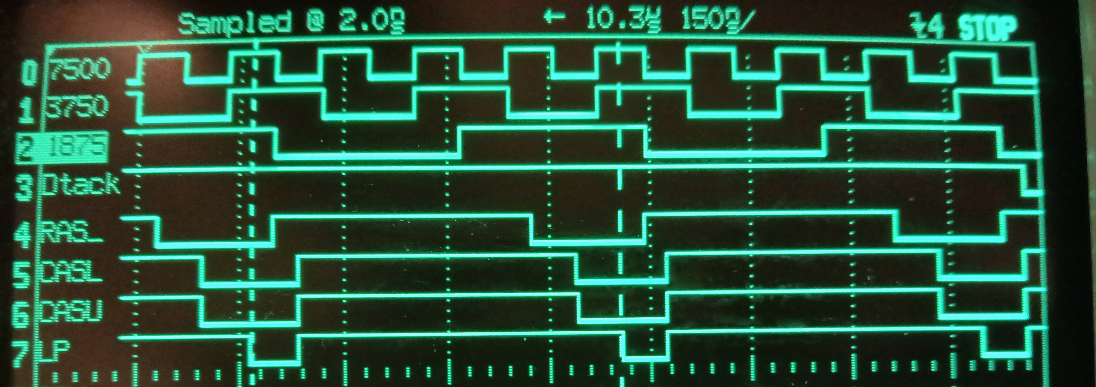
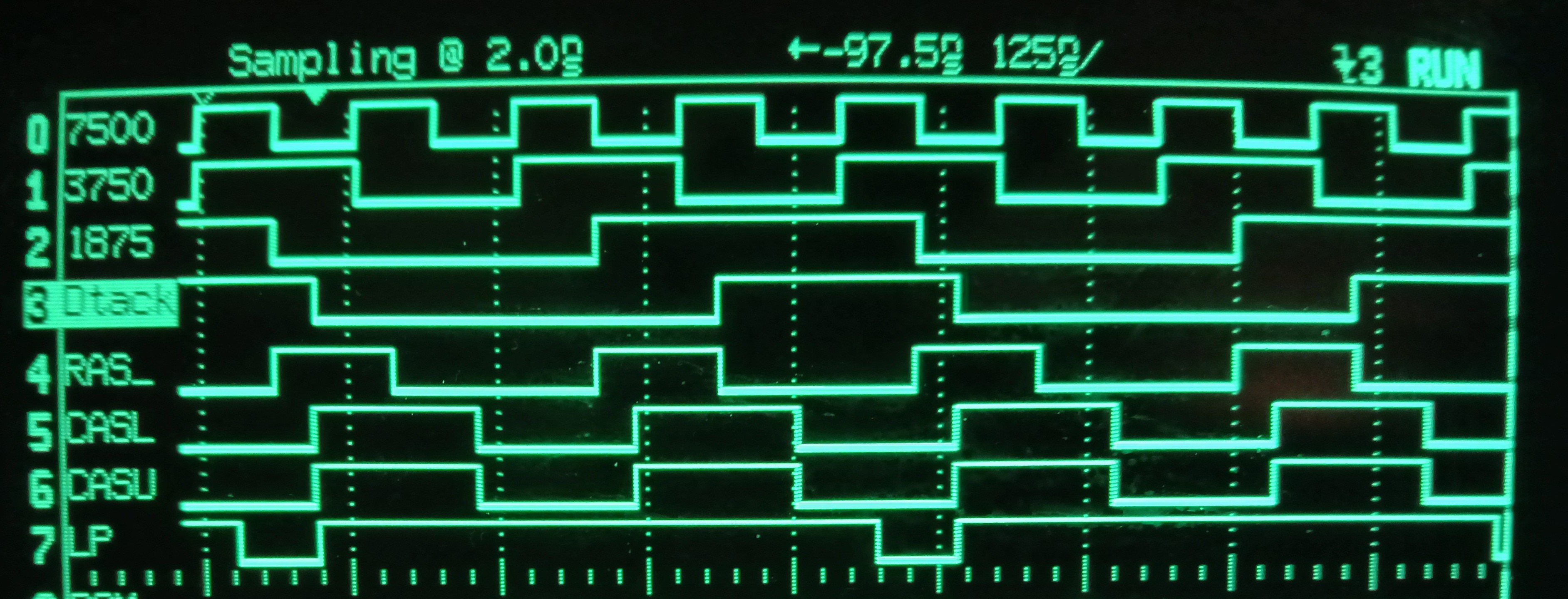
    Having a look at the outputs of the timing GAL, things look as expected. The 15 MHz clock in is divided to 7.5 and 3.75 MHz. This is divided again to 1.875 MHz, slightly delayed, to be the CRTC character clock (CCLK). 

    The /RAS, /CASL, /CASU and /LP signals have the right timing relationship. The image below shows the video accesses reading upper and lower bytes at the falling edge of CLCK. It is okay for /RAS to rise before /CAS, this does not end the cycle early.

    /DTACK is only used to tell the CPU that data is ready. The CRTC is synchronous and runs whether data is ready or no. So /DTACK is idle for video access.

    Video cycles only:

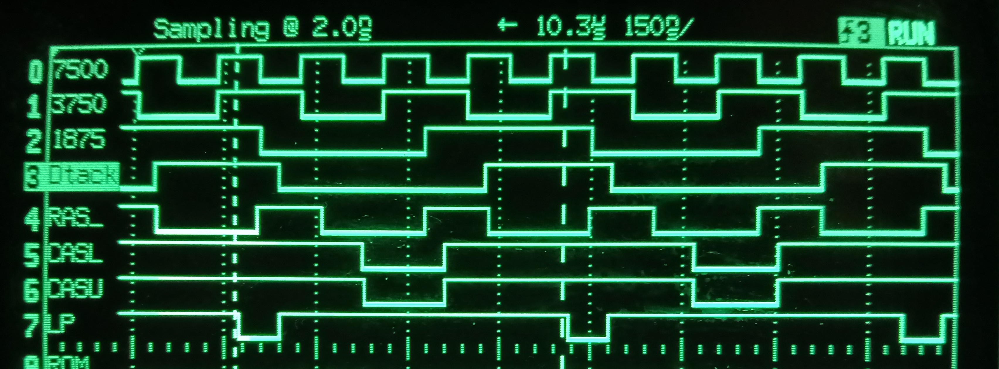
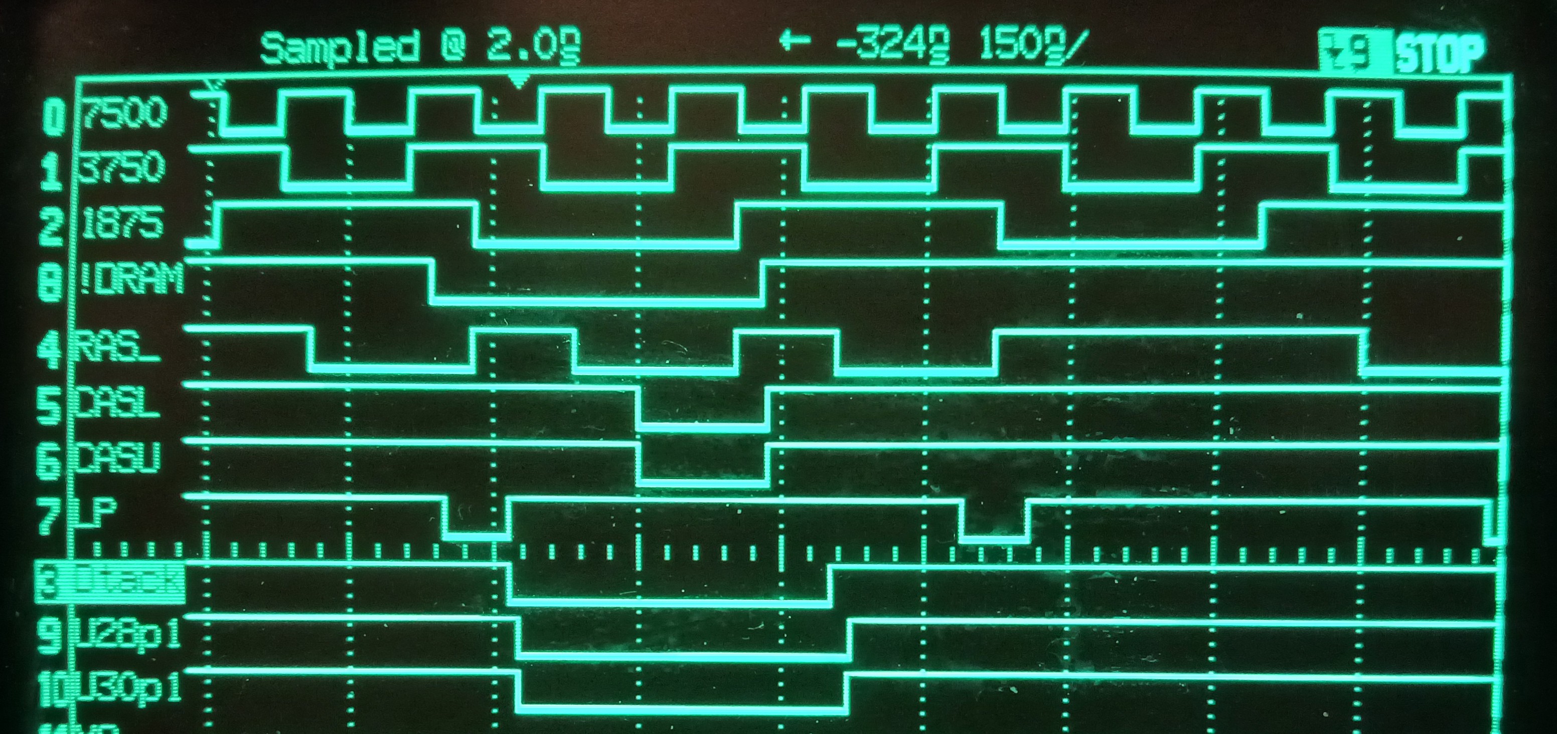
    Now let's set the trigger to /DTACK, which is the timing GAL telling the CPU that data are ready.

    CPU cycles:

    Here we can see CPU accesses taking place. Again this looks good, /DTACK is low during /RAS and /CAS of the CPU access.

    Both cycles:

    Here we can see both CPU and video accesses taking place. Again this looks good, /DTACK is low during /RAS and /CAS of the CPU access.

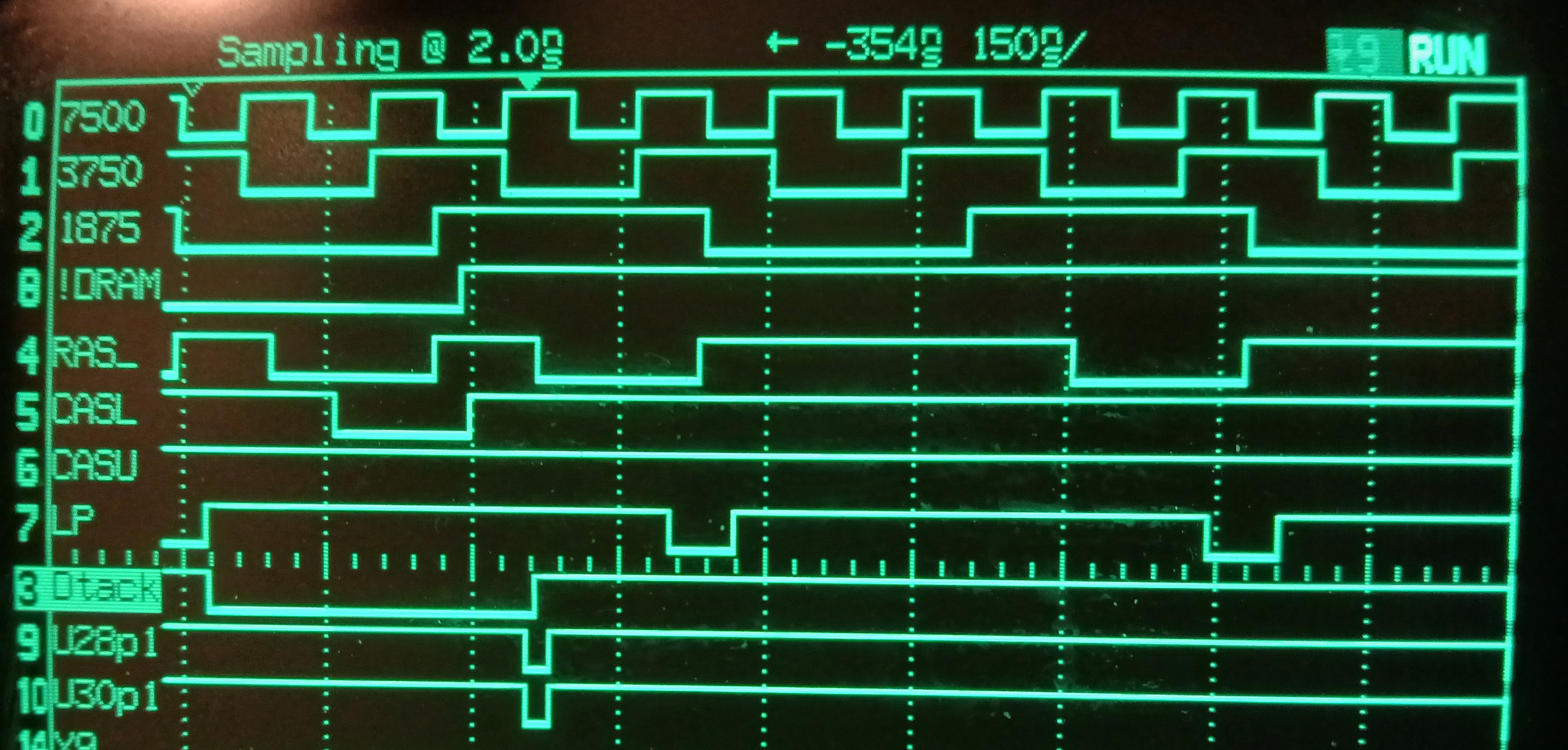
    DRAM Data Bus Enables

    Sometimes they are long, like this:

    I'd say these were normal. This looks like a CPU reading 16 bits.

    Often they are very short, like this:

    In the image above, only /CASL is asserted, so the CPU is accessing a lower byte. And writing, because /BDRE (U28 pin 1) is high. The data bit are written to the RAM while /CAS is low, so the brief /BDRE pulse should cause no conflict. I'd say these are glitches, but harmless ones. 

    Replacing the NMOS SCC with a CMOS SCC did not improve things, apart from reducing the current drain to 1.1 amps.

    I fitted a 1000u cap in C2, it did not fix anything but it did allow the 30 MHz oscillator to be fitted and run without glitching. I also noticed the screen would sometimes resemble (with many errors) the proper sign-on screen or formatted output (before being overwritten).

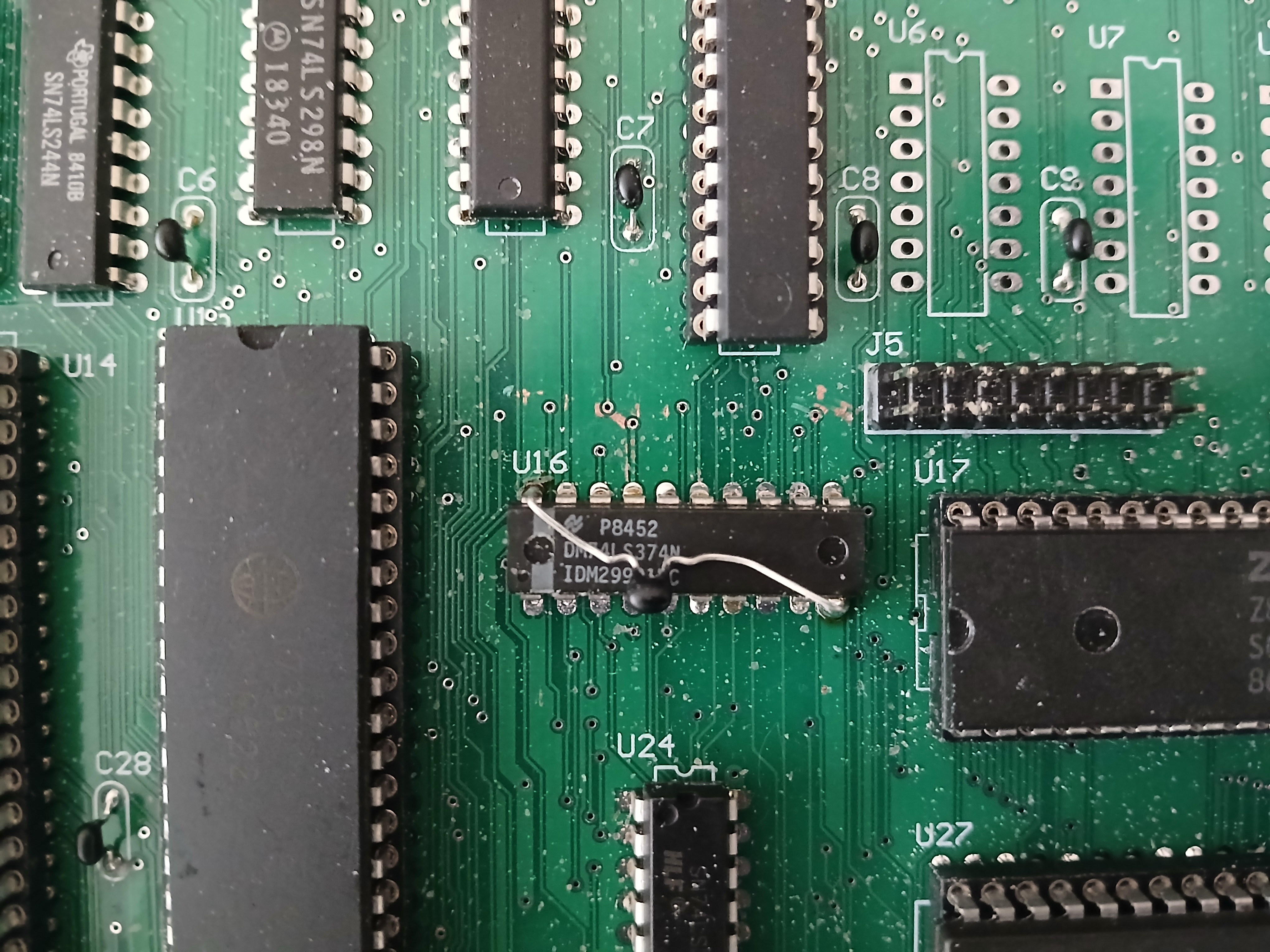
    Decoupling seems to be very sparse. There are no 100n decouplers for the CRTC and SCC which are the most current-hungry chips, judging by their warmth. The CPU and the 6522 VIA have only one 100n cap between them. U16 and U24 have no decoupler at all.

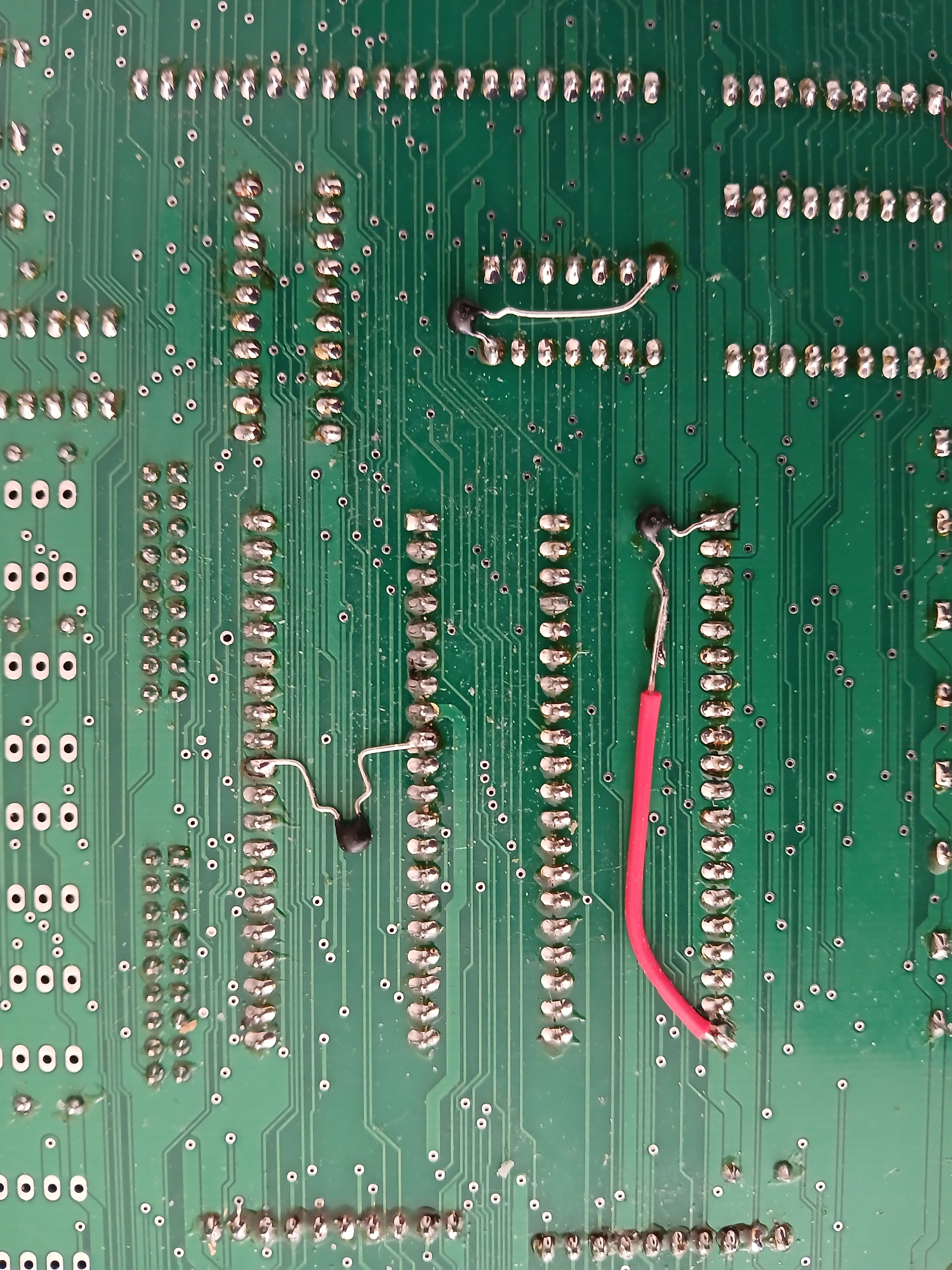
    These caps added underneath:

    This cap added on top:

    This did not cure the problems. Usually just crashed with random garbage on screen.

    Sometimes I got what looks like a top line of garbage:

    Possibly text:

    Or several lines of text:

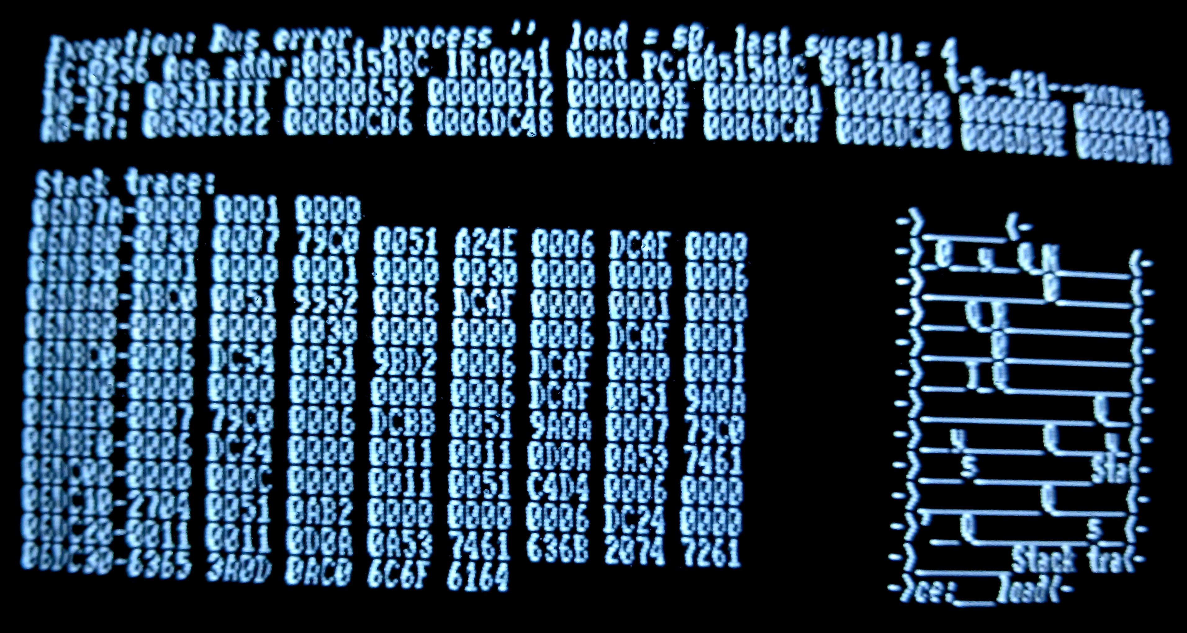
    I'm guessing this one is some kind of register dump. Registers on the 3rd and 4th rows, flag dump on the right of the 2nd row. Perhaps users with working machines can recognise what this screen is. AI suggested it to be a Motorola 68000 exception crash dump screen with something like this kind of text:

    Exception: Address Error      SR=$2700  PC=$00014B20
    Vector: 03  Instruction: 4E73   (Note: S=Supervisor, I-L... )
    D0-D7: 00000000 0000FFFF 00000000 00000000 0001C120 000021A4 00000000 00001000
    A0-A7: 00FF0000 00001F24 00000000 00000000 0001D1A2 00FFFFFF 0000E000 00FFFE00
    
    Stack Frame:
    00FFFE00: 0000 0001 4B26 0003 4E73 0000 0000 0000    [ ....K....Ns.... ]
    00FFFE10: 0000 1F24 00FF 0000 0001 C120 0000 21A4    [ ...$....... .!. ]
    00FFFE20: 0000 0000 0000 1000 0001 D1A2 00FF FFFF    [ ............... ]
    00FFFE30: 0000 E000 00FF FE00 0000 0000 0000 0000    [ ............... ]
    00FFFE40: 0000 0000 0000 0000 0000 0000 0000 0000    [ ............... ]
    00FFFE50: 0000 0000 0000 0000 0000 0000 0000 0000    [ ............... ]
    00FFFE60: 0000 0000...
    Read more »

  • Sequential start-up tests

    Keith07/30/2026 at 01:03 0 comments

    The original firmware reads SW2 and performs either 1 of 8 primitive tests, or 1 of 8 running modes.

    The tests rely on output ports to indicate information, but that requires some LEDs to monitor the states which might be pulsing rapidly. I feel this is rather unsatisfactory.

    In a previous job, I worked for a smart card company. Smart cards are small but highly critical single-chip microprocessor systems. Any bugs would be disastrous, so checking smart card security costs literally millions of pounds. I only know a hand-waving amount about they work, but the start-up process is useful.

    I propose this start-up test sequence:

    • Check registers work
    • Check the ROM contents have a valid checksum
    • Check the CRTC is present (write/read a register)
    • Initialise the CRTC (so that RAM gets refreshed)
    • Check the VIA is present (write/read a register)
    • Set the video colours
    • Check the stack RAM is working (so you can use it for subroutines)
    • Check the SCC is present (write/read a register)
    • Check the video RAM stores data written to it
    • Send failure report to the screen or serial port
    • If no failures, boot up as normal

    It could write a digit code to the output port to indicate the last test that succeeded, or a binary pattern showing which ones had succeeded or failed.

  • Flash ROM issue fix

    Keith07/27/2026 at 17:37 0 comments

    When examining the piggy-back SRAM idea, I noticed the original design used this wiring:

    R/!W --> inverted --> ROM !CS
    ROMSEL --> inverted --> ROM !OE

    This was a way to reduce EPROM access time. It would be activated early on, and then take only the shorter output buffer switch-on time to provide the data when selected.

    Flash ROMs are not exactly like EPROMs, because they want the address to be stable while they are selected. If not, they internally start accessing a garbage address then try restarting when the address changes. With the original wiring, every read cycle will start an access. 

    This probably explains why start-up tests that didn't involve the DRAM were not reliable. Most of the time, a test would run for seconds, but then crash.

    At this point, I could either try using a 32-pin EPROM, or try swapping the !CS and !OE wires over.

    This would ensure the address is always valid (!AS asserted), and as a bonus the !OE signal could be shared with piggy-backed SRAM chips.

    I only have 28-pin EPROM chips so I'd have to modify tracks. And if I have to do that, I might as well save a step and modify tracks to suit the Flash ROM.

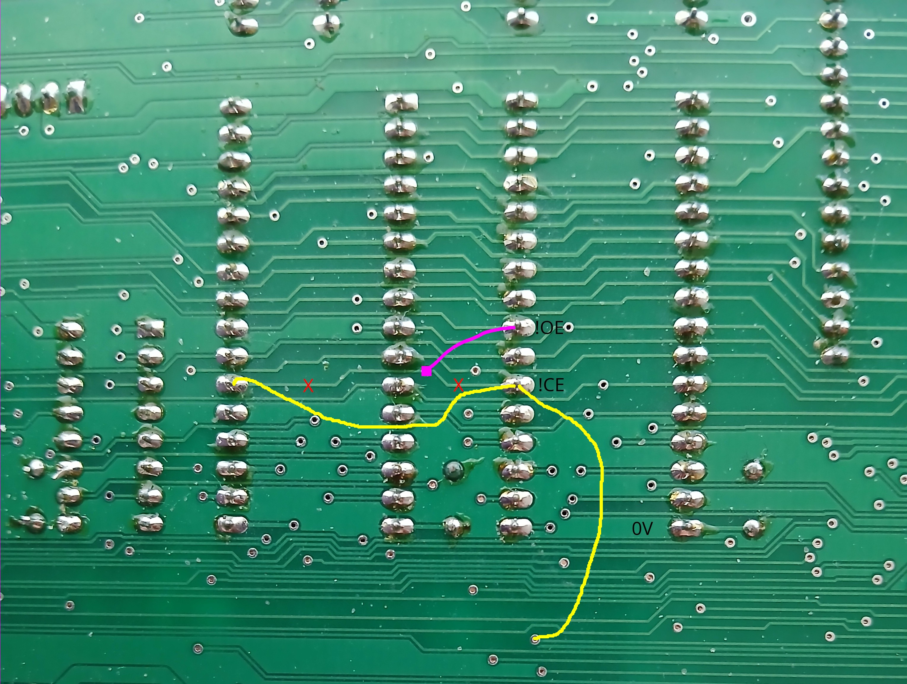
    Here are the mods to be made on the underside:

    Cut tracks at the red Xs, then make the purple wire.

    This isolates the pin signal from !CE and routes it to !OE.

    Now we need to isolate the signal that goes to !OE and route it to !CE.
    Make the yellow wire to drive !CE.

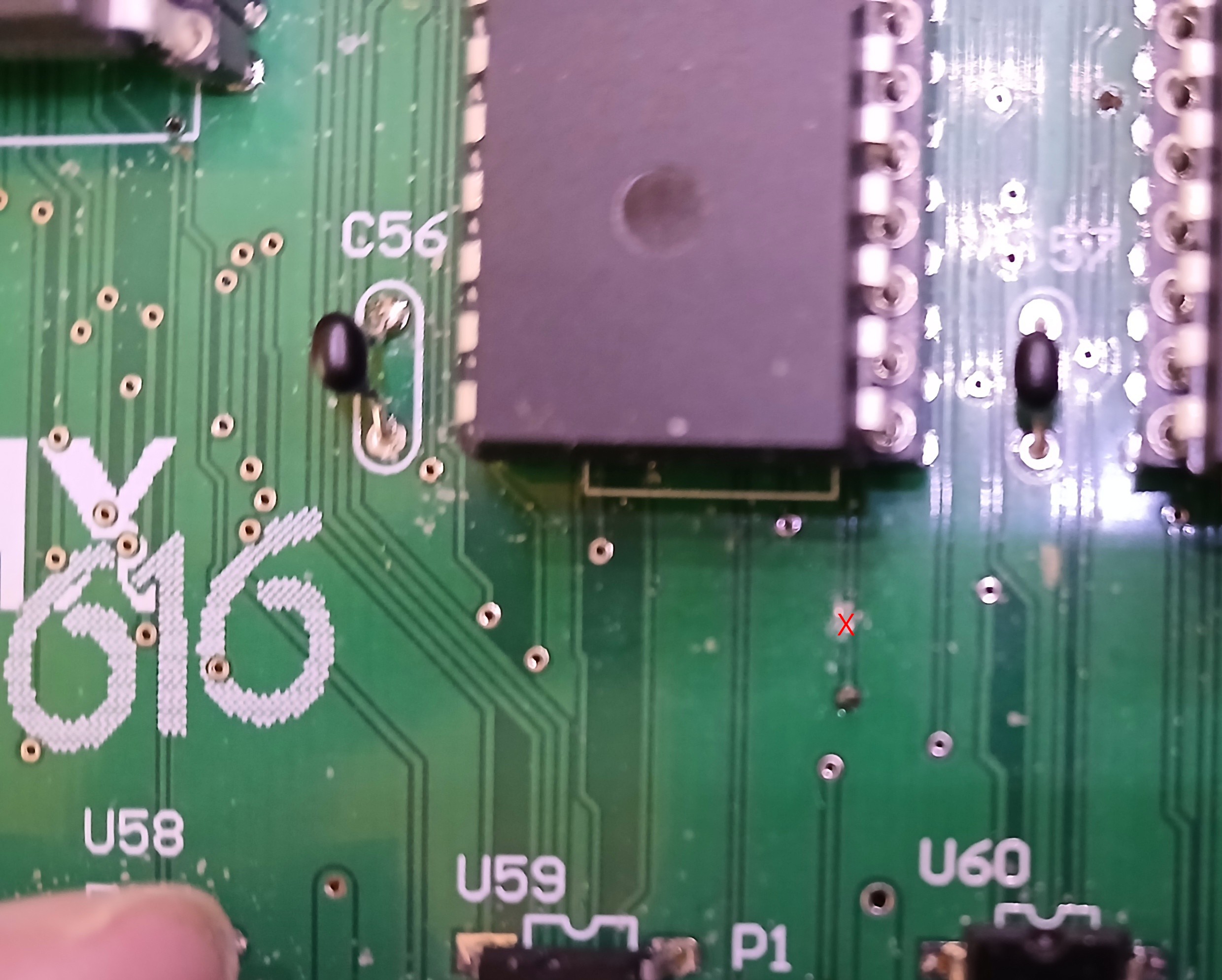
    Then turn over and cut the track marked with a red X.

    Switch on, some tests running.

    0 pulsing. Screen shows gradient of grey, because VIDLATCH increments background colours.
    2 CRTC not initialised. LED pulses (VIA test)
    4 CRTC not initialised. LED pulses (Iporttest)
    6 CRTC not initialised. No pulsing so fail (memtest fail)

    1 CRTC initialised. No pulsing so fail (SCC test)
    3 CRTC initialised. No pulsing so fail (Crtcrwtest test)
    5 CRTC initialised. No pulsing so fail (RAM test fail)
    7 CRTC initialised. No pulsing so fail (screen RAM fail)

    When the screen is initialised, it is just DRAM garbage, no characters.

    Run mode (15) is a little better than before, because it does appear that the screen RAM is being written to, however this does seem random so I assume the software is running amok.

    So I thought the ROM behaviour had improved but the RAM is still failing.

    Then I checked the Exception report, it says the last instruction was in ROM.

    ROM changed to Atmel 29F002T-70 chips, but these worsened the issues if anything at all.

    UPDATE:

    The original design swapped the signals over, but Jo's modern design does not. So all the mods I made above had to be undone! 

    The swapping probably only needs doing if you are upgrading an original board to use Flash ROM. I have not got an old board so I cannot check this out.

  • Piggy-backing SRAM

    Keith07/26/2026 at 13:37 0 comments

    All pins compatible except:

        Skt.    RAM
    31    PU    A15 wire to A15 on skt pin 29
    29    A15    !WE flying wire to CPU.9, TPAL.8, U55.12, or U54.13
    24    !OE    !OE wire to Skt. 22 (which is !RD)
    22    !CE    !CE

    ROM.!OE is !ROMSEL

    ROM.!CS is labelled BR/!W on circuit rev. A, and /R/W on  circuit rev. B.
    The circuit shows it is inverted CPU R/!W, so it is more of a shared !RD signal.
    That makes sense, but intuitively I would have expected the !RD to go to ROM.!OE and !ROMSEL to go to ROM.!CS.

    Maybe OE access time is faster than CS?

    Now the SRAM needs activating at the bottom block, I need to activate it there.

    /RAMSEL is actually /DRAMSEL, it goes to TPAL.3 to activate the DRAM signals.
    So I removed the link between pins 1 and 2 of link area P1 to disable the DRAM there.
    To disable it everywhere, it would need a pull-up resistor.
    So instead, I shall enable it just before the ROM.
    IC59 decodes memory into eight 1-megaword blocks.
    Two 512K SRAM chips would appear twice in a block.
    I shall relocate the DRAM to block 4 at 0x400000, 
    so that it is safely driven high.

    A23 22 21 20     
    0   0  0  0    !SRAM
    0   0  0  1
    0   0  1  0
    0   0  1  1
    0   1  0  0    !DRAM
    0   1  0  1    !ROM
    0   1  1  0    !IOSEL
    0   1  1  1    !EVPA

     Next issue will be to drive the CPU !DTACK when SRAM is accessed.

    One could do this by pulling the !EXTDTACK signal low.

    This is the open collector signal from external devices on the expansion slots.

    I don't have any expansion cards, so until I do I can wire the !SRAM signal straight to !EXTDTACK.

    The system should then be able to boot up using SRAM.

    No video, so it has to use the serial port as a user interface.

    The DRAM should still be accessible for testing.

  • Switching on

    Keith07/15/2026 at 18:57 0 comments

    2026-07-15

    All chips for minimal system in. 

    Power, ground and all chips on the left of the 6522 seemed shorted when buzzed, but hi-z when resistance measured. Multimeter battery measured 2.2 volts, so changed for fresh and the buzzed-shorts went away.

    Applied power. No magic smoke. Power LED on. Current draw is 1.16 amps (CMOS CPU fitted).

    Next step: apply logic probe to check signals that should be pulsing are actually pulsing.

    Frequencies on pins 17, 18 and 19 of the timing PAL are correct.

    Frequencies on the CRTC chip:

    VSYNC (40) = 50 Hz
    HSYNC (39) = 15.625 kHz
    DE (18) = 10000 = 200 * 50 Hz
    CCLK (21) = 1.875 MHz

    DRAM /RAS (4) = 1.841 MHz

    So it looks like the system got as far as running the code in the ROM to initialise the CRTC.

    Next step: Check the video output.

    2026-07-16

    Kludged a phono socket on, fed it to a small TV.

    And here is the video:

    The startup switched are all open, selecting video with minimal RAM disk.

    If switch 4 is closed, selecting serial port, the video is not initialised as above. If the RAM is not working then it probably won't be able to call serial I/O subroutines properly.

    I'm using a 29.5 MHz oscillator so the timings are proportionally slower, and these small tellies never had great timing.

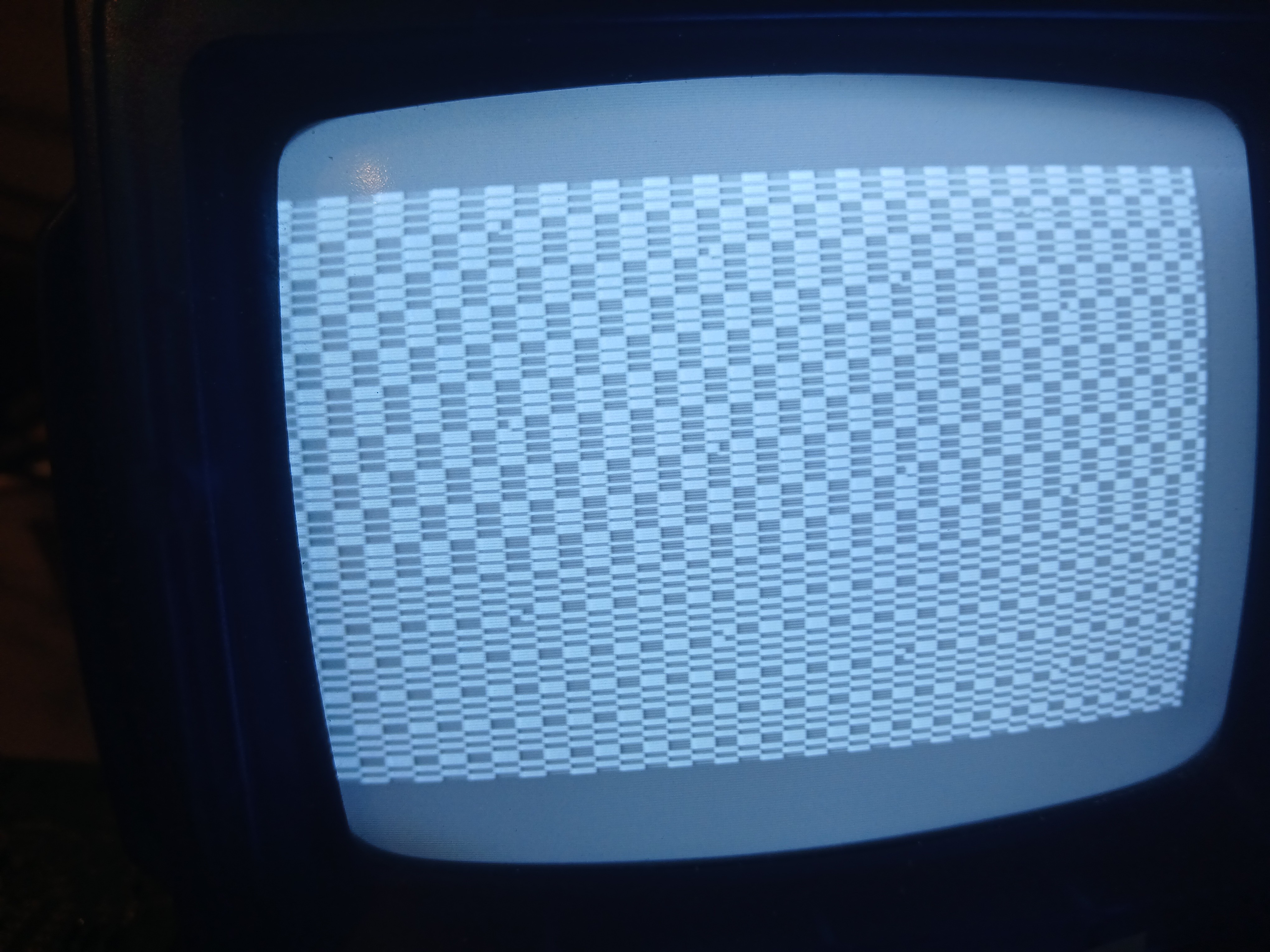
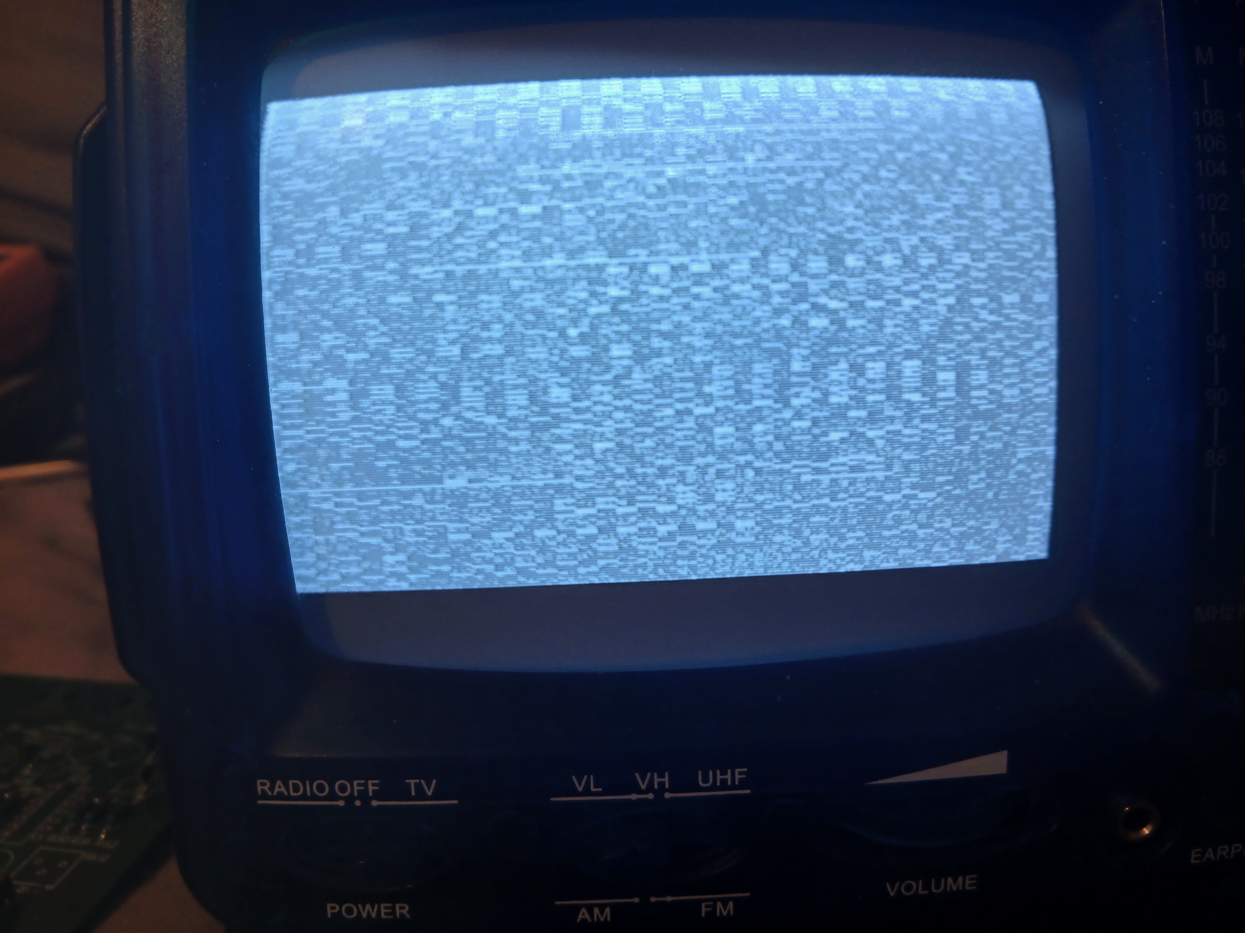
    Looks like the CRTC has been initialised, but not the video RAM. The video patterns look like DRAM start-up. 

    Removing or swapping the ROM chips has the same effect, no video. So I believe the CPU is waking healthy enough to program the CRTC.

    If all RAM chips are removed, the pixels are all white. Which suggests the DRAM bits are being read and the shift registers are working.

    Removing all the RAM chips, and shorting individual data outputs to grounds should produce dark narrow vertical lines. It does for most, but not IC47, 73 and 74.

    I then notice I have 18 RAM chips, not 16. IC47 is listed as a spare, and IC74 is not listed at all so presumably this is a spare too. So that leaves IC73 suspect. If pin 14 is connected to a known-good ground, the vertical stripe appears so it is connected to the shift register. Pin 16 is not connected to ground. 

    Visible bad joint corrected, but behaviour is like before. Occasionally there is flickering of the background, perhaps random writes to the background colour register. 

    I also sometimes get this screen mode:

    2026-07-17

    I fitted a LED in JP3 and U18 which drives the LED. 

    Test results:

    Test 0: 

    Centronics latch pin, DAC latch pin, Video latch pin, Analog multiplexer latch pin (Relay coil control, LED), all pulsing low.

    Fails with bus error if PCB flexed. Address pins go hi-z.

    Test 1: SCC

    U64.12 pulsing low. LED pulsing for a while. 

    Fails with bus error if PCB flexed.

    Test 3: CRTC. Blinks LED.

    Test 4: IPORT. Blinks LED.

    So far, so good. Now the failures.

    Test 7: No LED blinking, but that is normal.

    Tfails to increments border and screen colours in 320 mode, or display character set in 640 mode, or draws coloured line test pattern in 320 mode.

    U64 (an LS139) pins 2, 3, 13, 14 pulsing low (A8, A9). Pins 4,5,6,7, 9,10,11,12 all high because pins 1 and 15 are high. No I/O devices are being selected. /AS, /UDS and /LDS are active, but not accessing DRAM. It is looping in ROM.

    Test 2: VIA pin 23 /CS pulsing, but only for a few LED pulse cycles.

    Test 5: Read / write memory: LED pulsed for 8 cycles. Bus error (U33 pin 5 low).

    This test does not even start LED blinking if the previous test 7 was run and a soft reset done. 

    Serial port tests

    I attached a USB-to-TTL-serial cable. 

    Test 1: LED blinks but no serial port traffic. 

    Looking at the code, the SCC test is very primitive, it just reads and write a byte to the SCC. It does not initialise the SCC to open a communication channel.

    So now I am wondering what to do. 

    I suspect that the dual-ported DRAM is at fault, being the most...

    Read more »

  • Video options

    Keith07/13/2026 at 12:43 0 comments

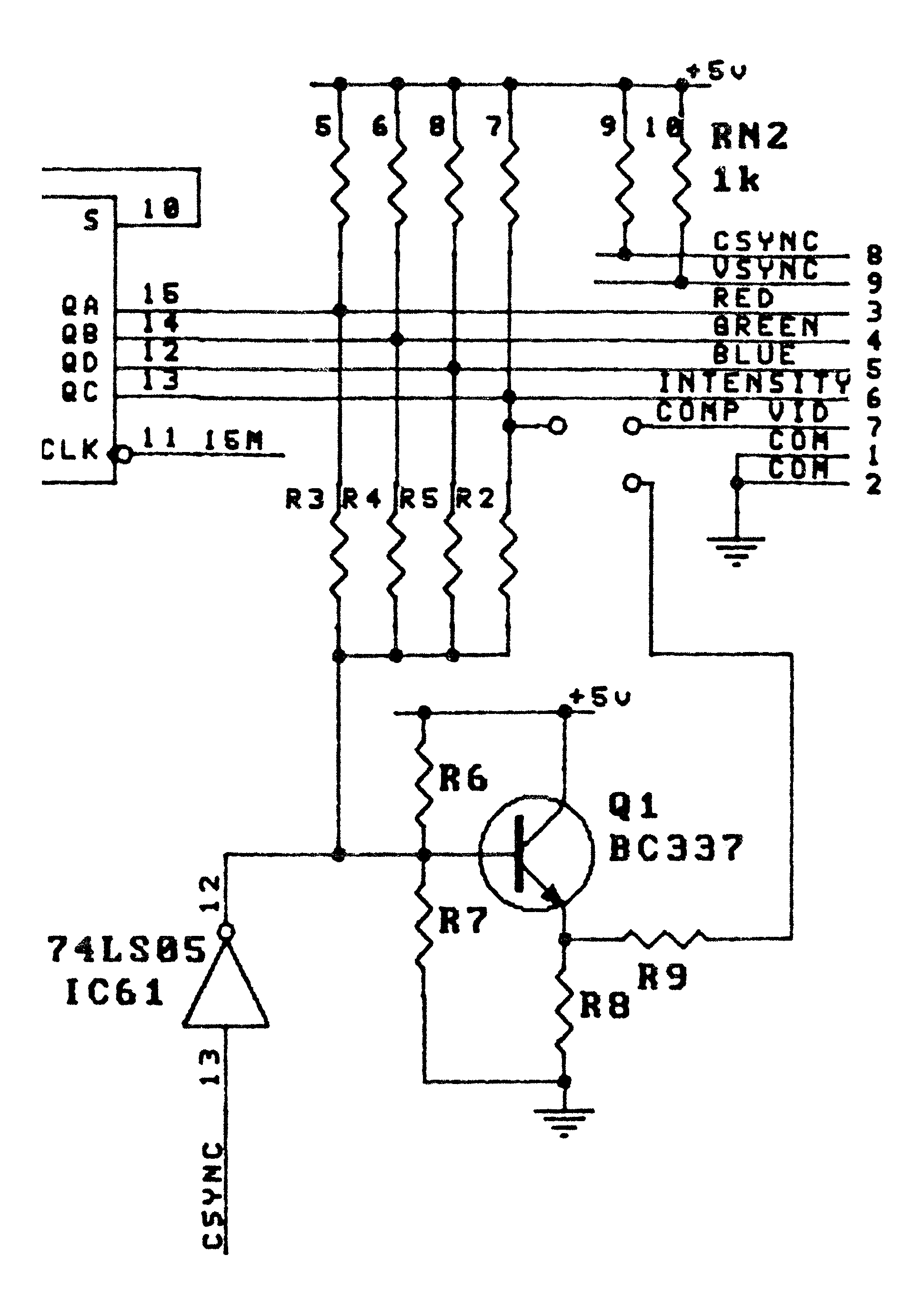
    My first though was to put some resistors in series to drop the 5V RGB signals to 0.7V and feed them into a SCART socketed TV.

    The RGBI and CSYNC drive a resistor DAC, but CSYNC also pulls down the RGBI pins a bit. No problem to a digital monitor, which still seems them as logical 1 or 0, but it does affect levels going into an analogue display. 

    Computer designers never seem to be good at video circuitry.

    The connector pinout is the same as the CGA standard but I don't want a bulk old monitor around, even if I could obtain one.

    I only want to check the 1616 is alive. Composite video seems the least effort and simplest cabling. 

    I'll design some decent video circuitry some other time.

View all 28 project logs

Enjoy this project?

Share

Discussions

kdhildred5 wrote 04/27/2026 at 07:24 point

aggghhh just realised thats you lol

  Are you sure? yes | no

Dave wrote 04/29/2026 at 06:53 point

He he yes he did a great job with the resto and well documented.

And I sent you a PM, please let me know if you received it. Thanks

  Are you sure? yes | no

kdhildred5 wrote 04/27/2026 at 07:20 point

and this one https://microbeetechnology.com.au/forum/search.php?action=results&sid=d9201b4992e4323fdf8ed3018eb519f1&sortby=lastpost&order=desc

full of software and manuals...

  Are you sure? yes | no

kdhildred5 wrote 04/27/2026 at 07:18 point

hey found this as well https://forum.acms.org.au/t/retrochallenge-2023-10-applix1616-restoration-documentation/503

  Are you sure? yes | no

kdhildred5 wrote 04/27/2026 at 06:45 point

not sure how to add photos in here or if i can

  Are you sure? yes | no

Dave wrote 04/27/2026 at 07:03 point

Hey thats great I'll PM you. As I'm not sure either.

  Are you sure? yes | no

kdhildred5 wrote 04/27/2026 at 06:42 point

searched through my chip stash and found these ROMs 27512 V3.0b H and L (high and low) ; 27256 V1.4a H an L ; SSDDROM V1.4a and V2.0. TPAL1 V51 and VPAL1 V5

  Are you sure? yes | no

Keith wrote 05/09/2026 at 03:05 point

Do you have the actual PAL chips, and if so would you lend them to me?

  Are you sure? yes | no

kdhildred5 wrote 04/25/2026 at 07:12 point

Will check re the PAL's might even have the original ROM as well... did have the 3.5 floppies until a few years back but don't anymore..

  Are you sure? yes | no

Dave wrote 04/25/2026 at 12:54 point

Oh wow ... yeah if you could check that would be great. Thanks :)

  Are you sure? yes | no

kdhildred5 wrote 04/23/2026 at 08:58 point

i remember this. Bought the pcb kit - bare min pcb plus Pals.. Then bought all the chips and soldered it together. Worked first time. Was only the 2nd one I built. 1st was with the RCA1802 processor. Spent hours on that one typing in HEX code just to play Pong. Good days they were. Unfortunately don't have them anymore but I did remove most if not all of the chips from the pcbs. Think they are still in my draws somewhere in IC conductive foam..

  Are you sure? yes | no

Dave wrote 04/25/2026 at 07:04 point

That's cool, it's a pretty complex kit and getting it going first time is an achievement it its self. Would you still have the PALs by any chance? The code to program more no longer exists so looking for these PALs so we can reverse engineer. Then we can replicate them for preservation and to build a complete system. Thanks

  Are you sure? yes | no

Keith wrote 04/14/2026 at 13:36 point

Having merged and hex dumped the ROMs, I found the text:

Applix 1616/OS V4.5a, Compiled: 25th February 1991

  Are you sure? yes | no

Dave wrote 04/13/2026 at 22:16 point

With the mainboard ROMs here what version are they? I believe the last was v45. 

  Are you sure? yes | no

Similar Projects

Does this project spark your interest?

Become a member to follow this project and never miss any updates