Marcellus Pereira
The story behind this project is an interesting one. For various reasons (some accidental, some not), I’ve lost it three times already. From floods that swept everything away to the theft of my CD collection (along with a box of floppy disks).
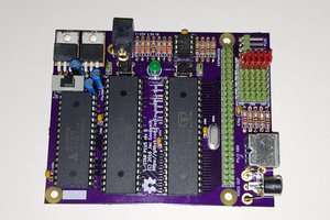
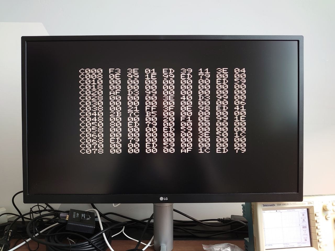
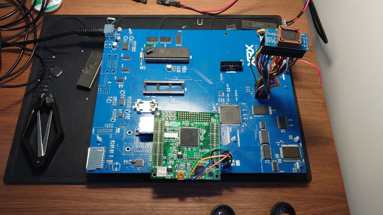
But this time the board is ready and, would you believe it, it’s up and running!
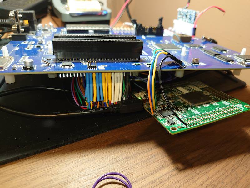
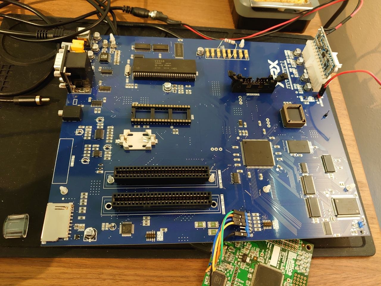
My idea is to have a computer almost as if it had been made in 1994, but using components that are still being manufactured. Unfortunately, the Z380 itself went out of production a few years ago, but as I had a few, I decided to go ahead anyway...
Here are some technical details:
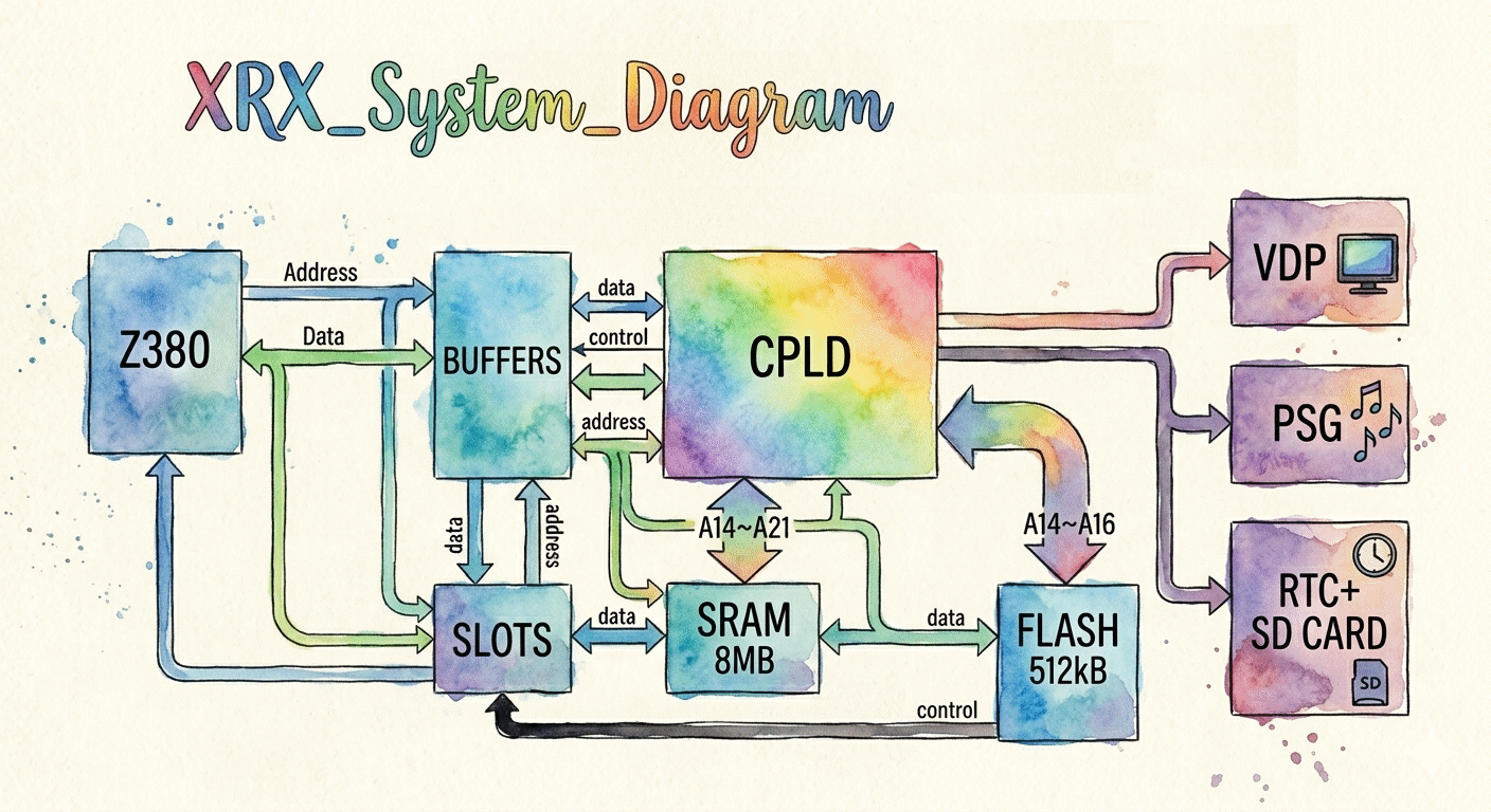
- Zilog Z380 microprocessor
- 14.32 MHz maximum clock speed
- 8MB fast SDRAM
- 512kB Flash memory
- V9958 Video Display Processor
- Composite and S-video output
- AY-3-8912 Programmable Sound Generator
- Mono headphones output
- 2 joystick ports
- 2 MSX-compatible primary slots
- RTC emulated
- SD-Card
- ATX compatible power connector
- mini-DTX board form-factor


 Jac Goudsmit
 Dave Collins
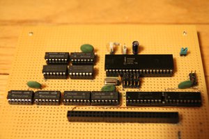
 Bentendo64