Timo
Timo-
Done!
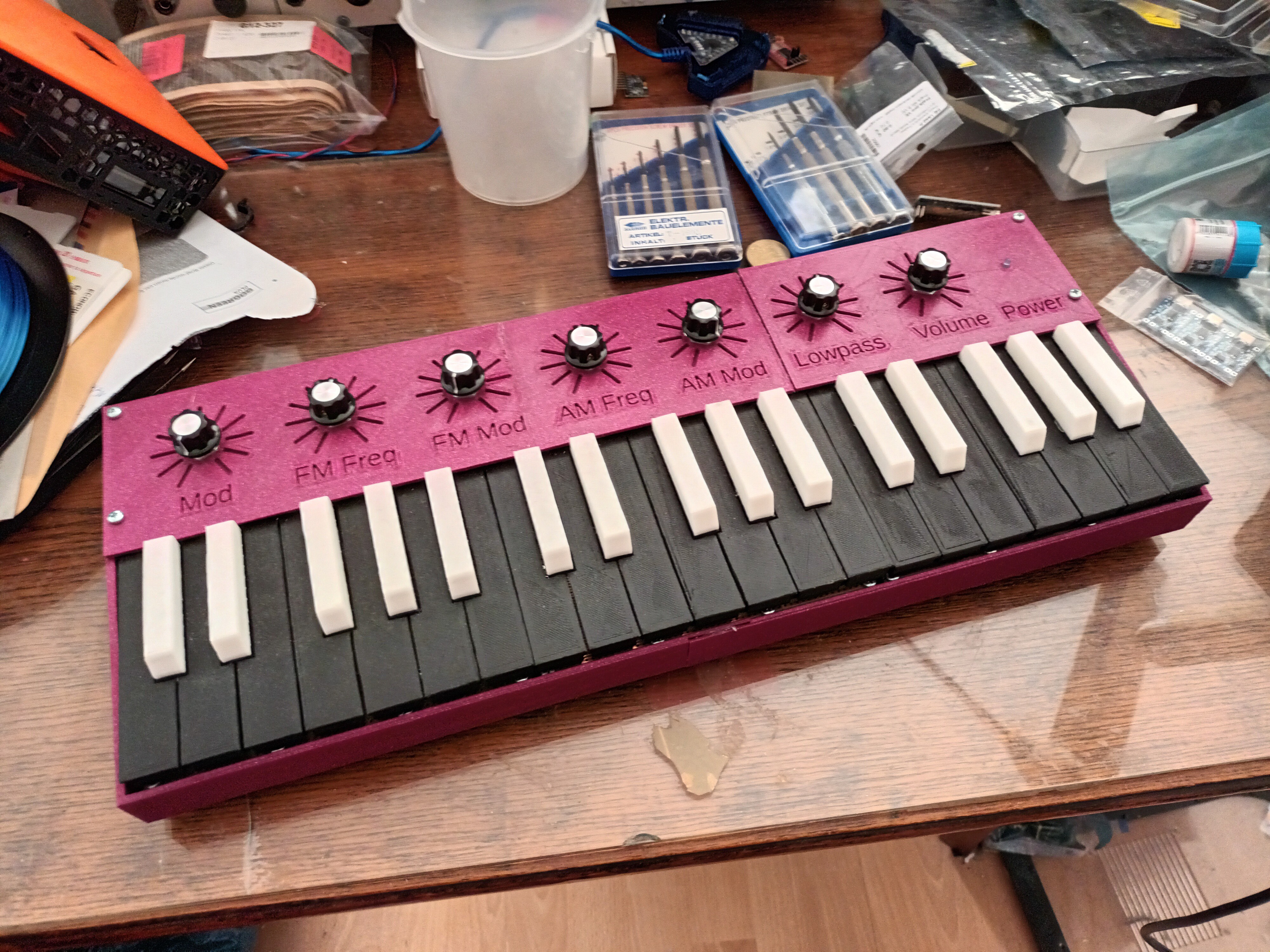
11/27/2022 at 14:18 • 0 commentsIt's done. After two month i finally could bring myself to close the lid.

Fig. 1. A professionally closed lid on a project. Ok , it is done and it works the way it is intended. But is it any good? Short answer: Sound bad, haptic good.
The sound is not good. The only thing i goot out of it was a decent "spooky ghost noise". A rectangle with AM and FM is just not enough to make a good general purpose syntheziser. It is just too simple. After never finishing some way too complex attampts, i over did it in the other direction.
However, the mechanical keyboard itself is quiet nice. If you look at effort vs result, it is phenomenal. It is also very cheap and easy to make and it is very playable. Just some Tact-switches on a pcb and a 3D printed part. It can be used analog (as i did) or just read out digital.
So my final recomendation is: If you need a simple cheap keyboard for your project, copy what i made. If you need a nice syntheziser look somewhere else. But it was still fun to put it together. Note! This is just for the device. The subcircuits work fine.
-
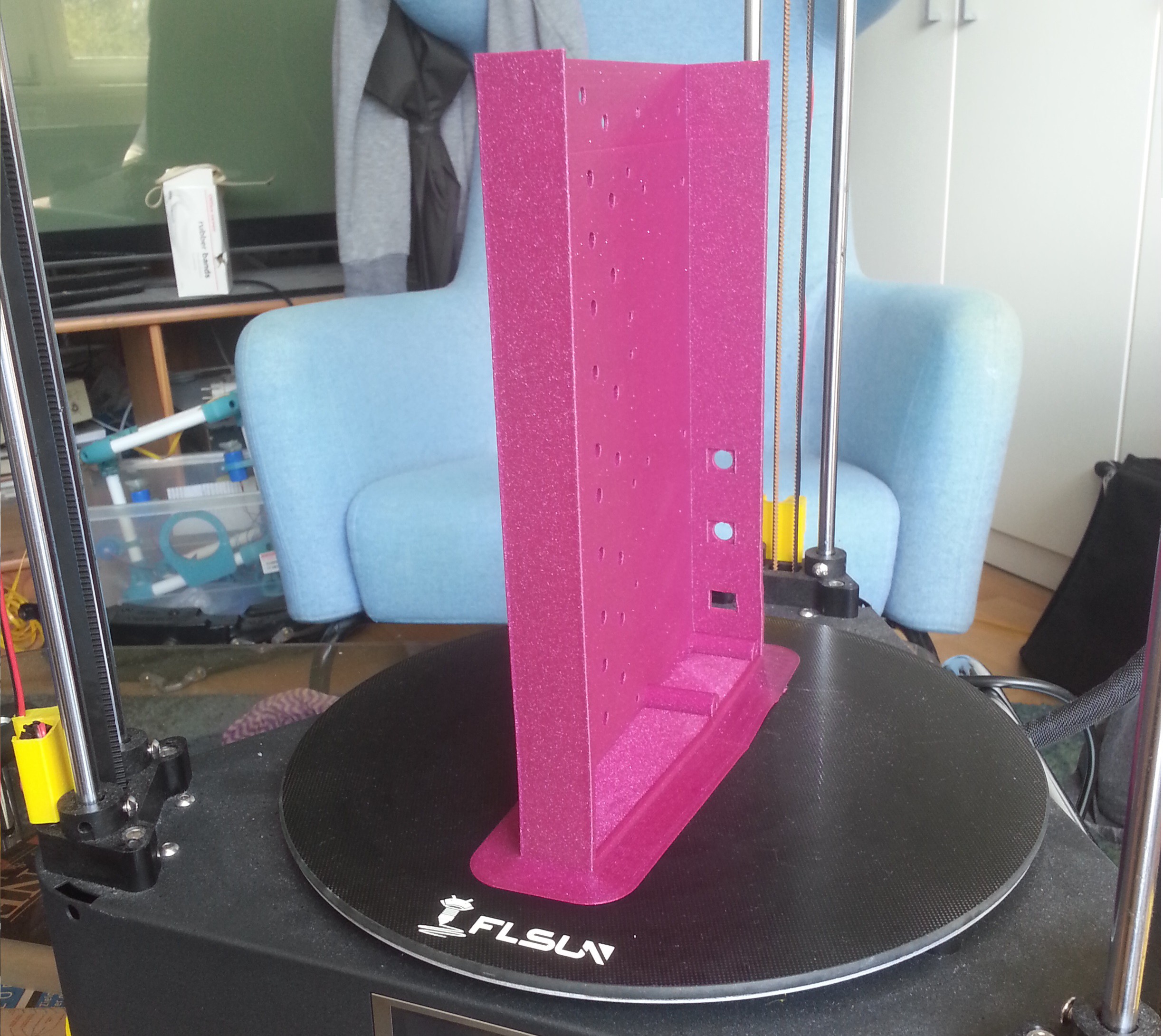
3D printed Case and (almost) final assembly
04/24/2022 at 01:39 • 0 commentsI designed and printed the case for the Synthe555er. Because of the size, it had to be printed it in two parts.
I squeezed everything in the case. In hindsight i should have left some more space between the keyboard, but patience (or violence) is your friend.
Now the only thing that is missing is a propper front panel, some nice poti knobs and documentation .... maybe next time. -
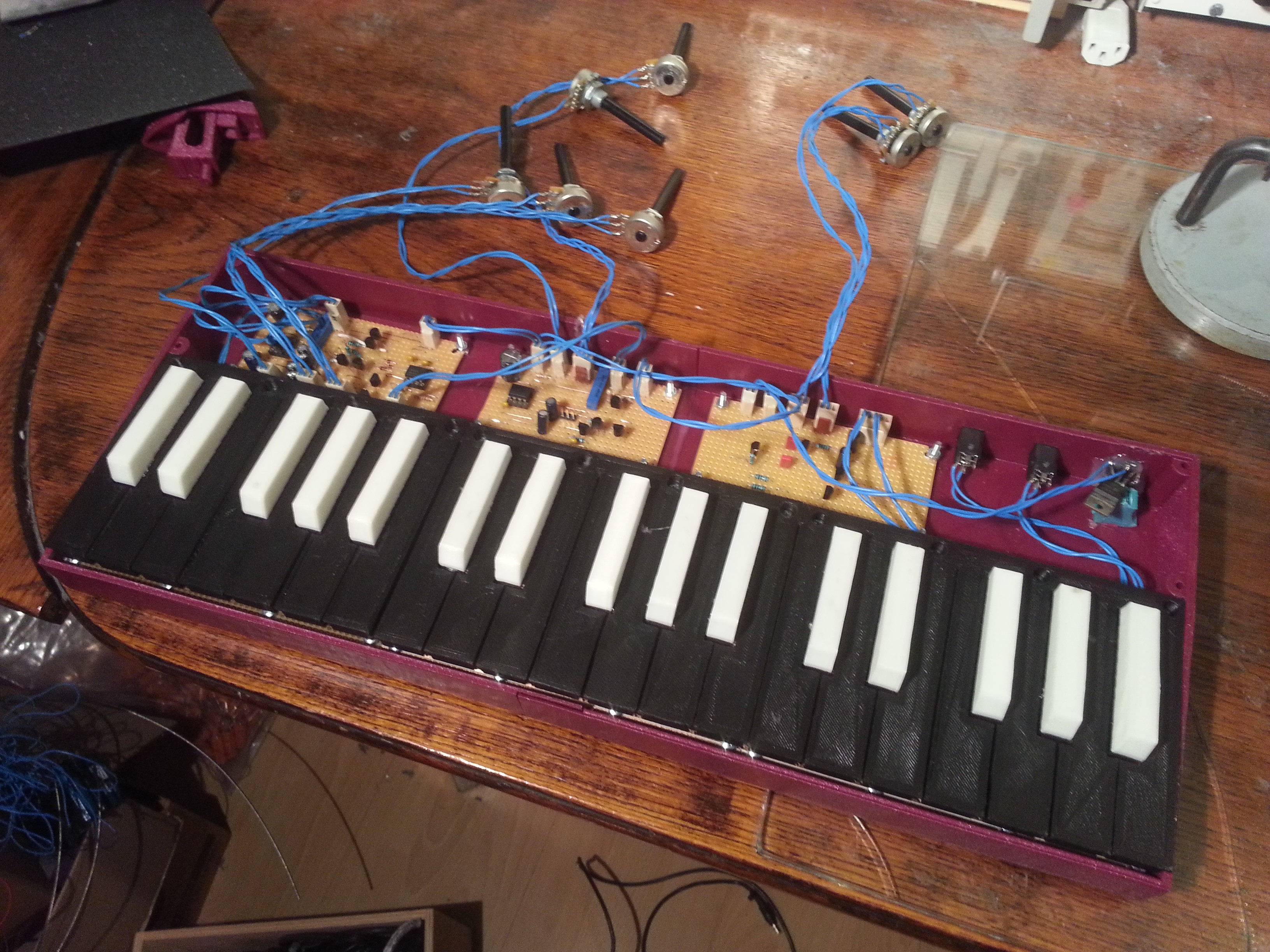
Filter and Keyboard
03/28/2022 at 16:13 • 0 commentsIt has been a long time since something happend here, but in my defence i was very lazy.
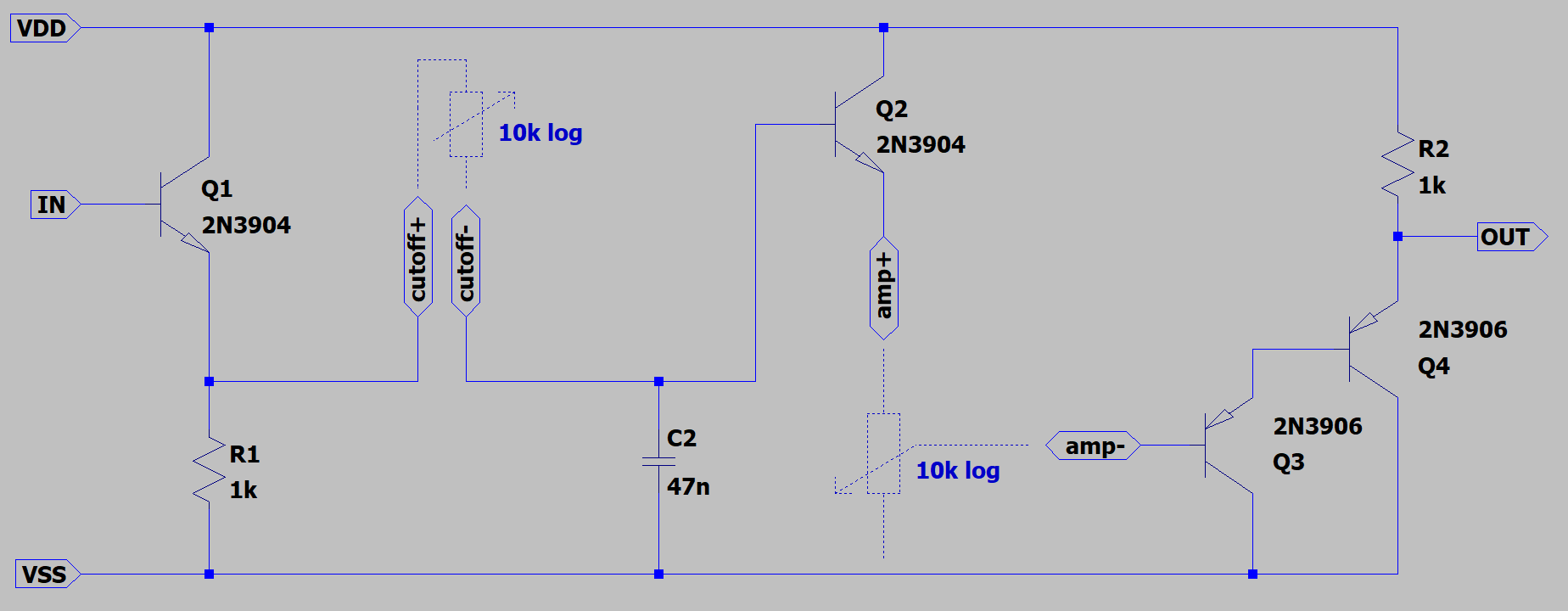
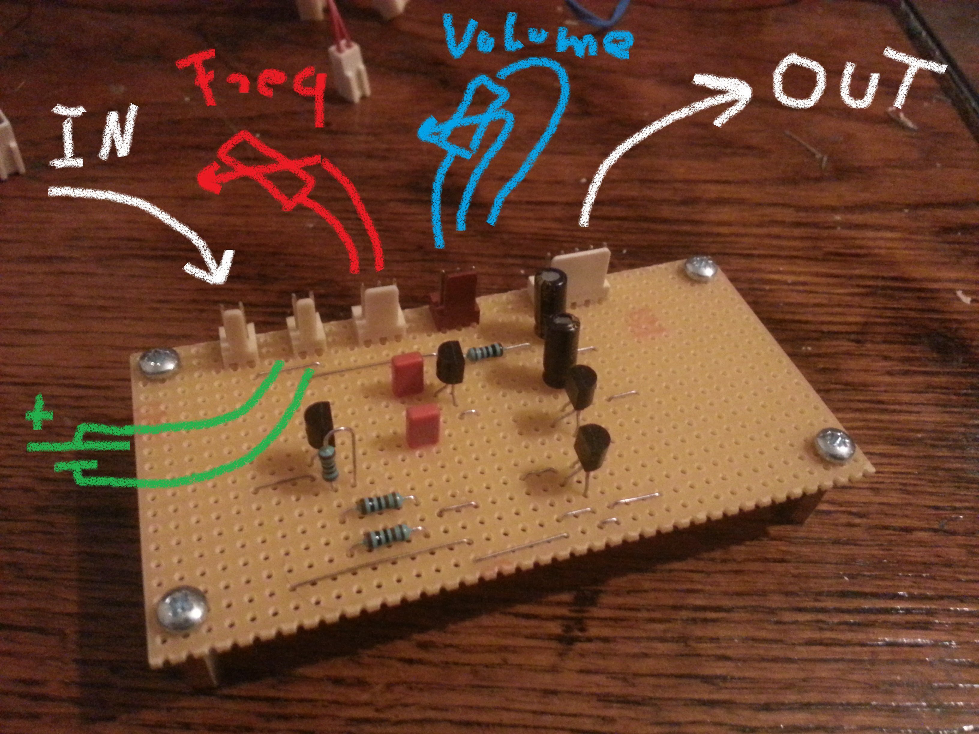
I added an RC lowpass filter and an output driver with volume control to the Synthe555er. This is the schematic, exciting stuff i know.
Again, to keep up with the tradition, there is no NE555 in sight. But i was trying. The original name for this project log was "voltage controlled frequency controlled bandwidth lunacy". Let's leave it at that.
Instead have a look at the finished board:
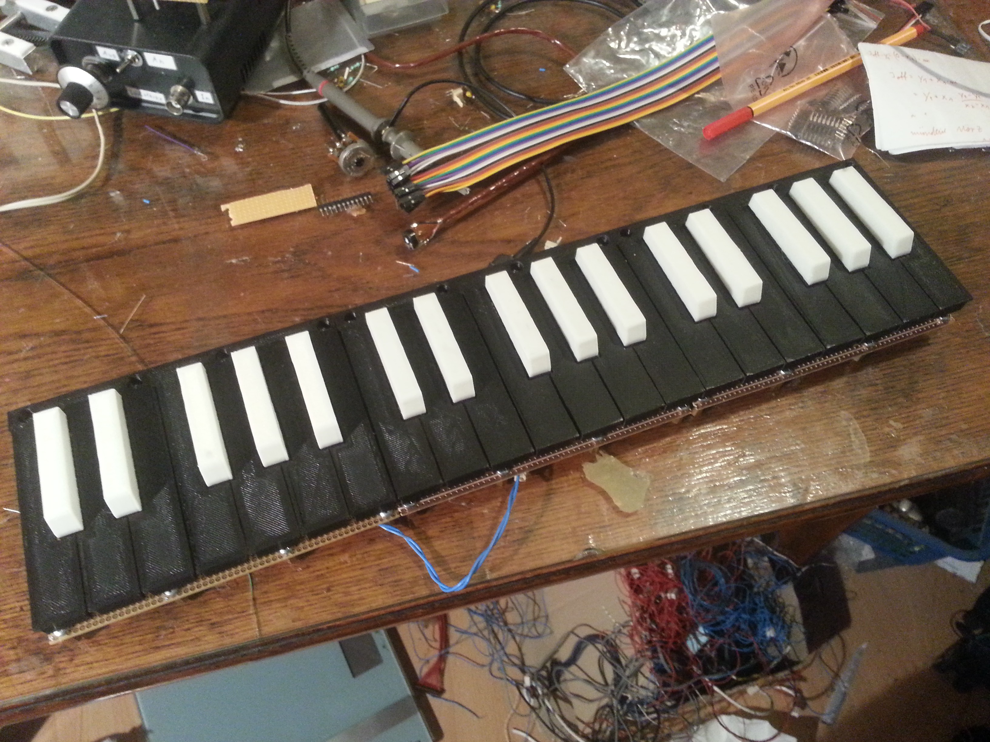
Additonaly i build two extra keyboards. Now i can play three octaves.
-
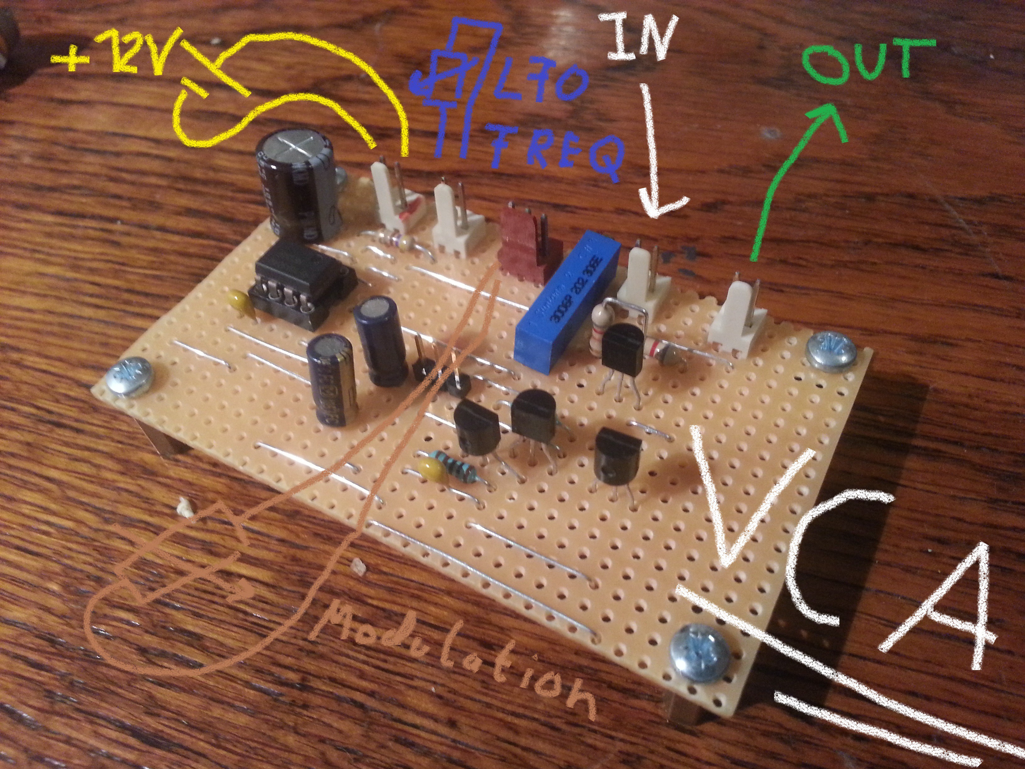
VCA Prototyp and small Bugfix
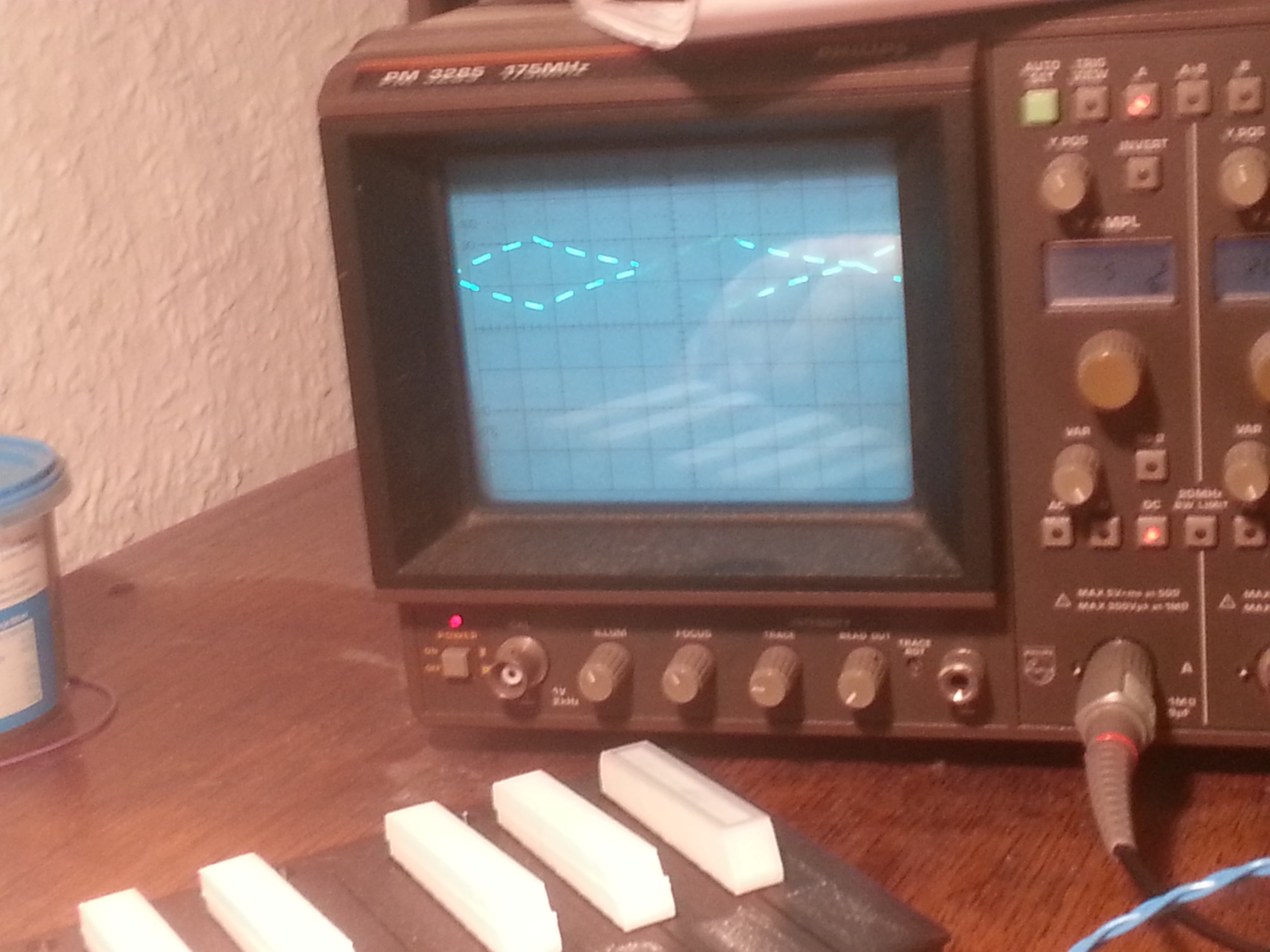
02/24/2022 at 00:05 • 0 commentsThe VCA and it's LFO are finished and they work great.
The resulting waveform can be seen down below. Because of the low frequency of the LFO the waveform is a bi....t hard to capture on camera.
A small bugfix was needed. A revised schematic is shown down below. The input current of Q2 is roughly 10µA. The output resistance of the bias tee which supplys VCA_CV is between 1kOhm and 100kOhm. (Not a great voltage source.) Therefore there is a DC shift of VCA_CV between 0V and 1V depending on amount of amplitude modulation.This results in a noticable lower volume when there is no amplitude modulation. Not a biggy but annoying enought to make me fix it.
Q1 acts as a buffer for Q2. Q1 decreases the input current by its current gain which is roughly 30 in this operationg point.
So far the main components of the Synthe555er are done. But some stuff is missing. Next I will add a simple lowpass filter and buffer to drive a line output or maybe a headphone.
-
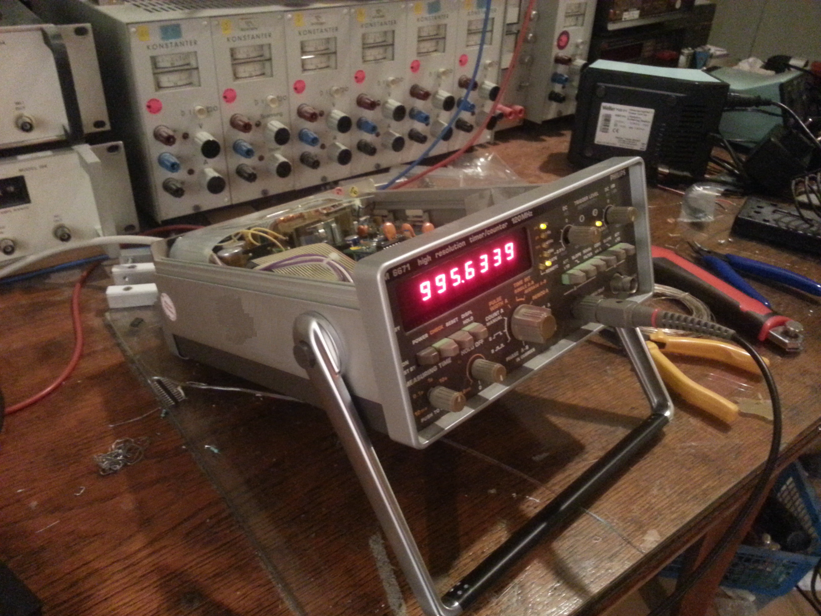
"fixed" the Frequency Counter
02/10/2022 at 23:16 • 1 commentOk, so i have this old frequency counter, which would be perfect for trimming the keyboard but is also kind of dead. When i try to measure a known good source i only get a bunch of zero's and from time to time some flicker.
Luckily there is an easy to obtain service manual with a self test procedure and schematics (Yes they did this in the 80s, crazy right).
So i popped off the lid and followed the manual.- open Device - "Allready did that."
- remove Jumper to get device to test mode - "Easy!"
- set switch on backside to 'use internal clock reference' - "..... Yeah, ... i should do that."
Turns out if you want to use an external reference source you kinda need one ... uppsi.
After setting the frequency counter back to its internal reference it worked great. I wonder if that was the reason why it was thrown out by its previous owner.
-
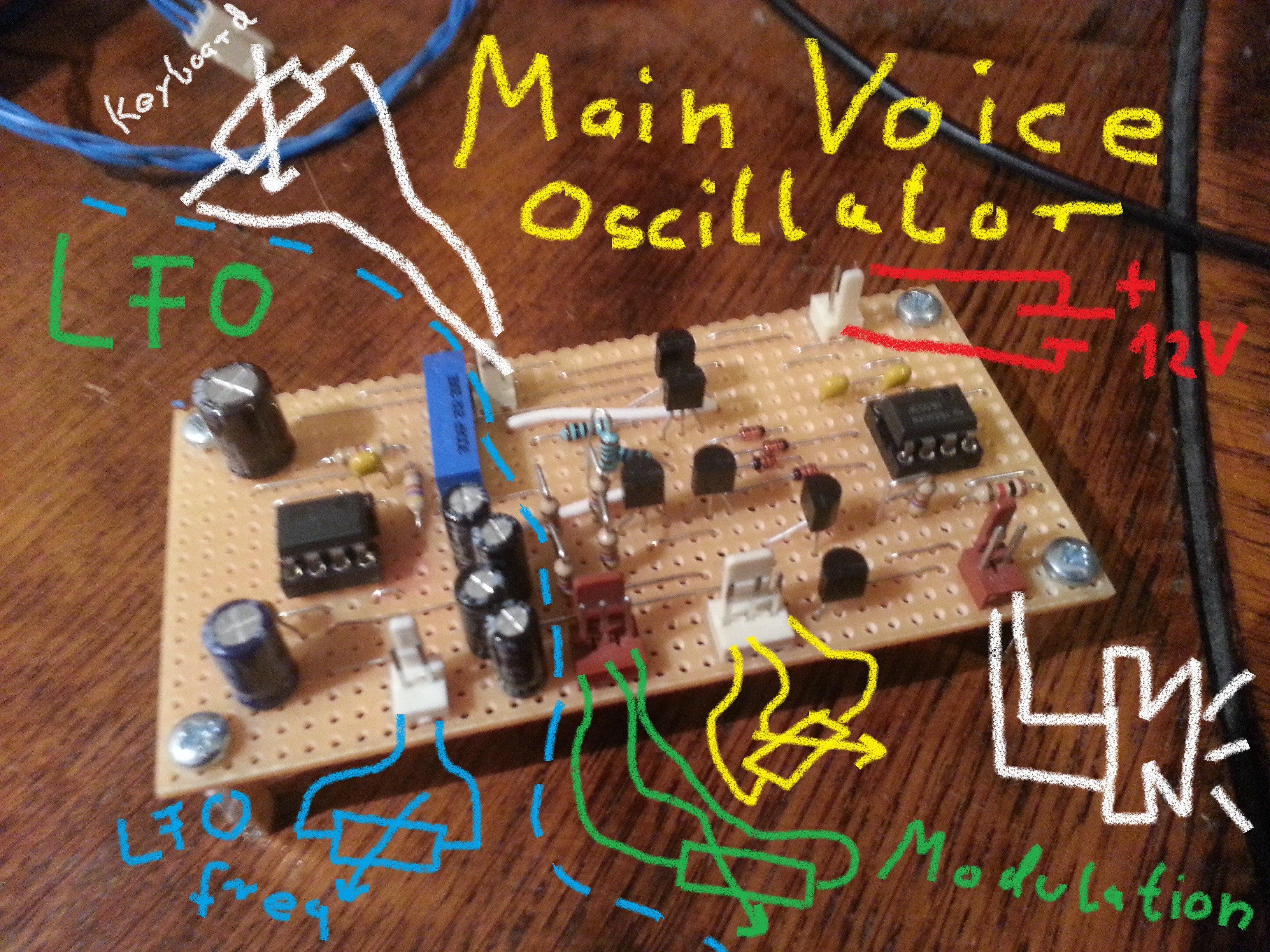
Real Hardware, Main Voice Oscillator and Keyboard
02/09/2022 at 21:46 • 0 commentsFinally some progress on this project. After all these simulations it is time for some real (working) hardware. Enjoy this highly technical drawing:
This board contains all circuitry which is shown in the main voice oscillator testbench (Oscillator, LFO & BiasTee). And beside some changed component values and added bypass capacitors, it's the same schematic. Changes were only necessary because i couldn't be bothered to stand up and fetch the right value. So 480Ohm + 480Ohm = 1kOhm it is.
Keyboard
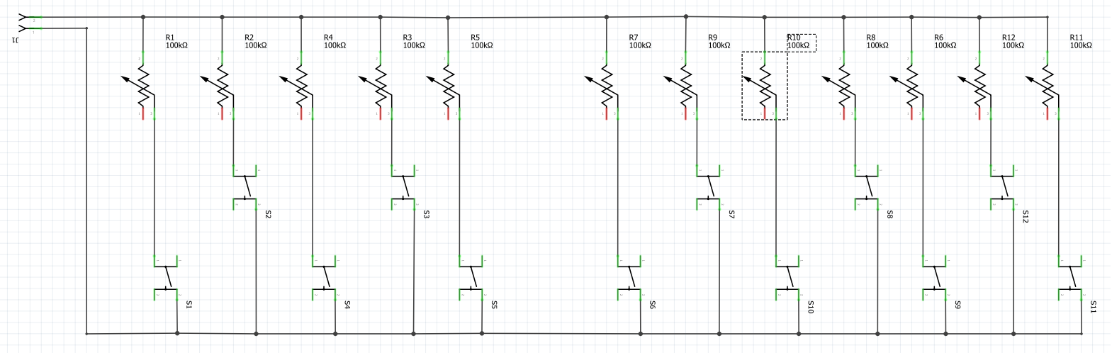
To get some sound out of this thing i need a keyboard. The schematic is basically a bunch of resistors in parallel which can be selected by the puch of a button.
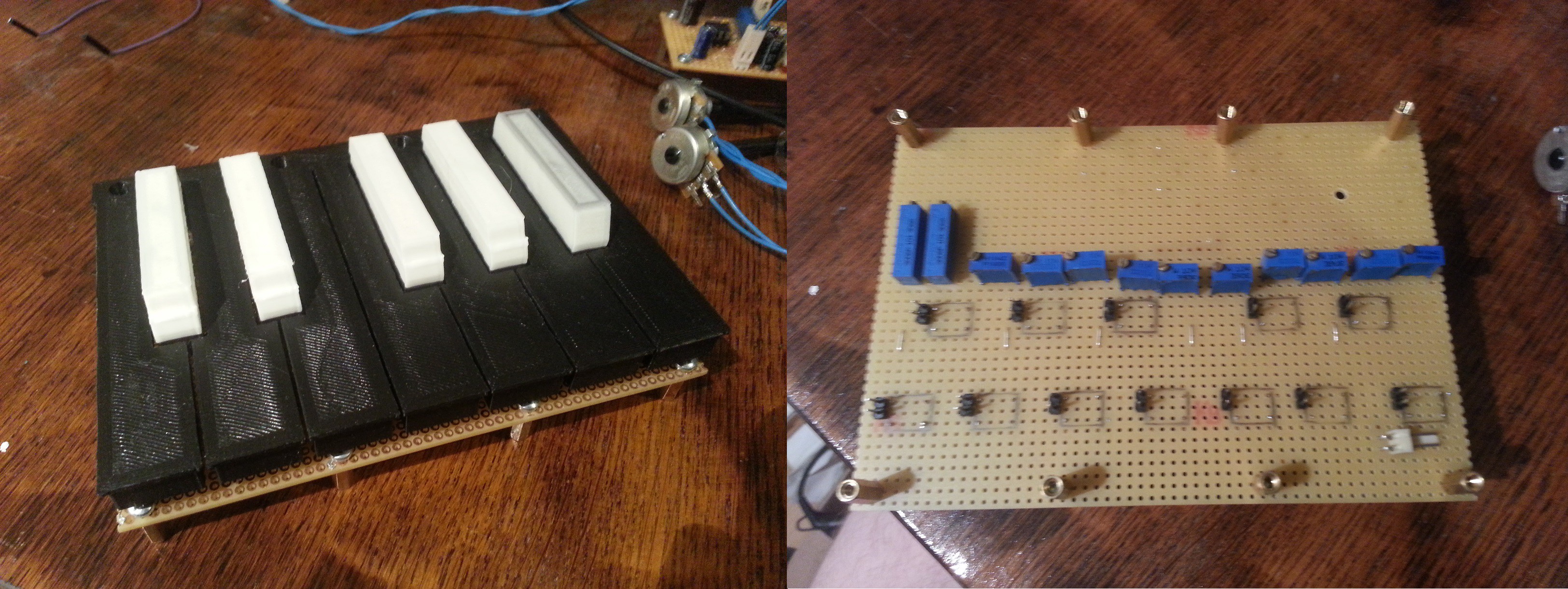
So i built a keyboard out of tact switches...... ok calm down. I know this is normally a bad thing. But in my case i put some levers in form of a keyboard over it. It still feels like tact switches. But you can hit a key without looking and feel your way around the keyboard, which i think is the feature most missed on normal tact switch keyboards. The result is actually quite nice to play.The levers are 3D printed in one piece and mounted on a pcb over the switches. The half tone keys are printed separately and cliped on the levers. The resistors are potentiometers so i can trim each tone. Each switch can be shorted by a jumper. So when i trim the tone, i don't have to press the key down and have my hands free.
This is just one octave, but you can add additional octaves. The 3D printed parts fit seamless together. And all switches are simply connected in parallel. There is no limitation to the length, except money (neither sense nore usefullness or the human listening capability)
You can find the .stl files and a board layout in the project files if you want to build your own.
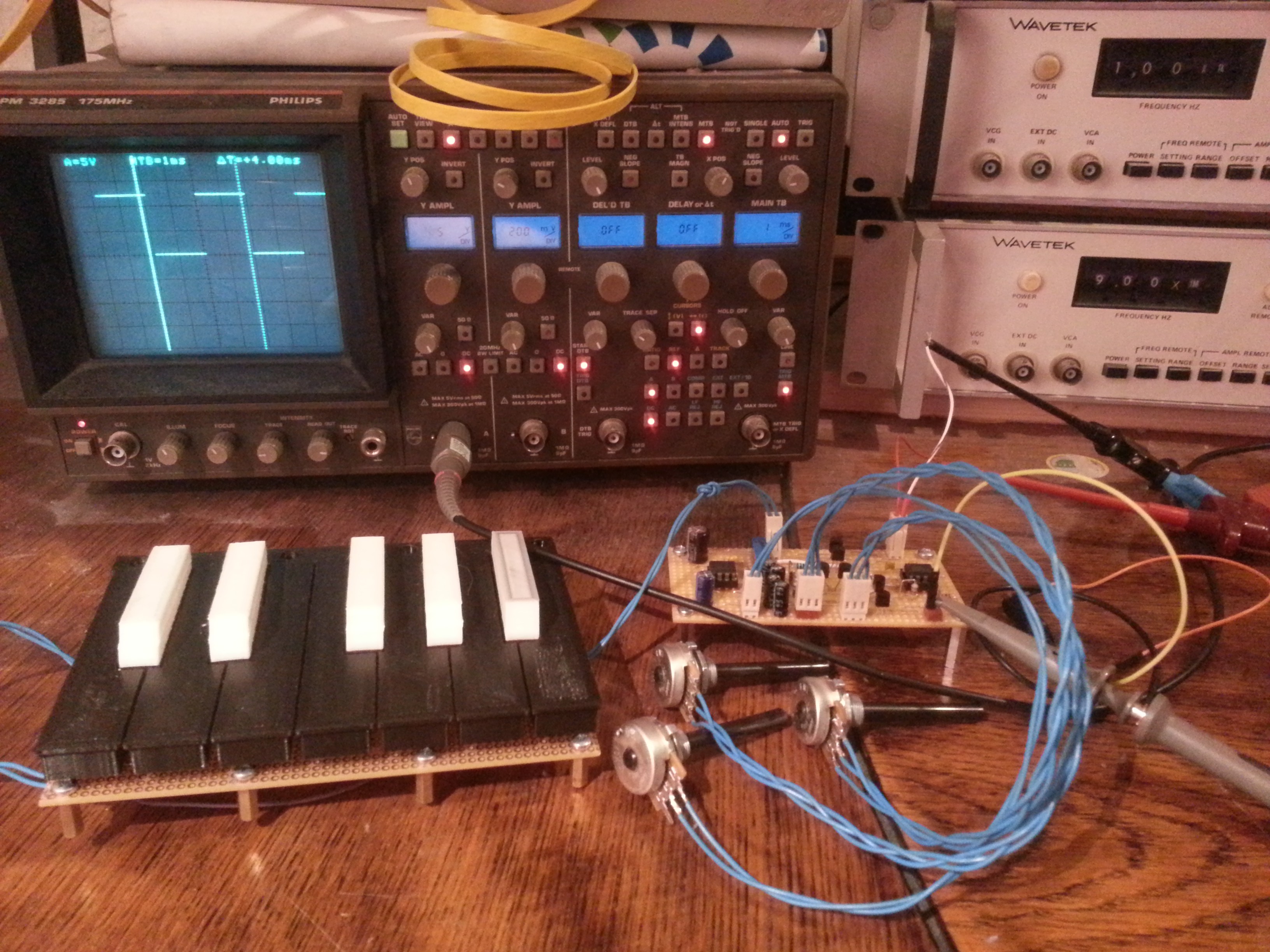
Testing the Main Voice Oscillator
I connected everything and tested the circuit. It worked on first try, no debugging required. No build errors and the function was confirmed by simulation. As a small demo you can see the rectangular wave on the scope. Frequency modulation works as well.
Unfortunately now i have to trim the keyboard. For that i need a frquency counter. I could do it with the scope, but it's not the best tool when you need an precise measurement. Besides that i have a frequency counter but it is broken, because of cause it is. So i probably fix that first.
-
VCA & Testbench
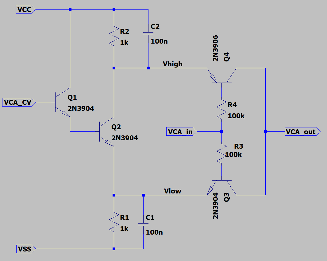
01/02/2022 at 17:56 • 0 commentsThe voltage controlled amplifier (VCA) multiplies the signal from the main voice oscillator with the signal of a second LFO. Unfortunatly this circuit violates my second rule and does not contain any NE555's. But the second LFO will contain an NE555, so we are technically clear.
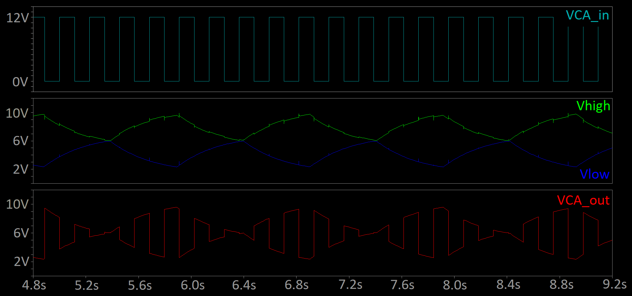
The signal from the main voice oscillator is applied at VCA_in. Q2 and Q3 work as switches. If VCA_in is at 0V (low) Q3 is turned on, Q2 is turned off and the output VCA_out is pulled up to Vhigh. Vise versa if VCA_in is at 12V Q2 is turned on, Q3 is turned off and VCA_out is pulled low to Vlow.So the signal from the main voice oscillator switches between Vhigh and Vlow. This is why the VCA only works for rectangular waveformes.
The signal from the LFO is applied at VCA_CV. Q1 and R1 work as a voltage follower. So Vlow is roughly at the same voltage as VCA_CV.
The current through R1 depends on the voltage applied to it. Therefore the current through R1 changes with VCA_CV. The same current flows through R2 which is at the same value as R1. Therefore R2 experiences the same voltage drop as R1. So Vhigh is Vlow but inverted.
C1, C2 and C3 remove some switching noise and are maybe not necessary, but my simulations look so much nicer with them.
A typical signal trace looks like this:
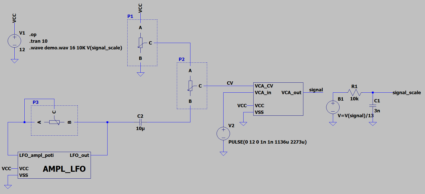
This is the testbench for the VCA:
The frequency of the LFO is set by P3. It can be set between 1Hz and 20Hz. But maybe i will update that in a future revision.
P1 is used to set the dc level for VCA_CV. It will only be trimmed once, the user will have no access to it. P2 sets the amplitude of the LFO signal and controls how much modulation is applied. B1, R1 and C1 reduce the amplitude of the output signal of the VCA, so it can be exported as a .wave file.
All simulation files and a sound demo of the VCA are available in the project files.
-
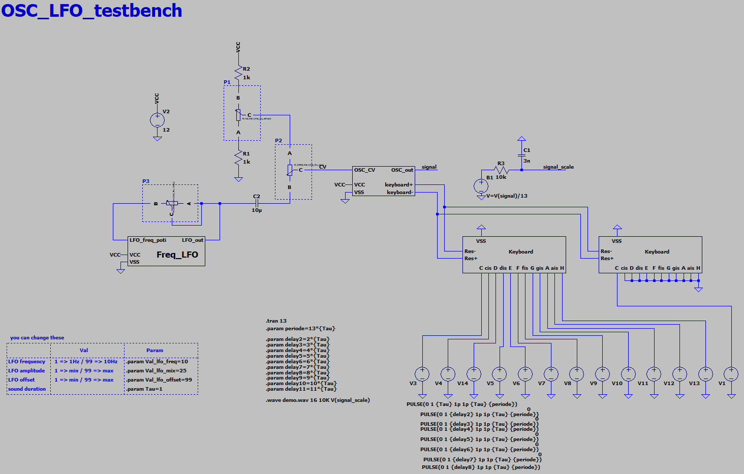
Testbench and first Noise
12/29/2021 at 02:21 • 0 commentsThis update shows the final state of the testbench i used to test the main voice oscillator and the LFO.
There ...
The block in the middle is the main voice oscillator. The LFO supplies the main voice oscillator via a Bias Tee with the control voltage for the frequency modulation. The voltage divider R1, R2 and P1 set a dc control voltage between 4V and 8V. The signal from the LFO couple through C2 and is superimposed on the dc control voltage. The amplitude of the ac part can be set by the poti P2.
Because the output of the LFO and the voltage divider are in the single kOhm range and P2 is at a 100kOhm no buffer or voltage follower is needed.The two blocks on the right simulate the keyboard. They connect and disconnect resistors depending on the inputs C to H. Each block contains one octave.
B1 is a voltage controlled voltage source and just decreases the main voice oscillator's signal by a factor of 13 because the export to a .wave file only works for signals between +1V and -1V.
You can find all simulation files in the folder OSC_II_tb.zip. After simulation you can find demo.wave in the simulation folder and can listen to the synteziser. You can change the LFO settings in the box in the lower left corner.
-
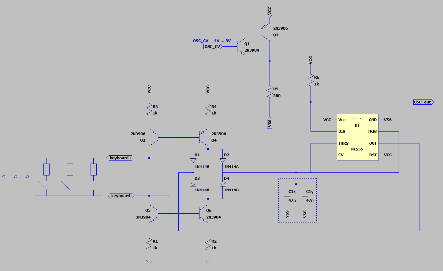
Main Voice Oscillator II
12/20/2021 at 02:25 • 0 commentsOk, the title already gives it away. I put together a testbench in LTSpice, threw in the main voice oscillator and LFO and it sounded like .... . Well, it was bad. So i had to update the main voice oscillator. I will not even put the old version in the project files.
The problem: As a standalone oscillator the circuit presented in my first log works fine. However when i tried to modulate the frequency via the control voltage (again as described below) the duty cycle of the rectangulare wave changed.
Without modulation the voltage at C1 changes between 4V and 8V. This is in the middle between the supply voltages. C1 is charged and discharged over a resitor in the keyboard. The pin OUT applies the positiv or the negativ supply voltage to charge C1. When the control voltage CV is lowered i.e. to 6V, the voltage at C1 changes between 3V and 6V. This is no longer in the middle of the supply voltages. When charged, the voltage drop above the keyboard is bigger than when it is discharged. Therefore C1 charges faster than it is discharged. The duty cycle is no longer 50-50.
I expected that and actualy thought that would make for a more "synthesizer like" sound. But it makes every key sound like it is off. It never sounds quite right.
This shows that just a transient simulation is not sufficient enought to judge a synthesizer design. Exporting the simulation results as a .wave file saved me time and a useless prototype.
The Fix: The duty cycle needs to be independent of the control voltage CV. The best way to do this is to set charge and discharge current of C1 by constant current sources and just switch between them instead of charging C1 directly from the NE555.
I came up with this circuit. Unfortunatly it violates my thired rule (as simple as possible). Sue me!
The charging current of C1 is provided by the current mirror Q3, Q4 ,R3 and R4. Discharge current is provided by Q5 ,Q6 ,R1 and R2. When the pin OUT of the NE555 is at 12V the diode D1 does not conduct (the anode of D1 would have to be at least 12.7V). The voltage on C1 is between 8V and 4V, assuming the control voltage CV is not modified. So D2 conducts and the charge current flows to C1. Diode D3 is conducting. The cathode of D3 is pulled up to 11.3V. So D4 is reverse biased and does not conduct. No discharge current can flow from C1.When the voltage at C1 reaches 8V the pin OUT changes to 0V. Now the anode of D1 is pulled down to 0.7V therefore D2 is now reverse biased. D3 does not conduct and the discharge current flows from C1 through D4.
To change the key of the synthesizer the charge and discharge current have to change depending on the key pressed.
When a key is pressed current flows through R3 and Q3 and provieds the bias for the chargw current source. It goes through the keyboard and through Q5 and R1 and provides the same bias to the discharge current source.
The voltage across Q3 and Q5 is assumed to be constant at 0.7V. The rest of the supply voltage of 10.6V drops off over the resistor of the keyboard and sets the charge and discharge current. The keyboard resistors are in the range of 20kOhm to 80kOhm. R3 and R1 are small and can be neglected.
When no key is pressed there is no current flow through the current mirrors and charge and discharge current are zero, the main voice oscillator stops.
Frequency modulation works the same way as for the main voice oscillator version I.
-
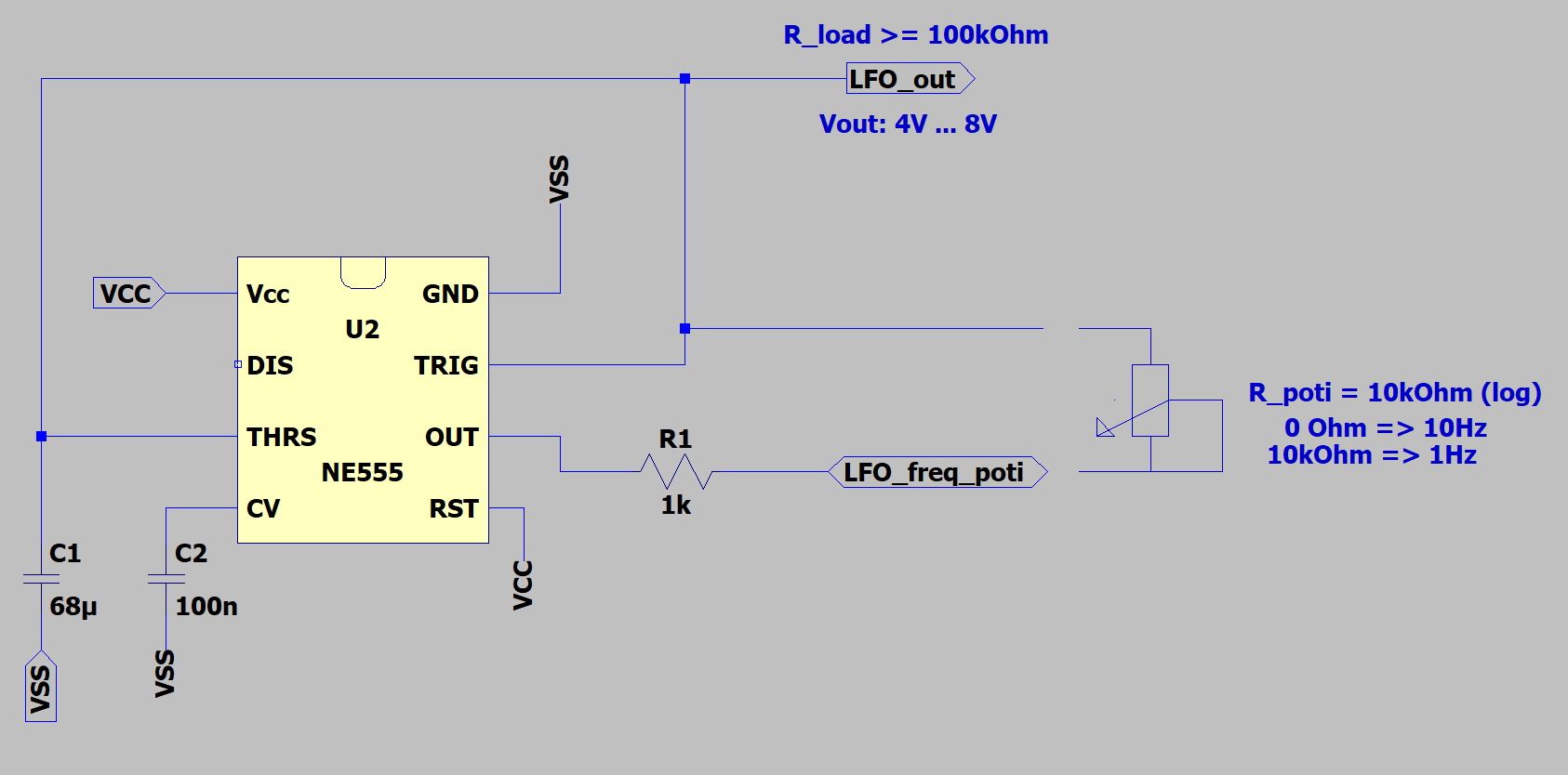
LFO I
12/12/2021 at 02:40 • 0 commentsLFO I will be used to modulate the frequency of the main voice oscillator.
The operating principle is pretty much the same as for the main voice oscillator. Capacitor C1 is charged through R1 up to 8V. This triggers the NE555 to set the pin OUT to 0V and C1 is discharged down to 4V. the NE555 sets pin OUT to 12V and the cycle repeats.
The charging and discharging creates a sort of triangular signal voltage over C1. This will be used to modulate the main voice oscillator and generate continuous frequency sweeps.
To not interfere with the charging and discharging cycle, the resistive load put at LFO_out must be significantly higher than R1 and the poti. The load resistance should be at least 10x bigger.
C2 is just buffering the internal voltage divider of the NE555, nothing fancy here.