-
Reusing the idea
12/14/2022 at 00:37 • 0 comments![]()
The circuit design for the nixie drive transistors in this ancient piece of equipment has been reused in my #Modularnixie project taking advantage of modern PCB manufacturing and assembly.
-
Final touches
04/13/2022 at 06:29 • 0 comments![]()
The deficient digits did heal with use, especially the ten hour digit so I have no more excuse to sleep in after 1000. 🤣
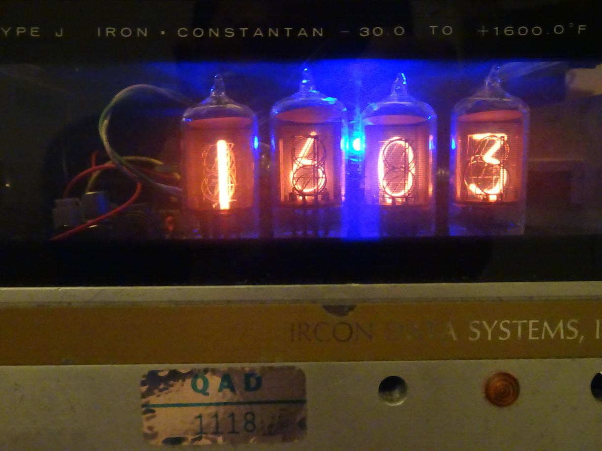
It's common to surround nixies with a complementary colour of light such as blue, Due to the socket and tube base, it's not possible to do this through the bottom. So I tried placing a couple of LEDs in the background. Unfortunately the back of the nixie is opaque to prevent the glow from lighting the back or sides so the photo is the best I could do. 🤷
-
Closing the case
04/04/2022 at 07:10 • 0 comments![]()
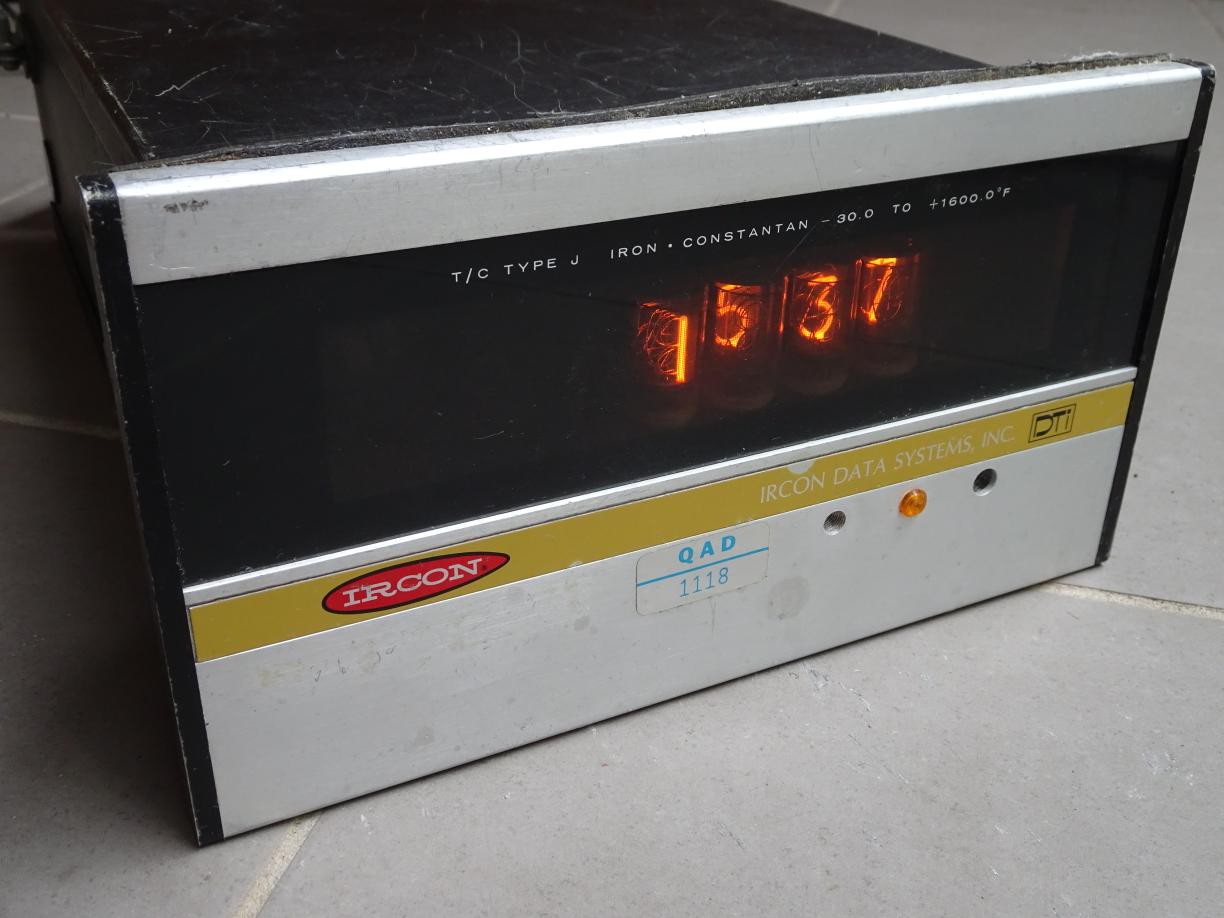
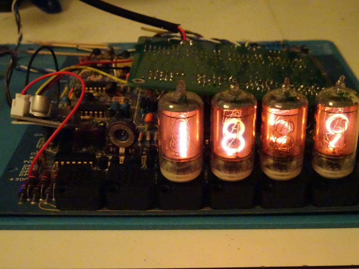
After the board had been running smoke-free 😉 for a while I cranked up the HT to 200V and the nixies brightened up. One of the 5 nixies turned out to be dead (gas leaked out?) so I have no spare if any of the 4 fail. Perhaps I could plug the symbol nixie into the 10 hours position for a weird display, which is acceptable as my other clocks are weird too. 🤣
In the photo you see a drawback of nixies, i.e. the digits are not in the same plane; the 5 is noticeably further back than the 1 in front. So nixies need to be viewed face on.
Another thing I noticed was some digits were not fully-formed, part of the cathode wouldn't glow. Still readable though. I swapped the nixies around so that the deficient ones would be in less important positions. I put the nixie with a deficient 8 in the 10 minute position which will never show 6-9. I put the nixie with the deficient 0 in the 10 hours position. In this workaround I sleep in until after 10 so that I don't see the 0. 🤣
A bit of searching for information about nixie wear found a post where it was suggested that nixies that have been out of action for a long time need to be "exercised" and the cathodes will heal. I hope that is the case. I won't try those remedies that suggest overdriving the nixie for a while. In my spare time I might research deeper out of curiosity. Anyway there is nothing I can do, short of paying too much for replacements. They work as well as I can expect. I just wish the case wasn't so big.
![]()
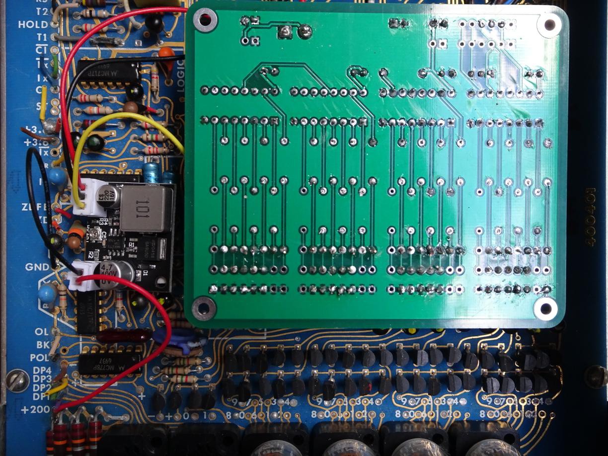
Here you see the two extra boards added to the main board. On the left is the matchbox size 12V to 200V boost converter and the larger board is the #3 line to 32 line output expander. Hmm, I should clean it up a bit with isopropanol. The main board is now just a carrier for nixies, the rest of the circuitry on it is not connected, save through GND, and not powered. 12V from a standard SMPS adaptor powers the unit, and the MCU board is at the back of the case so that the set buttons are accessible.
So that's it then, I can have my bench space back. Closing the case now. 🤣
-
Light up!
04/01/2022 at 08:47 • 0 comments![]()
After the previous log, I wired up the outputs of the expander to the identified points on the base PCB with 28 hookup wires, plus 1 ground wire. Fortunately I had enough wire in many colours so I could colour code the lines.
Next I connected the 200V anode line on the board to the 12V power supply. A couple of blue and white LEDs were plugged in with the cathode lead to the 0 and 1 cathode holes and the anode leads to the anode hole of the tube socket. With about 9V across the 20k resistor this gives about 0.45 mA current, enough to light the LEDs. The LEDs duly turned on when the minutes ended in 0 or 1, proving that the biquinary drive scheme was working properly.
I left it like that for a week as I had other life matters demanding my attention, and also to allow any possible issues to emerge.
Tonight, tired of procrastination and cowardice, I disconnected the 12V jumper then wired up the 12V to HT boost module and the HT out to the anode supply point. With no nixies plugged in, I measured the HT at about 170V. Must have been set at that by the factory. I cranked up the HT line with the trimpot to about 175V to ensure reliable firing. Later on I'll raise the HT to the rated 200V for full brighness.
I plugged the nixies in and they just worked. Must have been decades since the gas inside was ionised. The minutes digit had a bug where it simultaneously showed both 4 and 6, or 5 and 7. This was simply the result of solder bridge between the 4/5 and 6/7 drive lines and readily fixed.
The result is in the headline photo. I'm chuffed. 🤗 And no, it's not a joke, I know what day today is. Good start to the weekend.
-
Preparing the nixie board
03/15/2022 at 05:44 • 0 comments![]()
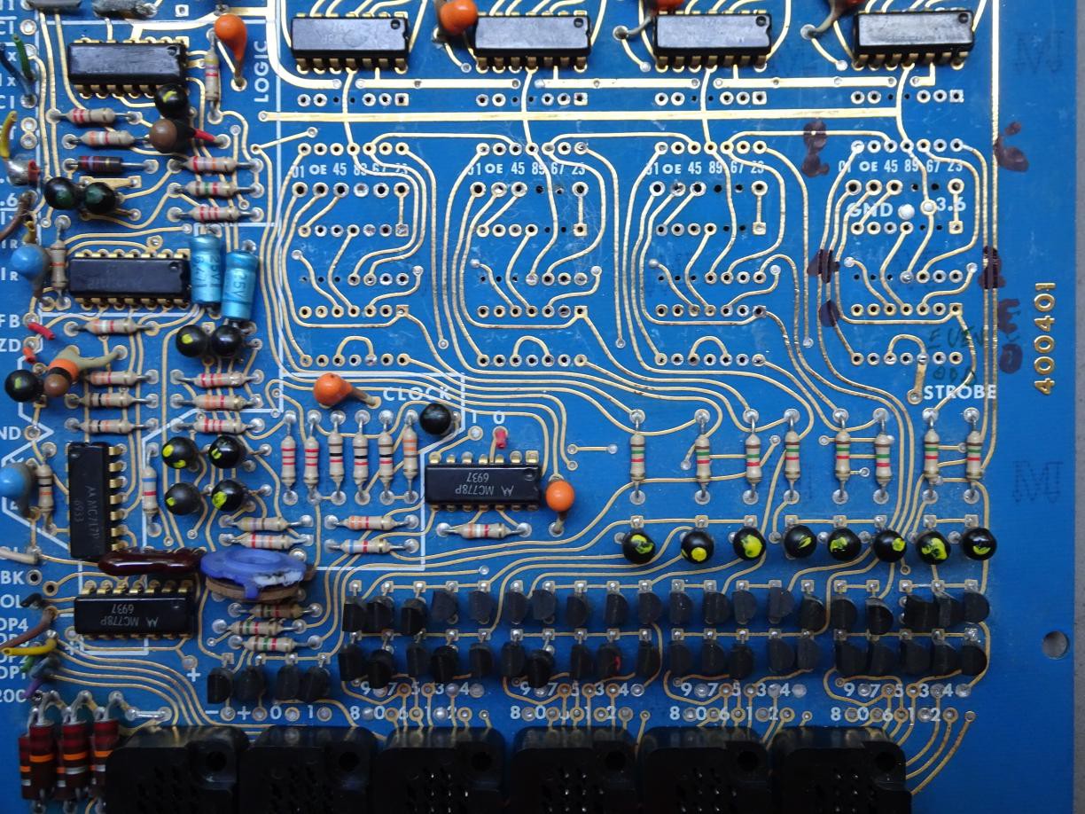
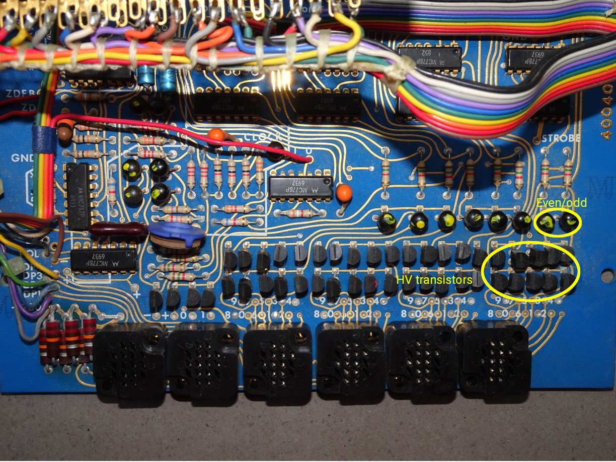
As mentioned in the log Decoding the decoders, a biquinary scheme is used to drive the cathodes. Briefly, there are 10 HV switching transistors, but they are arranged in 2 banks of 5, with a low side transistor switch to select the odd or even bank. This means that 7 lines are used to select 1 of 10. You can see the 4 banks of 10 above the sockets, and the 4 pairs of bank selector transistors above them. These were driven from the flip-flops. I will be driving them from my #3 line to 32 line output expander board.
I removed the flip-flops so there are no stray connections to the bases of the transistors. Even though the old RTL logic remaining on the board will not be powered, there might be stray paths to ground. Desoldering the flip-flop ICs wasn't as difficult as I feared. I needed only a normal conical tip soldering iron and a vacuum solder sucker. I didn't want to escalate to the heat gun because that can damage the board and components. In the end 10 out of the 12 ICs came out undamaged and I broke 2. After that I gave the area a good wipe with isopropanol.
Notice that some of the pads were lost. Those didn't survive the heat. This double sided board doesn't have plated through holes, either the trace was on one side only, or the component lead passed the connection through. I think in that era PTHs were done using rivets. But since the pads I want are terminating connections, I only have to solder my wire on the side with the pad and trace. I identified the correct pads by tracing to the bases of the transistors, and labelled them, but I didn't have a fine tipped marker. No matter, I've documented the layout on paper. The layout is identical for all the other digits.
If you have a sharp eye you'll notice some wire pads labelled 01 OE 45 and so forth. These are in fact the inverse outputs from the flip-flops (i.e. the ~Q outputs) intended to drive the comms board, no longer needed, so not relevant to my scheme, but helpful to confirm the correct pads.
-
Testing the addon boards
03/06/2022 at 07:15 • 0 comments![]()
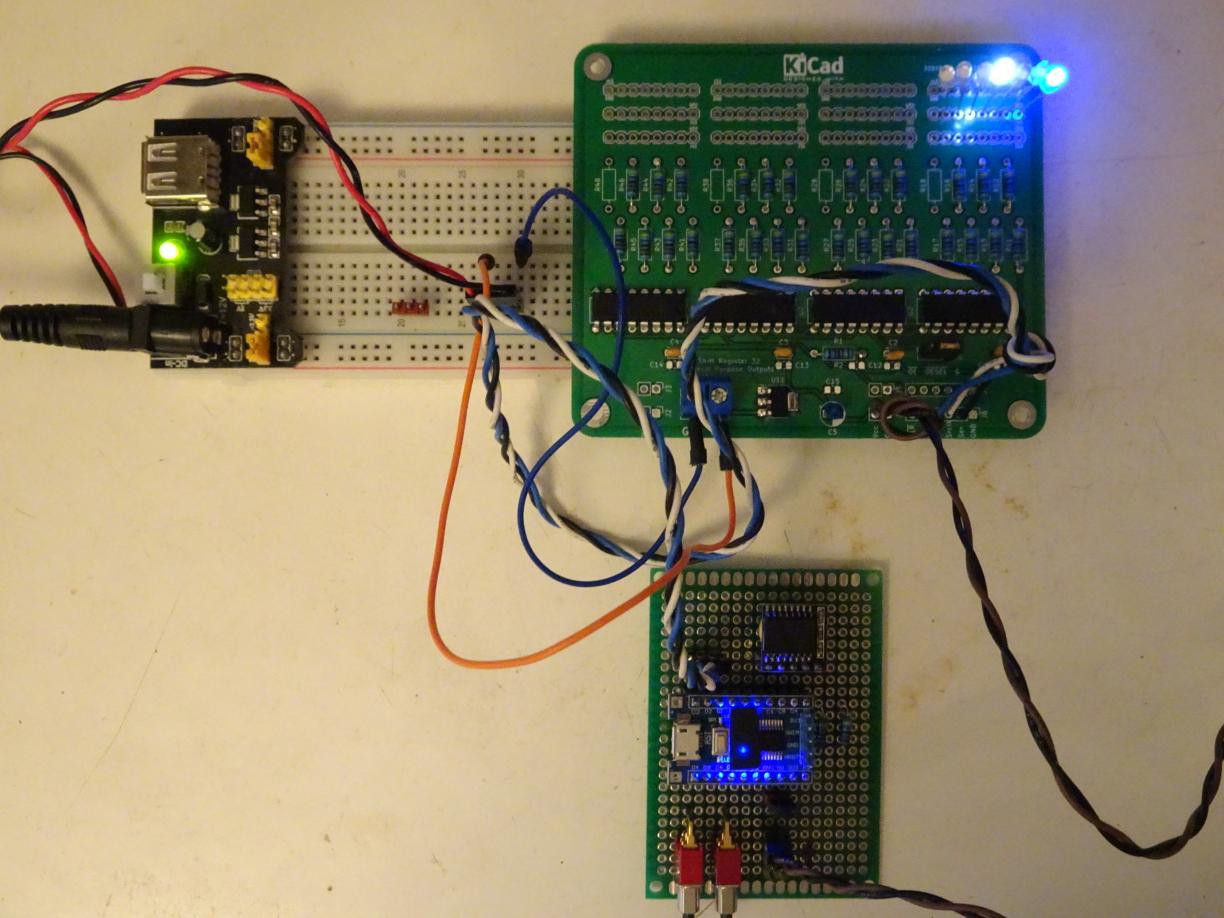
Least significant nixie digit drive shows Even and 2/3 lines active, thus the 2 cathode is to be on.
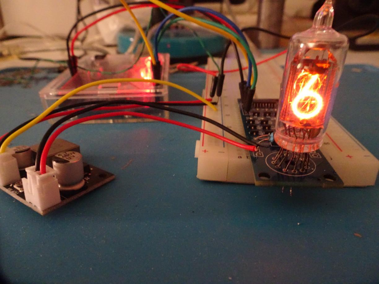
Now that I have assembled the #3 line to 32 line output expander board, there is no more excuse for procrastination. So I connected it up to the #Quick and simple STM8 board with TCXO, rebuilt the software to drive the 74HC595 shift registers instead of a TM1637 and flashed the STM8 MCU. Since the DS3231 TCXO keeps time even in the absence of power, I know what to expect the display to show. I have connected LEDs only to the least significant digit (minutes) but from previous testing, the whole shift register chain should work.
At the top left is the power adaptor board which regulates the input voltage from a 12V wall wart power supply via the barrel socket to 5V and 3.3V. Here it's used only to tap into the 12V as there is a 5V LD1117 regulator on board. The adaptor is a dollar or two ordered online. The board is plugged into a breadboard which here only provides connection points. It was previously used with the Arduino Uno for earlier testing.
The third board, not shown, is an off-the-shelf 12V to 200V (adjustable) boost converter. All of the add-on boards to the thermometer will be powered by the 12V wall wart. The expected draw from the power supply is around 200-300 mA, well within the capability of the many spare wall warts in my spares hoard.
-
Preparing new circuitry
02/22/2022 at 10:06 • 0 comments![]()
There have been no posts but I have been designing the replacement circuitry for this ancient box. The shift register PCB will be delivered soon. Originally I thought I would use an ESP8266 or ESP32 module to read data to display over WiFi. On further thought there isn't much you can send over the air to numeric nixies so it would be a waste of technology. Instead I will connect a STM8 based clock board using a DS3231 TCXO for accurate timekeeping, briefly described in #Quick and simple STM8 board with TCXO.
So there will be three small boards to put into the case, the clock board, the shift register board, and an off the shelf 12V to 170V boost converter. The whole thing can be powered by a 12V wall wart.
The picture above shows the clock board being tested with a TM1637 display.
-
Interface design
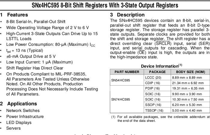
01/08/2022 at 09:52 • 0 commentsI already have an idea of what the shift register GPIO should look like. In a previous project #An uninnovative linear LED display I put the 74HC595 8-bit serial in parallel out shift register to work. This is a remarkably useful and cheap chip. It contains a latch so that the data shifted in can be held until the next update. It can be cascaded to any practical length. It can source or sink current. It's is very simple to drive, the software routine is easy to understand.
![]()
4 digits means 28 lines are needed. The next multiple is 32 = 4 shift registers, so I can allocate a whole byte to each digit. The length of register chain is not a problem as it doesn't take long to shift in 32 bits, much shorter than the update period for the envisaged use as a display.
While I only need one interface for this project, the horrors of perfboard assembly have put me off anything more complicated than a chip or two. 100x100 mm PCBs are so cheap, only a couple of bucks each delivered, so I will make a design that I can reuse for other projects. It will be a general purpose 32 line GPIO, or rather GPO, board.
This project will go into hibernation until I have finished the SRGPO project.
-
Driving the nixies with extra circuitry
01/06/2022 at 23:37 • 0 commentsAlthough I have suggested that the counters may be arranged in a 1-2-2'-4 configuration rather than 1-2-4-8, this has not been verified by more circuit tracing. But I don't have to do this because I don't intend to use the counters anyway.
So the question is where to interpose an extra circuit to drive the nixies from a WiFi MCU, as planned? Should it be before the latches, or after? After is easier, as the shift register GPIO will already come with a latch, and there is no need to power the MC778s to keep them working as latches. Instead of cutting traces, probably the easiest way to connect to the driver transistors is to desolder the MC778s from the board, using some combination of soldering iron, solder sucker, solder wick and heat gun. This also has the advantage that the pin holes exposed by the removal of the chips are concentrated in particular areas corresponding to the digits, so the flying leads to an auxiliary PCB will be neater.
As mentioned the driver scheme uses 6 inputs to encode 0-9. The even/odd input is actually 2 lines, so 7 lines are required in all. We could invert the even input to get the odd input, but a shift register GPIO will have lines to spare so we can avoid an inverter.
There is actually one more pass transistor below the even/odd transistors, which seems to be for display blanking. Easiest solution would be to simply bridge the C-E pins of that.
I haven't discussed what to do with the symbol nixie and the 0/1 nixie. At this point, the easiest solution is to just unplug those nixies, to get a 4 digit display, one spare digit nixie, and one symbol nixie to ponder what to do with.
Another goal was to substitute a more efficient power supply. Since the RTL chips don't have to be powered as the driver transistors only need base drive current, I no longer need the 3.6V logic supply. The 200V nixie supply can be replaced by a boost converter. Then I don't need to supply any power to the transformer and all the other circuits on the board won't draw current. The whole box and the WiFi MCU could be powered by a wall wart SMPS. That also solves the problem of the dangerous exposed mains terminals at the back. I could remove the RS232 socket to provide an entry hole for the interface cable.
My ideas on the shift register interface and the power supply will be in the next log.
-
Decoding the decoders
01/06/2022 at 10:18 • 0 commentsNow I have to work out how the nixies, which are 1 of 10 indicators (ignoring the decimal point) are driven from binary inputs. So I examined the driver transistors and the display latches feeding them using optical trace scanning (my eyes 😉) and a continuity meter.
![]()
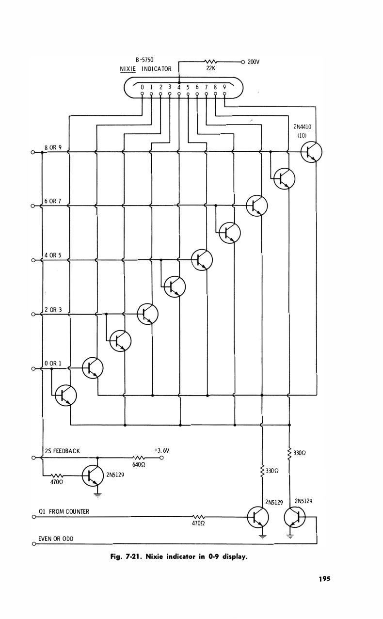
Each nixie is driven by 10 transistors grouped 5x2. Each pair of 5 pairs has bases wired together. The reason will be evident in a moment. The circuit is pretty much similar to the following page I have excerpted from the RTL Cookbook I fetched. So instead of 4 binary inputs weighted 1-2-4-8 as we would expect nowadays, there are 6 inputs. The first is the even/odd line, and the others are the 0/1 2/3 4/5 6/7 and 8/9 inputs. So for example to display a 7, the odd input is active and the 6/7 transistors are driven but only one will conduct, the one whose emitter is grounded by the odd driver transistor.
![]()
Tracing the inputs of the transistors from the MC778 chips reveals that two 2N5134 transistors switching between even and odd digits are driven in antiphase from one flip-flop using the Q and ~Q outputs. The 5 other flip-flops drive the 5 pairs of 2N4409 high voltage transistors. These 6 flip-flops contained in 3 MC778 chips, and there are 4 columns of 3, for the rightmost 4 digits. We'll ignore the leading 0/1 and the +/- nixies for now.
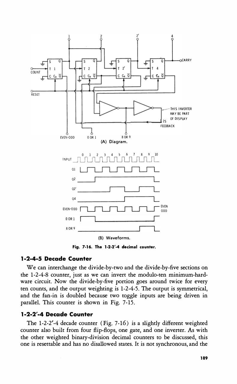
How does one get from a BCD counter to this biquinary code? The RTL Cookbook provides one answer. The counter stage is not a 1-2-4-8 scheme, that requires too much decoding. Instead it is probably a 1-2-2'-4 scheme shown in the next diagram. By the use of a few extra gates this is converted to a biquinary code. So the "comms board" I showed earlier is most likely a code converter board. It contains multiple MC717 NOR gates and the wiring loom goes to the main board near the flip-flops discussed.
![]()
There is another small mystery. There is no current limiting resistor on the bases of the 2N4409 HV transistors. This means that the design is relying on the collector pullup resistor of the RTL flip-flop to limit the current. The nominal value given in the datasheet is 3.6k. With a voltage supply of 3.6V and a B-E drop of 0.6V, this means a bit less than 1mA current drives the HV transistors. That is plausible. But there is another question: doesn't this load down the high level of the flip-flop so that it's not a true 1? Yes it does, but as the flip-flops are used as buffer latches and the outputs don't drive other RTL logic gates, this has no consequences. Obviously the designer did this deliberately and saved quite a few resistors this way. 👍
 Ken Yap