Jesse Farrell
-
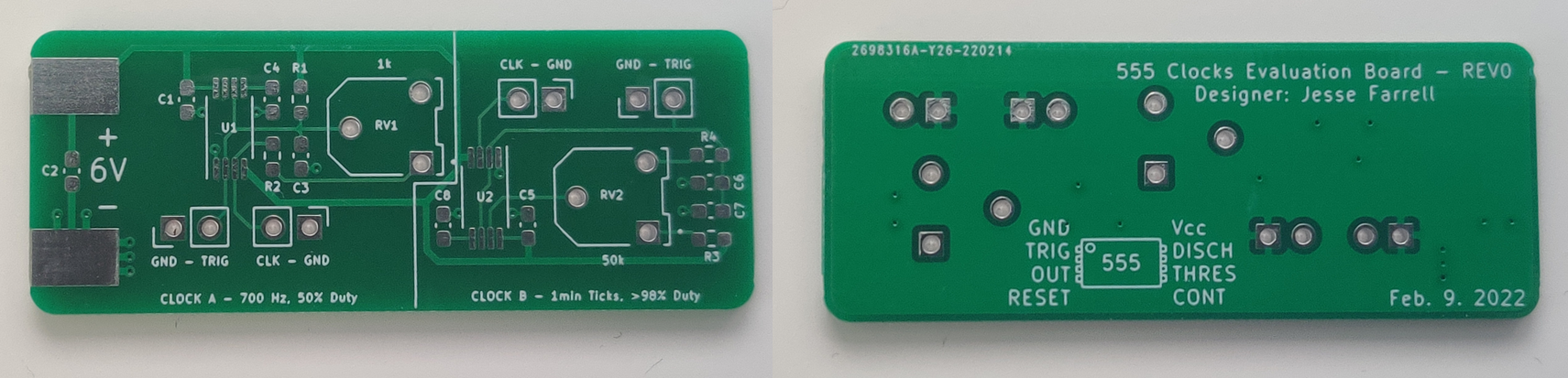
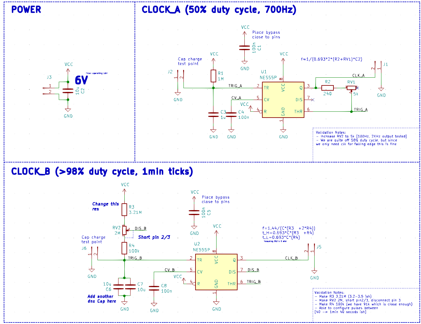
Validation – Clock A/B Sources
03/05/2022 at 18:30 • 0 commentsThe validation Circuit schematic and pcb are shown below. There was one mistake in Clock_B’s circuit; RV2 needs to have pin 3/2 shorted, this allows us to tweak the frequency instead of just the duty cycle of the output. Other then this there were a few component value changes to allow me to hit the desired frequency in both circuits (neither circuit followed their formula particularly well).
![]()
![]()
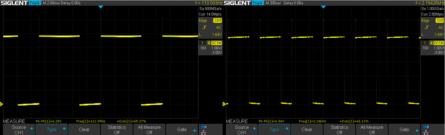
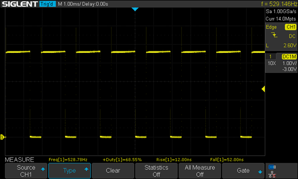
Here are some of the captures for the clock sources. Clock A can be configured between 100Hz to 2.2KHz when using a 5k potentiometer.
![]()
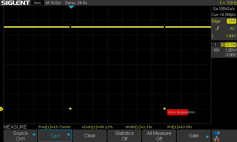
Clock B can be configured for a 45seconds to 1min 30 second period. Note the short -width is intentional.
![]()
-
Eval Boards
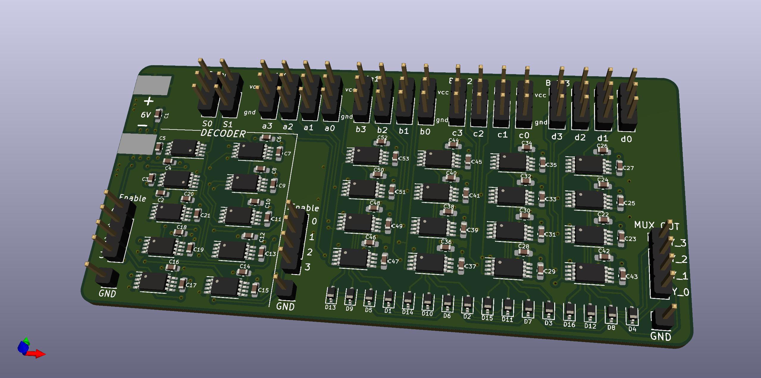
02/06/2022 at 22:39 • 0 commentsI’ve done layout for 4/7 evaluation boards of the widget. There all two-layer boards with a ground pour on the bottom layer. Each boards costs about $2.50 from JLC.
Here’s the 555 MUX eval board, and a timelapse of the layout if your curious - https://www.youtube.com/watch?v=jSAdDRiDnlY.
![]()
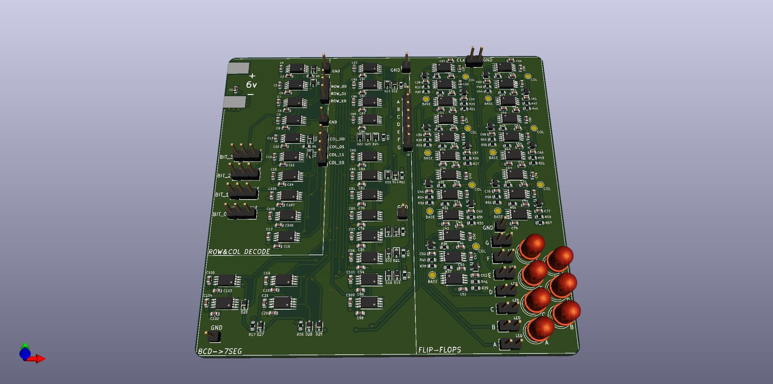
Next, I did the BCD to 7Segment Decoder, and again timelapse if your curious - https://www.youtube.com/watch?v=kENF7PsEeCI.
![]()
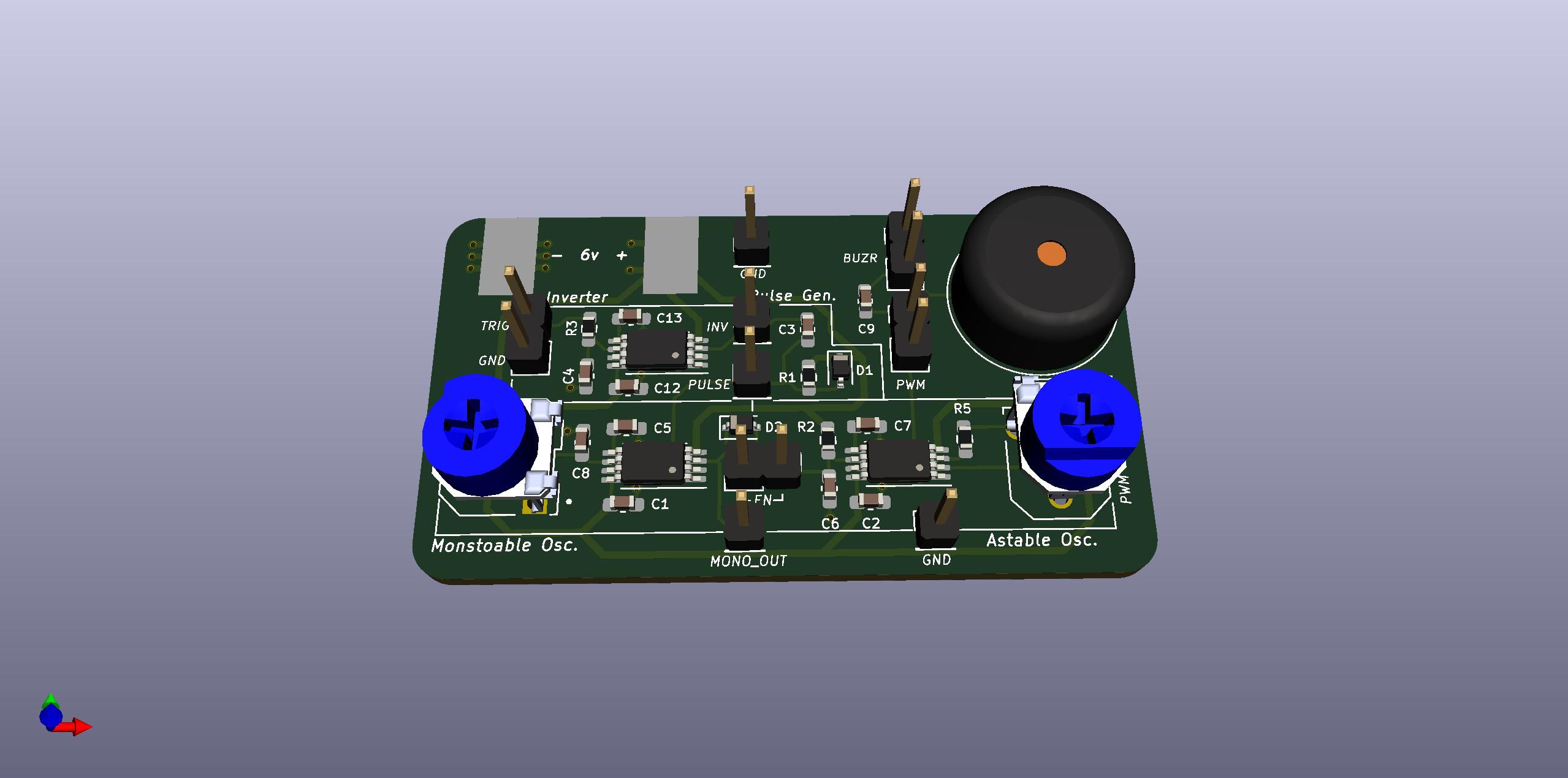
Next the buzzer circuit, which I’ve already breadboarded; but I’m on a layout blitz so I figured I might as well. Layout video - https://www.youtube.com/watch?v=HsLt1bdORC0.
![]()
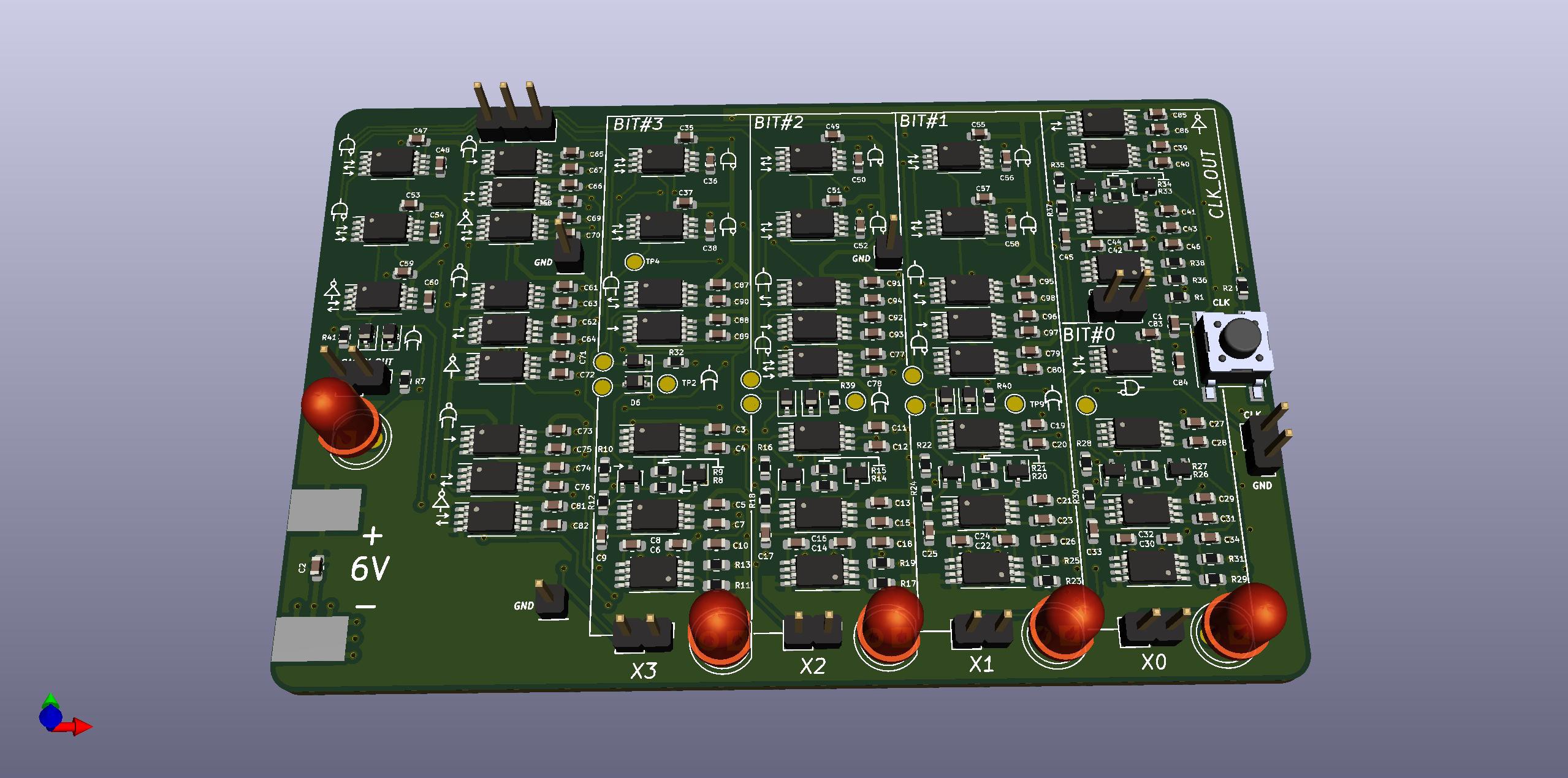
Last is the BCD counter. I should have paid more attention to the power routing of this board. Luckily there aren’t any fast/ high current signals on this board so I doubt it will cause any issue. I’ll keep an eye on it during validation nonetheless; mainly out of curiosity. Layout video - https://www.youtube.com/watch?v=oETrw1bGvMY.
![]()
-
Possibly Final Update
01/10/2022 at 16:28 • 0 commentsThought I'd post one more update before this project gets put on the backburner for awhile. Basically, I got a little carried away, and the BOM/ FAB costs reflect that. The final project would cost me about $250 for a single prototype (BOM is ~$160, FAB is ~$70, plus shipping import ect).
Future work: I'm still pretty interested in this design, so I might redesign the main board with multiple small 2-layer boards containing the different blocks. These "cards" could be plugged into a main board to help reduce the XY footprint of the design. Alternatively, I could try to populate both sides of the board; I avoided this in REV0 due to a bit of a time crunch.
Update: Well I just bought a couple hundred 555's so I guess I'll continue with this project between classes. Next step is to layout some smaller validation boards for the different blocks (MUX, BCD counter, BCD-7Seg Decoder, Flip Flop).
-
Schematic
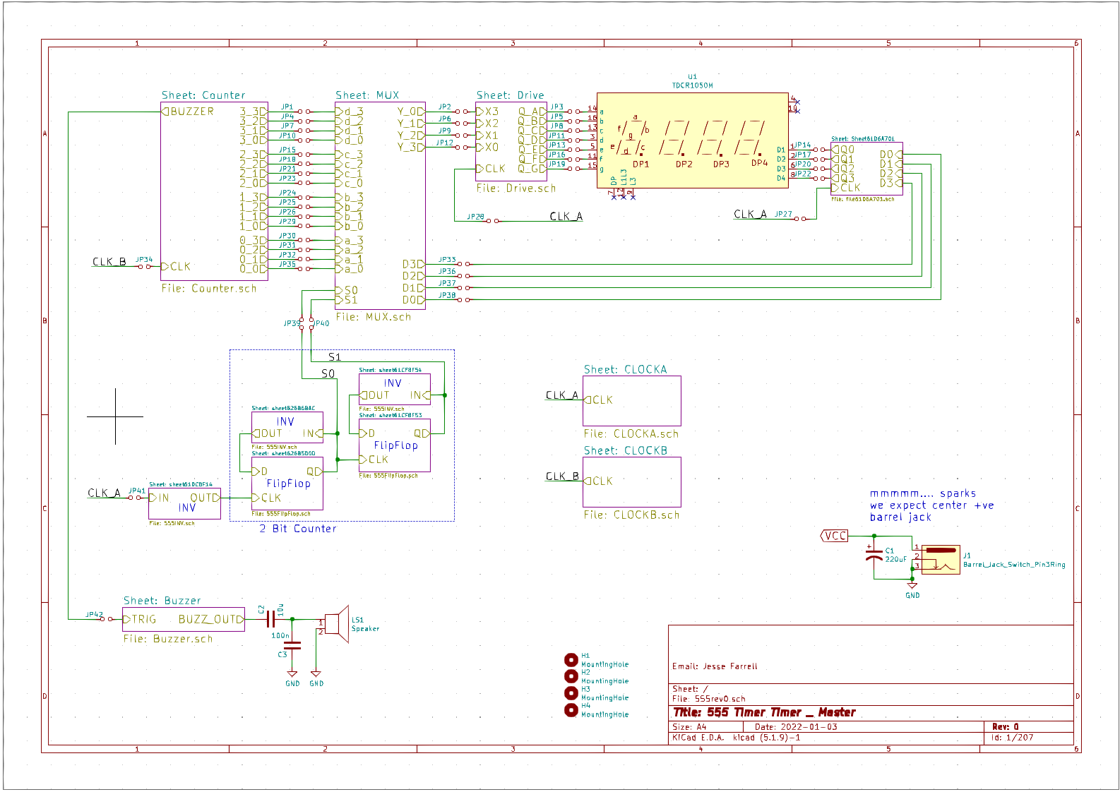
01/09/2022 at 21:16 • 0 commentsThe final schematic is shown below with all the different blocks discussed throughout these logs (for full documentation see HAS). Note that I seperated all the blocks with jumpers to simplify validation.
![]()
-
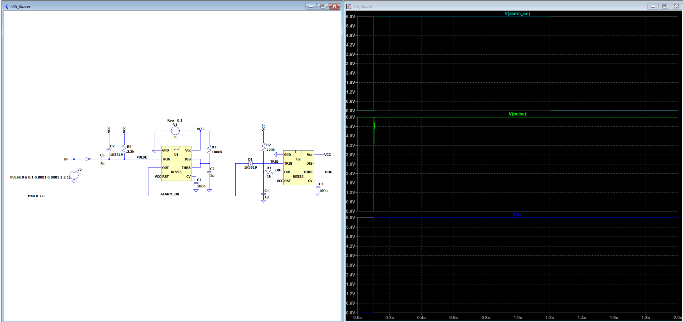
Buzzer
01/09/2022 at 21:12 • 0 commentsWhen all the bits of the counter are 0, the buzzer should start and continue for a second or so. The CLK_OUT from the last BCD counter is 0 when every bit is 0. Therefore we can trigger the BUZZER circuit with the final CLK_OUT from the counter. Note that the buzzer will artificially trigger when the user is cycling through DIGIT#3 from 0->9.
The CLK_OUT signal will then be routed to the circuit shown below.
![]()
Basically we turn the rising edge of the square wave into a pulse and use that to trigger a monostable oscillator which then enables the astable oscillator. The speaker is then driven with the output of the astable oscillator (just a square wave, no fancy waveforms here).
-
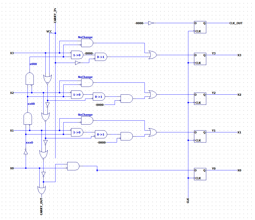
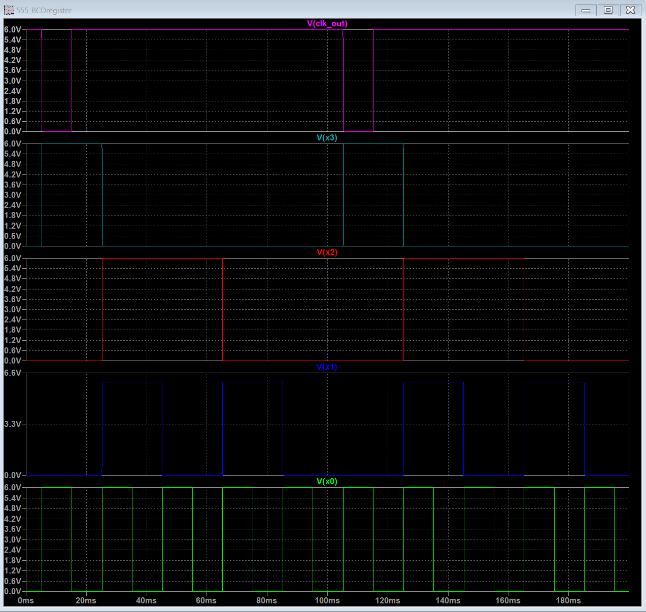
BCD Counter
01/09/2022 at 18:36 • 0 commentsThis circuit tested my sanity.
.
.
.
The counter will take clock B as an input (slow clock). With each clock pulse the contents of the counter need to be decremented by 1. There will be 4, 4 bit registers that contain the base 10 value for each seven segment digit. Meaning if the counter is displaying 2355, the registers should contain the following [0010/0011/0101/0101]. After the next clock pulse, the contents will be decremented and registers will now contain [0010/0011/0101/0100].
Having avoided for the most part neglected digital logic since second year, this circuit by far was the most difficult to configure. There’s likely some way to condense this circuit, however, due to a bit of a time crunch no further improvements will be made. The final counter circuit is shown below.
![]()
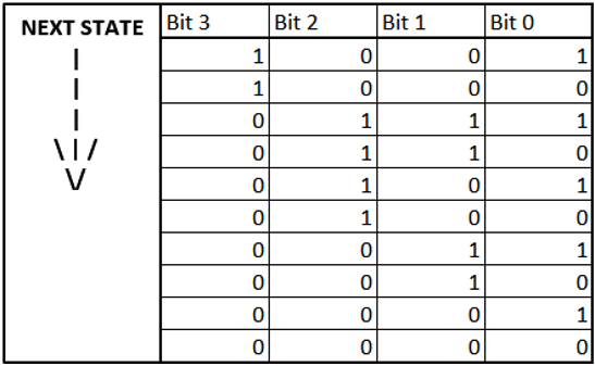
The logic for each bit is practically mirrors (excluding X0), so the logic will be explained for X3 and the reader should be able to make sense of the subsequent logic. It may be helpful to refer this table.
![]()
For a transition from 1 to 0 requires that all lower bits are 0. To transition from 0 to 1 requires that all lower bits are 0 and there is a 1 in any of the upper bits. For the highest bit X3, this is pulled from the next BCD block using CARRY_IN. Similarly, when bit X3 transitions from 0 to 1 the next BCD block is given a clock pulse via CLOCK_OUT. Note that CARRY_IN is used to set the output back to 1001 (9).
One major flaw of this circuit is that the initial state is unknown. As a result the 7SEG will display garbage until the user cycles the clock (or the clock is allowed to tick away) into a valid range (digit 0->9). Once in its valid range the counter will be locked in the range of 9->0. If a revision of this circuit is made I will address this bug (this project has already ballooned as is).
Here are the simulation results with CARRY_IN held high.
![]()
Heres a capture of several cascaded BCD counters. I've zoomed in on the 0->9 transistion to ensure that the counter loops to 1001 and not 1111.
-
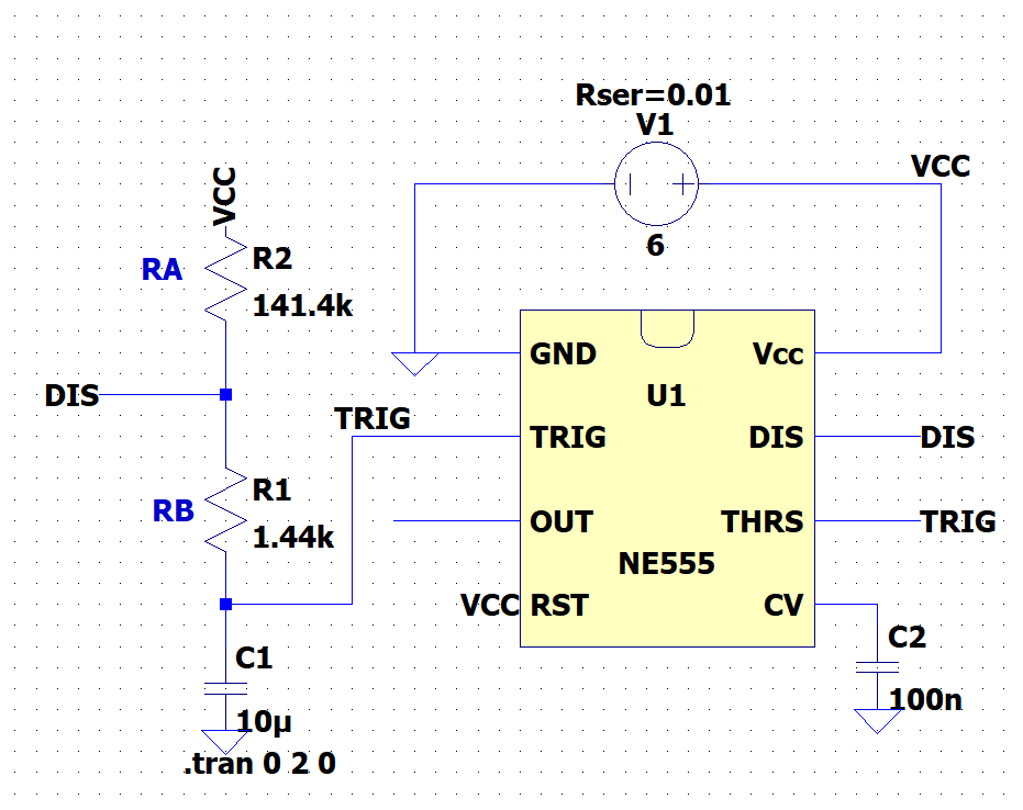
0.017Hz CLOCK
01/09/2022 at 18:23 • 0 commentsClock A will have a period of 1min, and will be used to increment the BCD counter block. Unlike Clock A, Clock B will target a very large duty cycle (short off time) using the astable multi-vibrator configuration. This allows the user to inject their own clock pulses by pulling the output low. I'll add some DNS components to the final design to allow tweaking of the charge/discharge circuit.
![]()
-
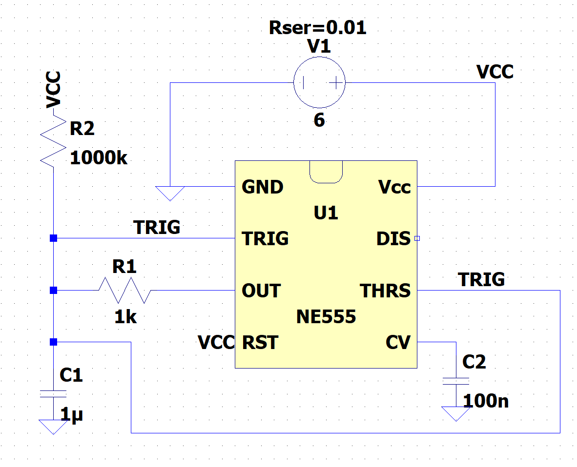
~700Hz Clock
01/09/2022 at 18:13 • 0 commentsClock A will be an astable 555 configured for 700Hz. We can achieve near 50% duty cycle using the configuration shown below. By introducing feedback between the output and C1, the capacitor charge and discharge is primarily controlled by R1. Charging will also be slightly helped out by R2, but if this value is large enough it should be negligible. [f ~ 1/(0.693*2*R1*C1) ]
![]()
And here are the breadboarded results. Not perfect but the values can be tweaked pretty easily.
![]()
-
Decoder
01/09/2022 at 18:05 • 0 commentsThis is a basic decoder that takes in a 2-bit input and toggles 1 of 4 bits on the output. The decoder will be used to toggle the common of each digit sequentially, any glitches in this circuit will result in intermittent flicker of the digits therefore the output should contain flip flops. Even as is there might be some flicker at the 7Segment since both the BCD to 7SEG decoder and this circuit will update on the same clock pulse. This creates a bit of a racing condition where we don't know which will change first. (Ideally we would disable all digits then update, then enable a single digit, but this adds alot of complexity)
Depending on the capabilities of the selected 555 IC, this circuit may need an additional driver circuit. (In the end it didn't).
![]()
-
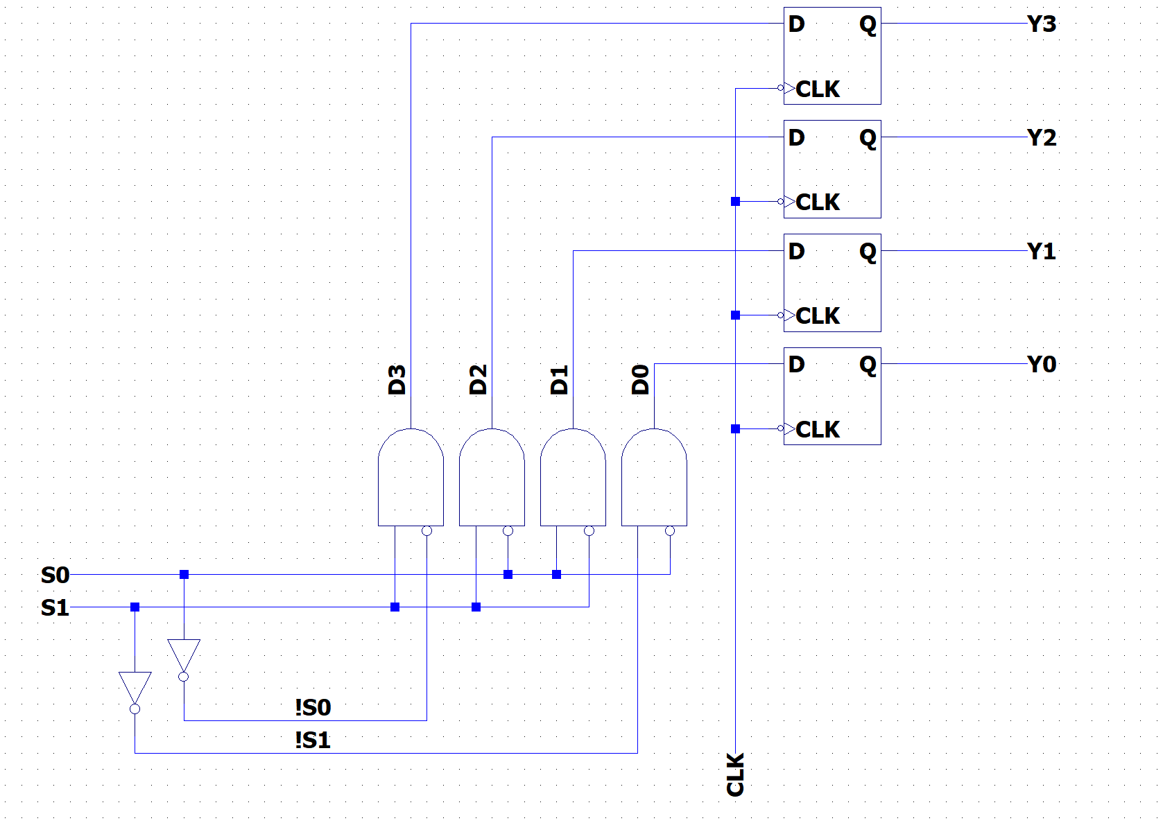
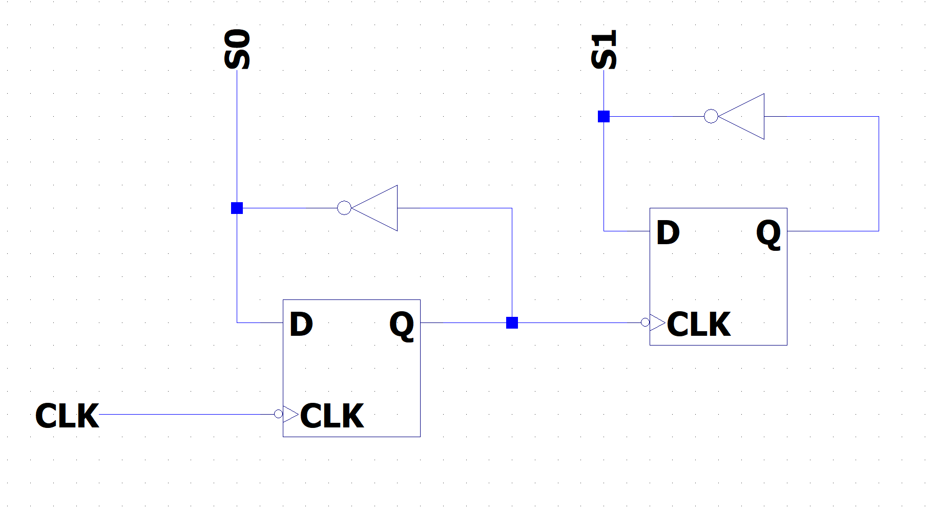
Selector
01/09/2022 at 17:57 • 0 commentsThe “selector” circuit cycles through the different lines of the MUX. It would be very simple to implement this as two astable multivibrators, but over time the signals would likely drift apart. To get around this the selector circuit will be implemented as a frequency divider, seen below. This circuit works because the flip flop only toggle on the falling edge of the clock.
![]()
555 Timer - Timer
We've come full circle. Here's a timer made up of timers...