Jesse Farrell
-
Multiplexer
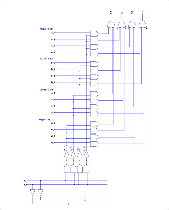
01/09/2022 at 17:54 • 0 commentsThe multiplexer block will route 1 of the 4, 4-bit buses to the drive circuit (the BCD to 7SEG decoder). Its implementation is relatively common and covered in most introductory electronics courses. One difference being I used the basic 1x 555 AND block so there’s a couple extra inverters included.
![]()
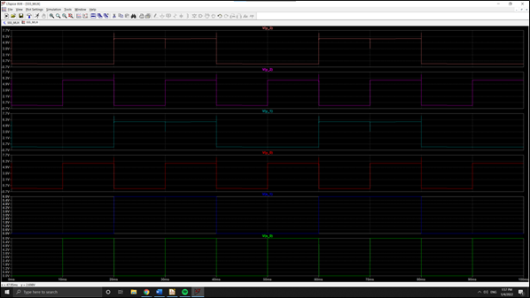
The final 4-1 line MUX requires a total of 26x 555’s, 16 diodes, and a handful of resistors. Its simulation results are shown below. Note that for this simulation channel 0 contains 0000, 1 contains 0101, 2 contains 1010, and 3 contains 1111.
![]()
-
BCD to 7Segment Decoder
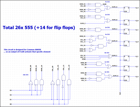
01/09/2022 at 17:51 • 2 commentsThis block takes in 4 bits representing a single digit of the 7-segment display and maps them to a 7-bit output representing digits 0-9. There are two approaches I could take to design this circuit (or atleast two that come to mind). Either I could (a) find the Boolean logic related to each element and create a network of gates that will decode the value on the fly, or I will (b) implement the logic as a MUX. After a bit of tinkering I found that the "Boolean" approach was far more efficient.
Using some Karnough maps, I created the final design can be seen below. Note that I will be using a common anode 7-segment, so to turn on a segment, the output should be 0.
![]()
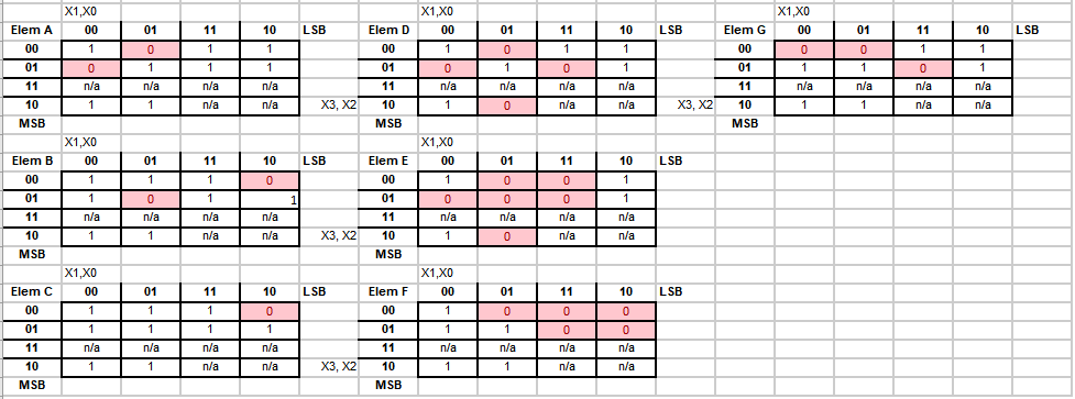
Here are the maps I used for each element. I'm a little rusty on gate simplification so there may be some redundency hidden here.
![]()
NOTE: there was incorrect logic for elelement B, this was discovered during validation (0010) is not a case where B is off
-
D-Type Flip Flop
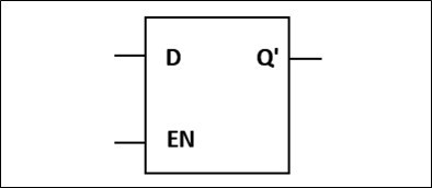
01/09/2022 at 17:34 • 0 commentsDesigning a D type latch (need this for my flip flop) using only 555’s was less trivial than I initially expected. The main issue was implementing the functionality of the enable signal. The latch could easily be brute forced using 5 or so 555’s but this would dramatically bloat the BOM.
The widget will need to store several bytes of data, using excess gates in these latches will dramatically increase the overall cost and footprint of the board. Therefore, some basic active components will be allowed for the D type latch. One good solution posted by Tim was to introduce a pass-through transistor and hold the THRES/TRIG pins at ½ VCC, see below.
![]()
It’s important to note that the implementation above uses the inverted input D. Alternatively, we could think of this as taking in D and outputting Q’ see block below. Obviously, we can remove this inversion with an inverter, but we may be able to avoid this altogether when designing a flip flop. A small capacitor should be added to the emitter of the transistor to help stabilize the SR triggering.
![]()
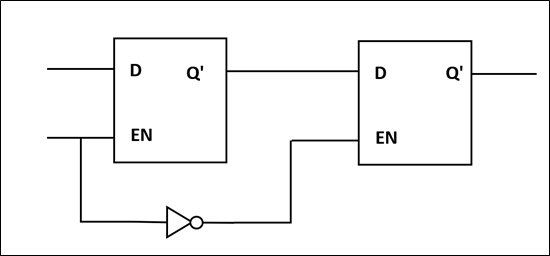
We can now create a flip flop by cascading two of these latches. Note that this flip flop will trigger on the falling edge of the clock signal, and the previously mentioned inversion solves itself.
![]()
*breadboarded this circuit at first but forgot to take captures, they'll be added likely later today (Jan 9th)*
-
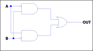
XOR Gate
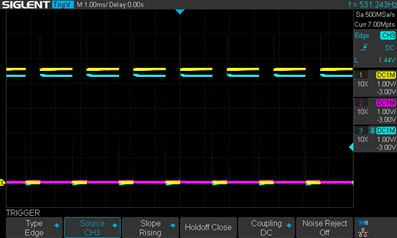
01/09/2022 at 17:28 • 0 commentsAn XOR gate returns a 1 if a single input is high. If all inputs are high, then it returns a 0. The XOR gate may be implemented with 2x 555’s and an OR gate (seen below).
![]()
The breadboarded circuit worked as expected (albeit with the previously mentioned delay). Note there is some voltage drop at the output due to the diode OR circuit.
Yellow = input / Purple = input / Blue = output
![]()
![]()
-
Diode / 555 OR
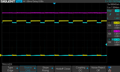
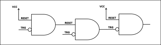
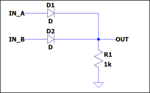
01/09/2022 at 17:24 • 0 commentsAn OR gate takes in two (or more) inputs, and if one or more input is 1, the output will be 1. This would require 3x 555’s as shown below. To keep things uniform, the AND blocks are represented in their single 555 configuration (ie. the TRIG/THRES input is inverting).
![]()
It seems like a waste to do this when we can accomplish the same result with some diodes and a pull-down resistor. However, this gate cannot be cascaded due to the forward voltage of the diodes, doing so may change the logic level of the output. As a precaution the diodes should have low Vf and leakage current.
![]()
One last comment is that we can make a NOR gate using two 555’s as shown below. Both the 555 NOR gate and diode or gate will be used in this design. In general, the 555 OR gate will be avoided to help reduce the overall footprint and cost of this widget.
![]()
-
555 INV
01/09/2022 at 17:12 • 0 commentsBuilding an inverter is simple given we’ve already created an AND gate. If RESET is pulled to VCC the gate will follow the inversion of TRIG/THRES.
![]()
Note that the same ~15us delay was observed when the output transitioned to low.
![]()
-
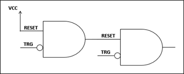
555 AND Gate
01/09/2022 at 02:52 • 0 commentsAn AND gate takes in two (or more) inputs, and outputs a logical 1 when all inputs are 1. All other gates can be expressed with AND gates, so if necessary other gates can be brute forced once this circuit is verified.
Consider the modified schematic shown in below. An AND gate with one inverting input can be constructed using RESET (IN B) and THRES/TRIG (IN A) as the gate inputs.
![]()
THRES/TRIG = 0, RESET = 0, OUT = 0:
Whenever RESET is 0, since the pin is inverting, the SR flip-flop output will be held at 0 in a reset or disabled state.
THRES/TRIG = 1, RESET =0, OUT = 0:
Same reasoning as above; since RESET is 0, the output will be 0.
THRES/TRIG = 0, RESET = 1, OUT = 1:
Now that RESET has been de-asserted, the SR flip-flop will function normally. For the upper comparator the inverting pin will be at a higher potential then the non-inverting pin, so “R” is held low (it won’t be asserted). The lower comparator has the opposite configuration. Its inverting pin will be at a lower potential then its non-inverting, therefore “S” is asserted. Since S is asserted, and RESET is not being held, the flip-flop sets the output to 1.
THRES/TRIG=1, RESET = 1, OUT = 0:
RESET is deserted, so the SR flip-flop won’t be locked low. For the upper comparator the inverting pin will be at a lower potential then the non-inverting pin, so “R” is held high. The lower comparator has the opposite configuration. Its inverting pin will be at a higher potential then its non-inverting, therefore “S” is low. Since S is low and R is high, the flip-flop resets the output to 0.
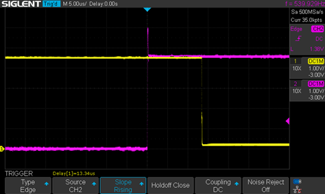
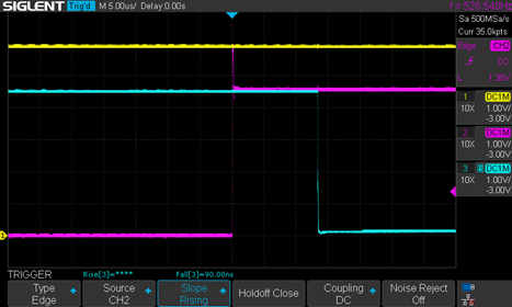
The results of the breadboarded circuit revealed an extended delay of ~15us when disabling the output via the inverting input, see below. Enabling the output via the inverting input of the AND gate took only ~100ns. However, due to the sluggish clock of this widget (~>400Hz or 2500us), the ~15us delay can be ignored.
![]()
-
Block Diagram
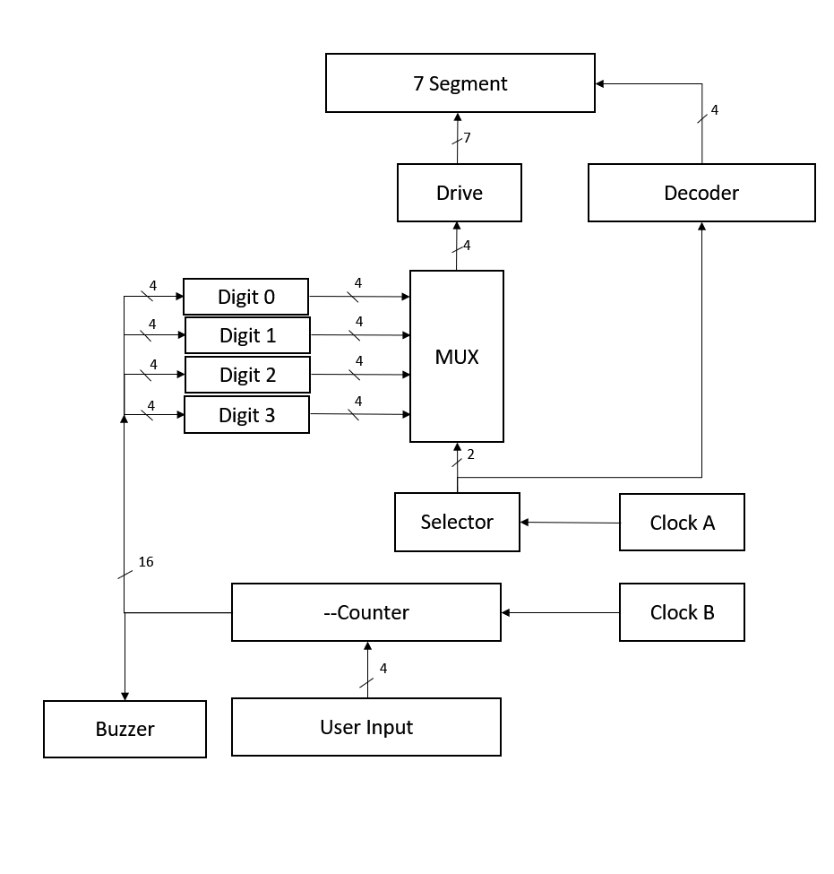
01/09/2022 at 02:47 • 0 commentsKnowing that the 555 can be used for Boolean logic, I developed the bock diagram below. Although I’m sure there are more efficient implementations, I tend to work through the design before looking at any reference designs. This helps me avoid getting bogged down in someone else’s solution and tends to produce more unique results (and more frequent facepalms when I overcomplicate something). Each block must have the following function.
Drive: Input 4 bits representing a single digit of the 7-segment display. The 4-bit input will be mapped to a 7-bit output representing the different elements of a 7-segment digit.
MUX: The multiplexer will route 1 of the 4, 4-bit buses to the drive circuit.
Selector: The “selector” will define the cycling rate for each digit of the display. It could be implemented as a (very exciting) 2-bit counter. The output goes to both the MUX select, and a decoder.
Decoder: This is a basic decoder that takes in a 2-bit input and toggles 1 of 4 bits on the output. The decoder will be used to toggle the common of each digit sequentially.
Clock A: Clock A drives will be greater than ~400Hz and controls the refreshing of the 7-segment display.
Digit #: Stores the 4-bit data, representing a digit 0->9. This block is included as a reference, these digits are incorporated in the flip flops of the counter circuit.
Counter: 16-bit counter (4x 4bits). Counts down in base 10 from 9999 to 0000.
Buzzer: Buzzer circuit that activates when the counter contains all zeros.
Clock B: Clock B drives the countdown timer block at 1 tick per minute.
User Input: The user will be able to toggle each digit by injecting clock pulses into the different blocks of the counter circuit.
![]()
-
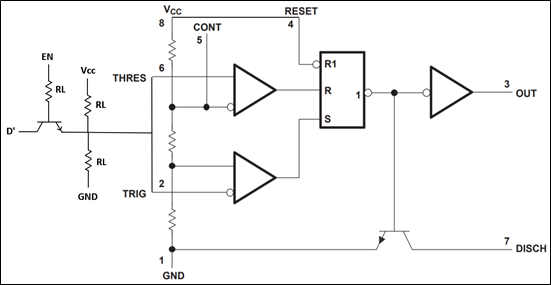
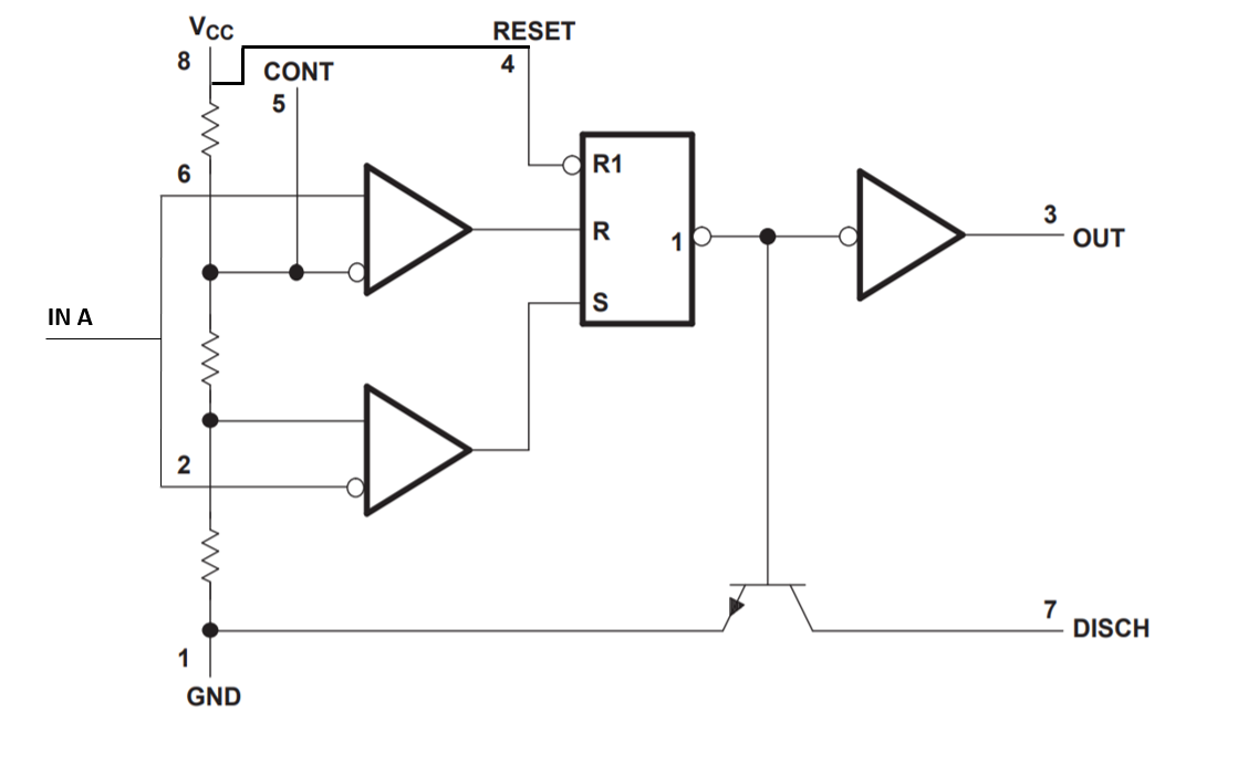
555 IC Overview
01/09/2022 at 02:31 • 0 commentsBefore I can really get into the design, I need to understand the basics of the 555 timer. Although I’ve worked on a handful of projects, I’ve yet to implement one in my designs (hopefully this project will resolve this trend).
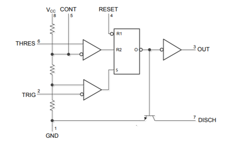
The simplified schematic for the chip is shown below. Internally the 555 primarily contains some comparators, an SR latch, a buffer, and a discharge transistor. That latch will definitely come in handy for gate design down the road.
For specifications, typical output sink/source is about 100mA, and a maximum output near 100kHz. Obviously, these parameters may shift depending on the manufacturer I choose.
![]()
-
Read Me
01/09/2022 at 02:19 • 0 commentsApologies in advance these logs may be sparse. The documentation for the widget is in the project files titled HAS (Hardware Architecture Specification, PDF has a weird visual bug so use DOC version). These logs were added afterword's as a somewhat condensed version of the full document.
555 Timer - Timer
We've come full circle. Here's a timer made up of timers...